

Page 1

SubCompact Board
G E N E - QM7 7 R e v . B
GENE-QM77 Rev.B
Intel® 3rd Generation CoreTM i7-3555LE/
Celeron B847E Processor
10/100/1000Base-TX Ethernet
2 USB3.0, 6 USB 2.0, 4 COM,
8-bit Digital I/O
2 SATA 6.0Gb/s (Optional RAID)
1 CFast™, 1 Mini Card, LPC
GENE-QM77 Manual Rev.B 2nd Ed.
March 17, 2014
Page 2

SubCompact Board
G E N E - QM7 7 R e v . B
Copyright Notice
This document is copyrighted, 2014. All rights are reserved. The
original manufacturer reserves the right to make improvements to
the products described in this manual at any time without notice.
No part of this manual may be reproduced, copied, translated, or
transmitted in any form or by any means without the prior written
permission of the original manufacturer. Information provided in this
manual is intended to be accurate and reliable. However, the
original manufacturer assumes no responsibility for its use, or for
any infringements upon the rights of third parties that may result
from its use.
The material in this document is for product information only and is
subject to change without notice. While reasonable efforts have
been made in the preparation of this document to assure its
accuracy, AAEON assumes no liabilities resulting from errors or
omissions in this document, or from the use of the information
contained herein.
AAEON reserves the right to make changes in the product design
without notice to its users.
i
Page 3

SubCompact Board
G E N E - QM7 7 R e v . B
Acknowledgments
All other products’ name or trademarks are properties of their
respective owners.
AMI is a trademark of American Megatrends Inc.
CFast™ is a trademark of the Compact Flash Association.
Intel® and Core™ are trademarks of Intel® Corporation.
Microsoft Windows® is a registered trademark of Microsoft
Corp.
ITE is a trademark of Integrated Technology Express, Inc.
IBM, PC/AT, PS/2, and VGA are trademarks of International
Business Machines Corporation.
SoundBlaster is a trademark of Creative Labs, Inc.
Please be notified that all other products’ name or trademarks
not be mentioned above are properties of their respective
owners.
ii
Page 4

SubCompact Board
G E N E - QM7 7 R e v . B
Packing List
Before you begin installing your card, please make sure that
the following materials have been shipped:
1 DVD-ROM for Manual (in PDF Format) and
Drivers
1 GENE-QM77 Rev.B with Active Cooler
If any of these items should be missing or damaged, please
contact your distributor or sales representative immediately.
iii
Page 5

SubCompact Board
G E N E - QM7 7 R e v . B
Contents
Chapter 1 General Information
1.1 Introduction ................................................................ 1-2
1.2 Features .................................................................... 1-3
1.3 Specifications ............................................................ 1-4
Chapter 2 Quick Installation Guide
2.1 Safety Precautions .................................................. 2-2
2.2 Location of Connectors and Jumpers ...................... 2-3
2.3 Mechanical Drawing ................................................ 2-5
2.4 List of Jumpers ........................................................ 2-7
2.5 List of Connectors ..................................................... 2-8
2.6 Setting Jumpers ..................................................... 2-10
2.7 LVDS Port 2 Operating VDD Selection (JP2) ......... 2-11
2.8 LVDS Port 1 Backlight Inverter VCC Selection (JP3)
....................................................................................... 2-11
2.9 LVDS Port 2 Backlight Inverter VCC Selection (JP4)
....................................................................................... 2-11
2.10 LVDS Port 1 Operating VDD Selection (JP5) ....... 2-12
2.11 LVDS Port 1 Backlight Lightness Control Mode
Selection (JP6) .............................................................. 2-12
2.12 LVDS Port 2 Backlight Lightness Control Mode
Selection (JP7) .............................................................. 2-12
2.13 COM2 Pin8 Function Selection (JP8) ................... 2-13
2.14 Front Panel Connector (JP9) ................................ 2-13
iv
Page 6

SubCompact Board
G E N E - QM7 7 R e v . B
2.15 Touch Screen 4/5/8-wire Selection (JP10) ........... 2-14
2.16 Clear CMOS (JP11) .............................................. 2-14
2.17 AT/ATX Power Supply Mode Selection (JP12) ..... 2-14
2.18 LVDS Port 1 Inverter/Backlight Connector (CN1) . 2-15
2.19 External +12V Input (CN2) .................................... 2-15
2.20 USB2.0 Port 7 and Port 8 (CN3) ........................... 2-16
2.21 USB2.0 Port 5 and Port 6 (CN4) ........................... 2-16
2.22 USB2.0 Port 3 and Port 4 (CN5) ........................... 2-17
2.23 External +5VSB Input (CN6) ................................. 2-18
2.24 LVDS Port 2 Inverter/Backlight Connector (CN7) . 2-18
2.25 Audio I/O Port Connector (CN8) ........................... 2-19
2.26 LVDS Port 1 Connector (CN9) .............................. 2-19
2.27 LVDS Port 2 Connector (CN10) ............................ 2-21
2.28 COM Port 2 Connector (CN11) ............................. 2-23
2.29 LPT/ Digital I/O Port Connector (CN12) ................ 2-25
2.30 COM Port 3 Connector (CN13) ........................... 2-28
2.31 LPC Port Connector (CN14) ................................. 2-29
2.32 COM Port 4 Connector (CN15) ............................. 2-30
2.33 UIM Card Module (CN16) ..................................... 2-30
2.34 PS/2 Keyboard/Mouse Combo Port Connector (CN17)
....................................................................................... 2-31
2.35 +5VSB Output with SMBus (CN18) ...................... 2-32
2.36 Touch Screen Connector (CN19) .......................... 2-32
2.37 CPU FAN Connector (CN20) ................................ 2-34
2.38 HDMI Connector (CN21) ....................................... 2-36
v
Page 7

SubCompact Board
G E N E - QM7 7 R e v . B
2.39 +5V Output for SATA HDD (CN22) ....................... 2-37
2.40 Realtek LAN (RJ-45) Port (CN23) ......................... 2-37
2.41 Intel LAN (RJ-45) Port (CN24) .............................. 2-38
2.42 USB Port 1 and Port 2 (CN25) .............................. 2-39
2.43 VGA/ DVI Ports (depend on hardware configuration)
(CN26) ........................................................................... 2-40
2.44 COM Port 1 (D-SUB 9) (CN27) ............................. 2-42
2.45 CFast™ Slot (CN28) ............................................. 2-43
2.46 DDR3 SODIMM Slot (CN29) ................................. 2-44
2.47 Mini Card Slot (CN30) ........................................... 2-44
2.48 SATA Port 1 (SATA1)............................................ 2-46
2.49 SATA Port 2 (SATA2)............................................ 2-47
Chapter 3 AMI BIOS Setup
3.1 System Test and Initialization. .................................. 3-2
3.2 AMI BIOS Setup ........................................................ 3-3
Chapter 4 Driver Installation
4.1 Installation……………………………………………..4-3
Appendix A Programming The Watchdog Timer
A.1 Programming ......................................................... A-2
A.2 ITE8728F Watchdog Timer Initial Program ........... A-6
Appendix B I/O Information
B.1 I/O Address Map .................................................... B-2
B.2 Memory Address Map ............................................ B-4
vi
Page 8

SubCompact Board
G E N E - QM7 7 R e v . B
B.3 IRQ Mapping Chart ................................................ B-5
B.4 DMA Channel Assignments.……………………… . B-5
Appendix C Mating Connector
C.1 List of Mating Connectors and Cables.................. C-2
Appendix D RAID & AHCI Settings
D.1 Setting RAID ......................................................... D-2
D.2 Setting AHCI ......................................................... D-9
Appendix E Electrical Specifications for I/O Ports
E.1 Electrical Specifications for I/O Ports ..................... E-2
vii
Page 9

SubCompact Board GENE-QM77 Rev.B
Chapter
1
General
Information
Chapter 1 General Information 1- 1
Page 10

SubCompact Board GENE-QM77 Rev.B
1.1 Introduction
The GENE-QM77 Rev.B supports Intel® Core™ i7-3555LE/
Celeron
®
B847E processor which when paired with the Intel®
QM77/HM76 chipset offers a high performance computing
platform with low power consumption. This new product
supports 204-pin DDR3 SODIMM at speeds of 1333/1600 MHz,
up to 8 GB.
One CFast™ and two SATA 6.0Gb/s (Optional RAID) interfaces
provide ample storages. With dual Gigabit Ethernet, four COM
ports (COM x 3 with HM76), two USB3.0 and six USB2.0, the
GENE-QM77 Rev.B meets the requirements of today’s
demanding applications.
Display requirements are met with an abundance of interfaces
such as CRT, HDMI, and LCD. The graphic engine adopts
®
Intel
QM77/HM76 to offer high definition display function. In
addition, it supports up to two 24-bit Dual-Channel LVDS, and
one optional DVI.
With all of its integrated features, the GENE-QM77 Rev.B
strikes a balance of performance and price. This versatile
product targets Industrial Automation, Entertainment,
KIOSK/POS, Transportation, Banking, and Digital Signage.
Chapter 1 General Information 1-2
Page 11

SubCompact Board GENE-QM77 Rev.B
1.2 Features
Intel® Core™ i7-3555LE/ Celeron® B847E
Processor
Intel
®
QM77/HM76
204-pin DDR3 1333/1600 MHz SODIMM x 1, Up to
8 GB
Gigabit Ethernet x 2
CRT or DVI (optional), 18/24-bit Dual-Channel
LVDS LCD x 2, HDMI x 1
2CH HD Audio
SATA 6.0Gb/s x 2 (Optional RAID), CFast x 1
USB3.0 x 2, USB2.0 x 6, COM x 4 (COM x 3 with
HM76), 8-bit Digital I/O
Mini Card x 1
+12V Only Operation
Supports iAMT with Intel
®
QM77
Onboard 4/5/8-wire Resistive Touch Screen
Controller
Chapter 1 General Information
1-3
Page 12

SubCompact Board GENE-QM77 Rev.B
1.3 Specifications
System
From Factor
Processor
3.5”
®
Intel
Core™i7-3555LE/ Celeron®
B847E Mobile processor
System Memory
Chipset
Ethernet
BIOS
Wake On LAN
Watchdog Timer
H/W Status
Monitoring
Expansion Interface
Trusted Platform
Module
Battery
Power Requirement
Power Consumption
204-pin DDR3 1333/1600 MHz
SODIMM x 1, Max. 8GB
®
Intel
QM77/HM76
®
Intel
82579LM & Realtek
RTL-8111E,
10/100/1000Base-TX, RJ-45 x 2
AMI BIOS-16MB SPI Flash
Yes
Generates a time-out system
reset
Supports power supply voltages
and temperature monitoring
Mini Card x 1, LPC
Infineon SLB 9635TT 1.2
Lithium Battery
+12V, AT/ATX
®
Intel
Core™ i7-3555LE 2.5GHz,
DDR 1333 8G, 2.49A @ +12V
Board Size
Gross Weight
Operating
Temperature
Chapter 1 General Information 1-4
5.75" x 4" (146mm x 101.6mm)
0.88 lb (0.4Kg)
32°F~140°F (0°C~60°C)
Page 13

SubCompact Board GENE-QM77 Rev.B
Storage Temperature
-40°F~176°F (-40°C~80°C)
Operating Humidity
0% ~ 90% relative humidity,
non-condensing
Display: Supports CRT/LCD, HDMI/LCD simultaneous /
iew displays
dual v
Chipset
Memory
®
Intel
QM77/HM76 integrated
Shared system memory up to
512MB
Resolution
Up to 2048x1536 for CRT
Up to 1920 x 1200 for LCD, HDMI,
DVI
HDMI
DVI (Optional)
HDMI x 1
DVI x 1 (optional)
I/O: ITE IT8728F + Fintek F81216D
Storage
Serial Port
SATA 6.0Gb/s x 2 , CFast™ x 1
RS-232 x 3 (QM77)
RS-232 x 2 (HM76)
RS-232/422/485 (auto flow) x 1
Parallel Port
USB
PS/2 Port
Digital I/O
Audio
SPP/EPP/ECP x 1 (by BIOS
setting)
USB3.0 x 2, USB2.0 x 6
Keyboard x 1, Mouse x 1
8-bit Programmable
Line-in, Line-out, Mic-in
Chapter 1 General Information
1-5
Page 14

SubCompact Board
G E N E - Q M 7 7 R e v . B
Chapter
2
Quick
Installation
Guide
Chapter 2 Quick Installation Guide 2-1
Page 15
SubCompact Board
G E N E - Q M 7 7 R e v . B
Always completely disconnect the power cord
from your board whenever you are working on
it. Do not make connections while the power is
on, because a sudden rush of power can
damage sensitive electronic components.
Always ground yourself to remove any static
charge before touching the board. Modern
electronic devices are very sensitive to static
electric charges. Use a grounding wrist strap at
all times. Place all electronic components on a
static-dissipative surface or in a static-shielded
bag when they are not in the chassis
2.1 Safety Precautions
Chapter 2 Quick Installation Guide 2-2
Page 16
SubCompact Board
G E N E - Q M 7 7 R e v . B
Component side
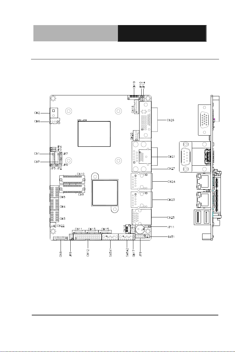
2.2 Location of Connectors and Jumpers
Component Side
Chapter 2 Quick Installation Guide 2-3
Page 17
SubCompact Board
G E N E - Q M 7 7 R e v . B
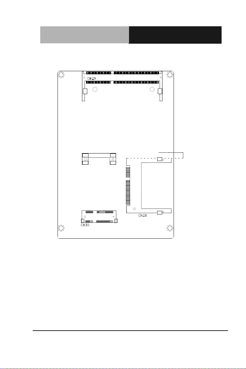
Solder side
Solder Side
Chapter 2 Quick Installation Guide 2-4
Page 18
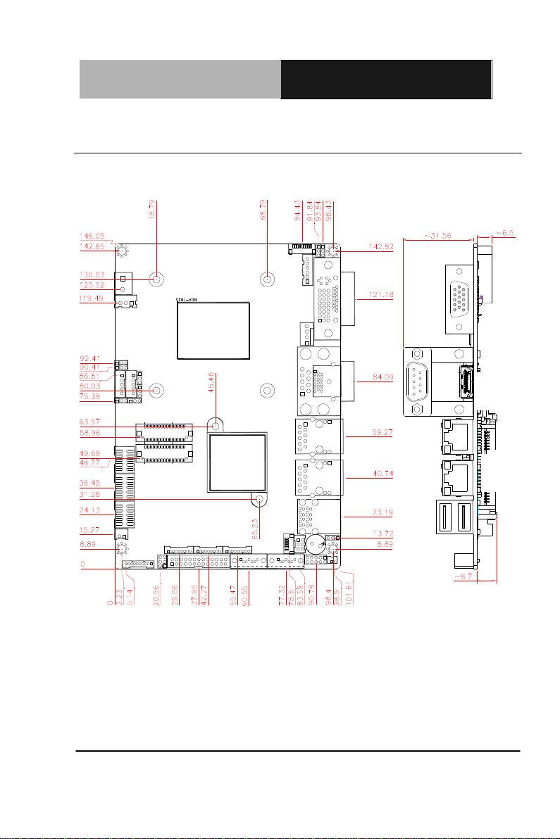
SubCompact Board
G E N E - Q M 7 7 R e v . B
Component side
Solder side
2.3 Mechanical Drawing
Component Side
Chapter 2 Quick Installation Guide 2-5
Page 19
SubCompact Board
G E N E - Q M 7 7 R e v . B
Solder side
Solder Side
Chapter 2 Quick Installation Guide 2-6
Page 20
SubCompact Board
G E N E - Q M 7 7 R e v . B
Label
Function
JP2
LVDS Port 2 Operating VDD Selection
JP3
LVDS Port 1 Backlight Inverter VCC Selection
JP4
LVDS Port 2 Backlight Inverter VCC Selection
JP5
LVDS Port 1 Operating VDD Selection
JP6
LVDS Port 1 Backlight Lightness Control Mode Selection
JP7
LVDS Port 2 Backlight Lightness Control Mode Selection
JP8
COM2 Pin8 Function Selection
JP9
Front Panel Connector
JP10
Touch Screen 4/5/8-wire Mode Selection
JP11
Clear CMOS Jumper
JP12
AT/ATX Power Supply Mode Selection
2.4 List of Jumpers
The board has a number of jumpers that allow you to configure your
system to suit your application.
The table below shows the function of each of the board's jumpers:
Chapter 2 Quick Installation Guide 2-7
Page 21

SubCompact Board
G E N E - Q M 7 7 R e v . B
Label
Function
CN1
LVDS Port 1 Inverter / Backlight Connector
CN2
External +12V Input
CN3
USB 2.0 Ports 7 and 8
CN4
USB 2.0 Ports 5 and 6
CN5
USB 2.0 Ports 3 and 4
CN6
External +5VSB Input
CN7
LVDS Port 2 Inverter / Backlight Connector
CN8
Audio I/O Port
CN9
LVDS Port 1
CN10
LVDS Port 2
CN11
COM Port 2
CN12
LPT / Digital I/O Port
CN13
COM Port 3
CN14
LPC Port
CN15
COM Port 4
CN16
UIM Card Module
CN17
PS/2 Keyboard/Mouse Combo Port
CN18
+5VSB Output w/SMBus
CN19
Touch Screen Connector
2.5 List of Connectors
The board has a number of connectors that allow you to configure your
system to suit your application. The table below shows the function of
each board's connectors:
Chapter 2 Quick Installation Guide 2-8
Page 22

SubCompact Board
G E N E - Q M 7 7 R e v . B
CN20
CPU FAN
CN21
HDMI Connector
CN22
+5V Output for SATA HDD
CN23
Realtek LAN (RJ-45) Port
CN24
Intel LAN (RJ-45) Port
CN25
USB Ports 1 and 2
CN26
VGA / DVI Ports (depend on hardware
configuration)
CN27
COM Port 1 (D-SUB 9) (not available for HM76)
CN28
CFast Slot
CN29
DDR3 SODIMM Slot
CN30
Mini Card Slot
SATA1
SATA Port1 Connector
SATA2
SATA Port 2 Connector
Chapter 2 Quick Installation Guide 2-9
Page 23
SubCompact Board
G E N E - Q M 7 7 R e v . B
1
2
3
Open Closed Closed 2-3
2.6 Setting Jumpers
You configure your card to match the needs of your application by
setting jumpers. A jumper is the simplest kind of electric switch. It
consists of two metal pins and a small metal clip (often protected by a
plastic cover) that slides over the pins to connect them. To “close” a
jumper you connect the pins with the clip.
To “open” a jumper you remove the clip. Sometimes a jumper will have
three pins, labeled 1, 2 and 3. In this case you would connect either
pins 1 and 2 or 2 and 3.
A pair of needle-nose pliers may be helpful when working with jumpers.
If you have any doubts about the best hardware configuration for your
application, contact your local distributor or sales representative before
you make any change.
Generally, you simply need a standard cable to make most
connections.
Chapter 2 Quick Installation Guide 2-10
Page 24
SubCompact Board
G E N E - Q M 7 7 R e v . B
1 2 3
1 2 3
JP2
Function
1-2
+5V
2-3
+3.3V (Default)
1 2 3
1 2 3
JP3
Function
1-2
+12V
2-3
+5V (Default)
1 2 3
1 2 3
JP4
Function
1-2
+12V
2-3
+5V (Default)
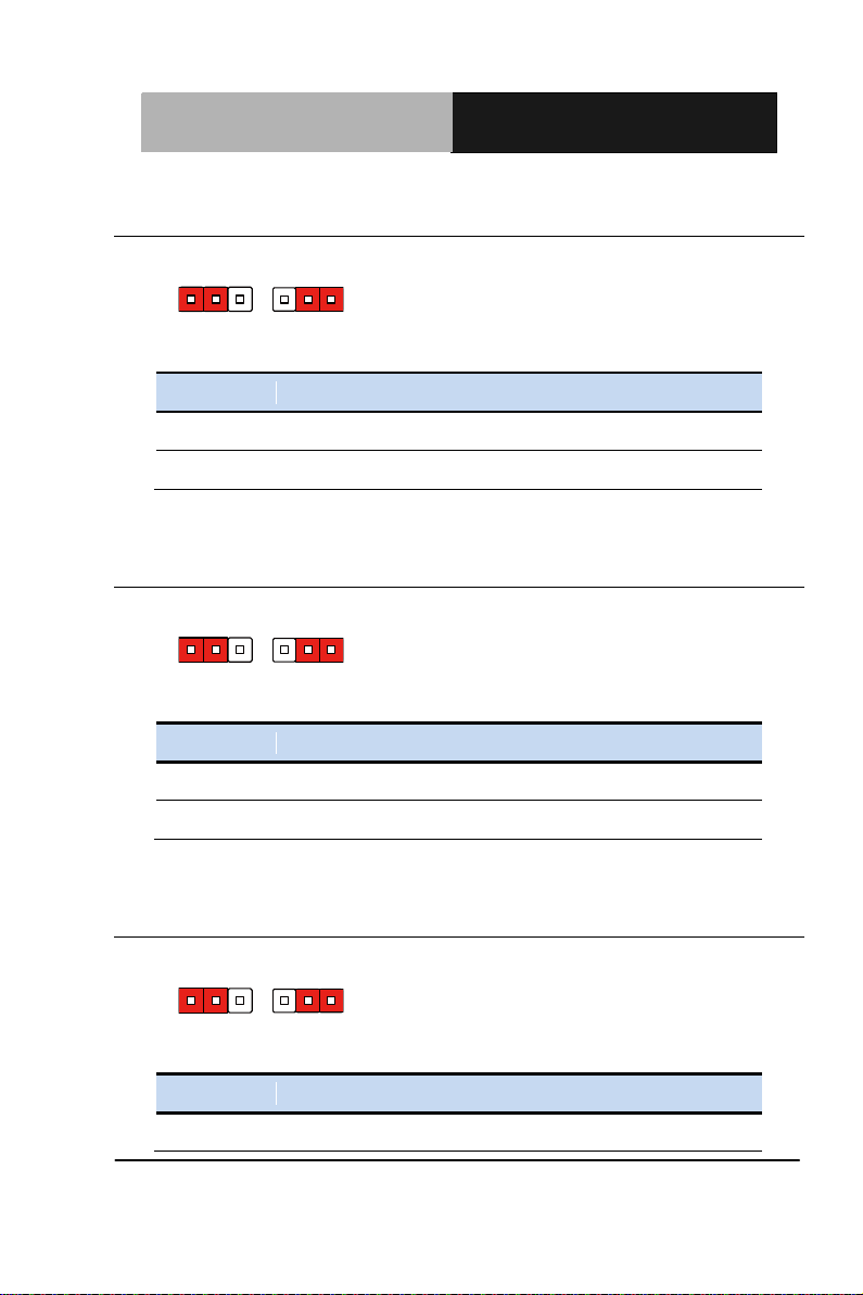
2.7 LVDS Port 2 Operating VDD Selection (JP2)
+5V +3.3V
2.8 LVDS Port 1 Backlight Inverter VCC Selection (JP3)
+12V +5V
2.9 LVDS Port 2 Backlight Inverter VCC Selection (JP4)
+12V +5V
Chapter 2 Quick Installation Guide 2-11
Page 25
SubCompact Board
G E N E - Q M 7 7 R e v . B
1 2 3
1 2 3
JP5
Function
1-2
+5V
2-3
+3.3V (Default)
1 2 3
1 2 3
JP6
Function
1-2
VR Mode (Default)
2-3
PWM Mode
1 2 3
1 2 3
JP7
Function
1-2
VR Mode (Default)
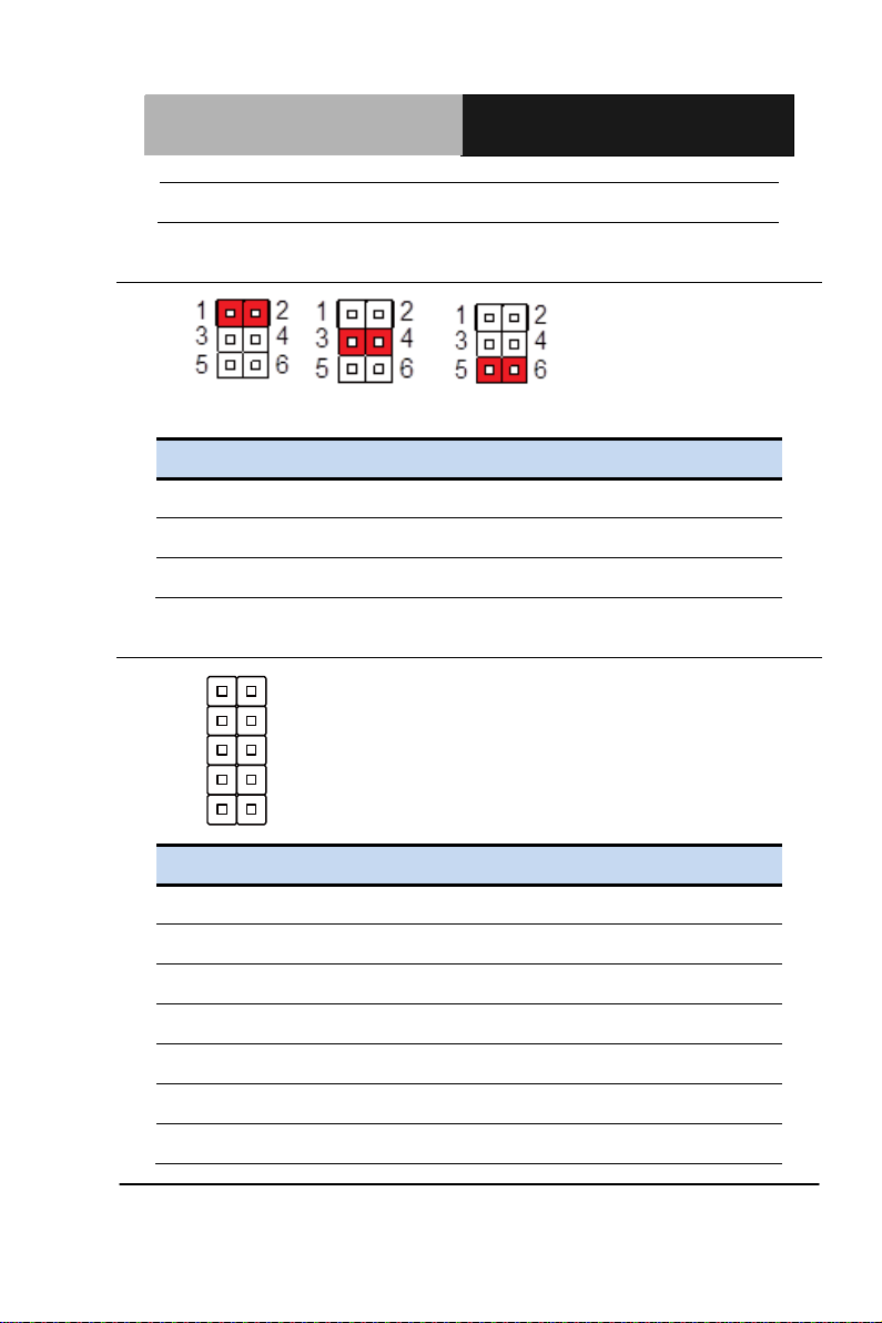
2.10 LVDS Port 1 Operating VDD Selection (JP5)
+5V +3.3V
2.11 LVDS Port 1 Backlight Lightness Control Mode Selection
(JP6)
VR Mode PWM Mode
2.12 LVDS Port 2 Backlight Lightness Control Mode Selection
(JP7)
VR Mode PWM Mode
Chapter 2 Quick Installation Guide 2-12
Page 26
SubCompact Board
G E N E - Q M 7 7 R e v . B
2-3
PWM Mode
JP8
Function
1-2
+12V
3-4
Ring (Default)
5-6
+5V
1
2
3
4
5
6
7
8
9
10
Pin
Signal
1
PWR_BTN-
2
PWR_BTN+
3
HDD_LED-
4
HDD_LED+
5
SPEAKER-
6
SPEAKER+
7
PWR_LED-
2.13 COM2 Pin8 Function Selection (JP8)
+12V Ring +5V
2.14 Front Panel Connector (JP9)
Chapter 2 Quick Installation Guide 2-13
Page 27
SubCompact Board
G E N E - Q M 7 7 R e v . B
8
PWR_LED+
9
H/W RESET-
10
H/W RESET+
1 2 3
1 2 3
JP10
Function
1-2
4/8-wire mode (Default)
2-3
5-wire mode
1 2 3
1 2 3
JP11
Function
1-2
Normal (Default)
2-3
Clear CMOS
1 2 3
1 2 3
JP12
Function
1-2
AT Mode (Default)
2-3
ATX Mode
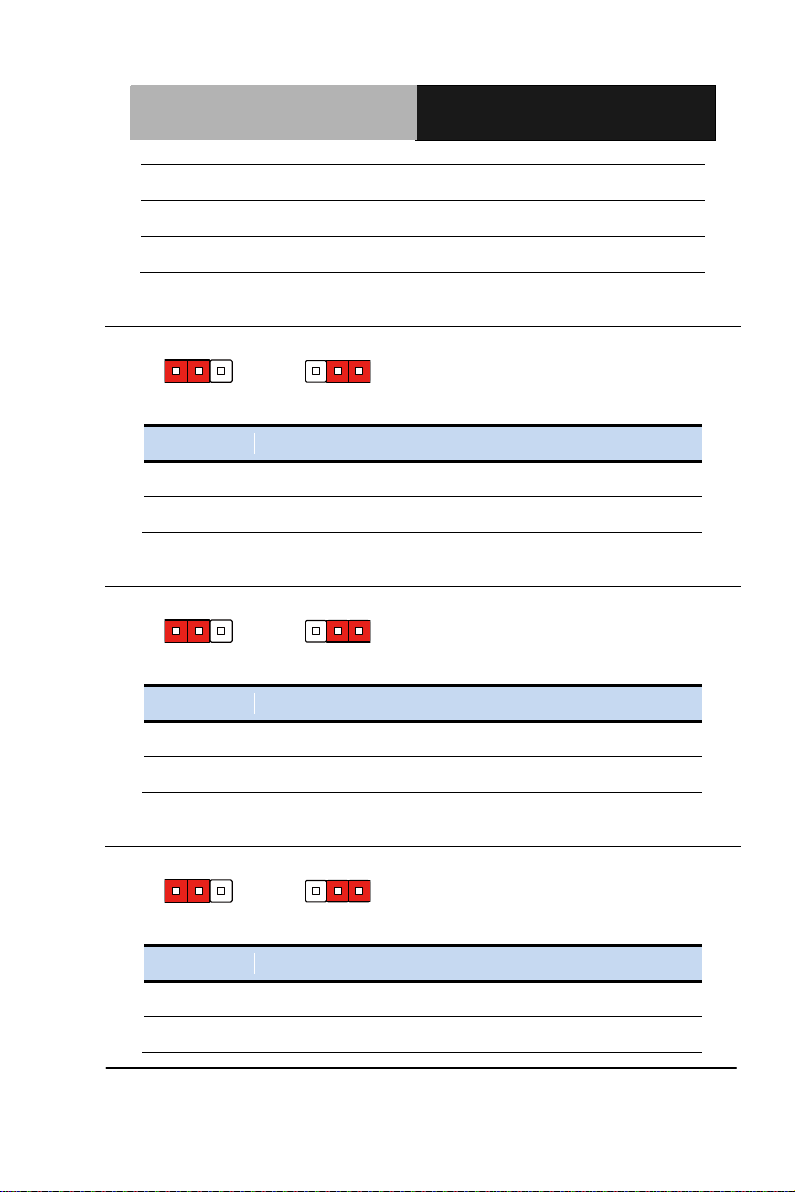
2.15 Touch Screen 4/5/8-Wire Selection (JP10)
4/8-wire mode 5-wire mode
2.16 Clear CMOS (JP11)
Normal Clear CMOS
2.17 AT/ATX Power Supply Mode Selection (JP12)
AT Mode ATX Mode
Chapter 2 Quick Installation Guide 2-14
Page 28
SubCompact Board
G E N E - Q M 7 7 R e v . B
BLK_PWR
2
3
4
5
1
BKL_CONTROL
GND
GND
BKL_ENABLE
Pin
Pin Name
Signal Type
Signal Level
1
BKL_PWR
PWR
+5V / +12V
2
BKL_CONTROL
OUT
3 GND
GND
4 GND
GND
5 BKL_ENABLE
OUT
+5V
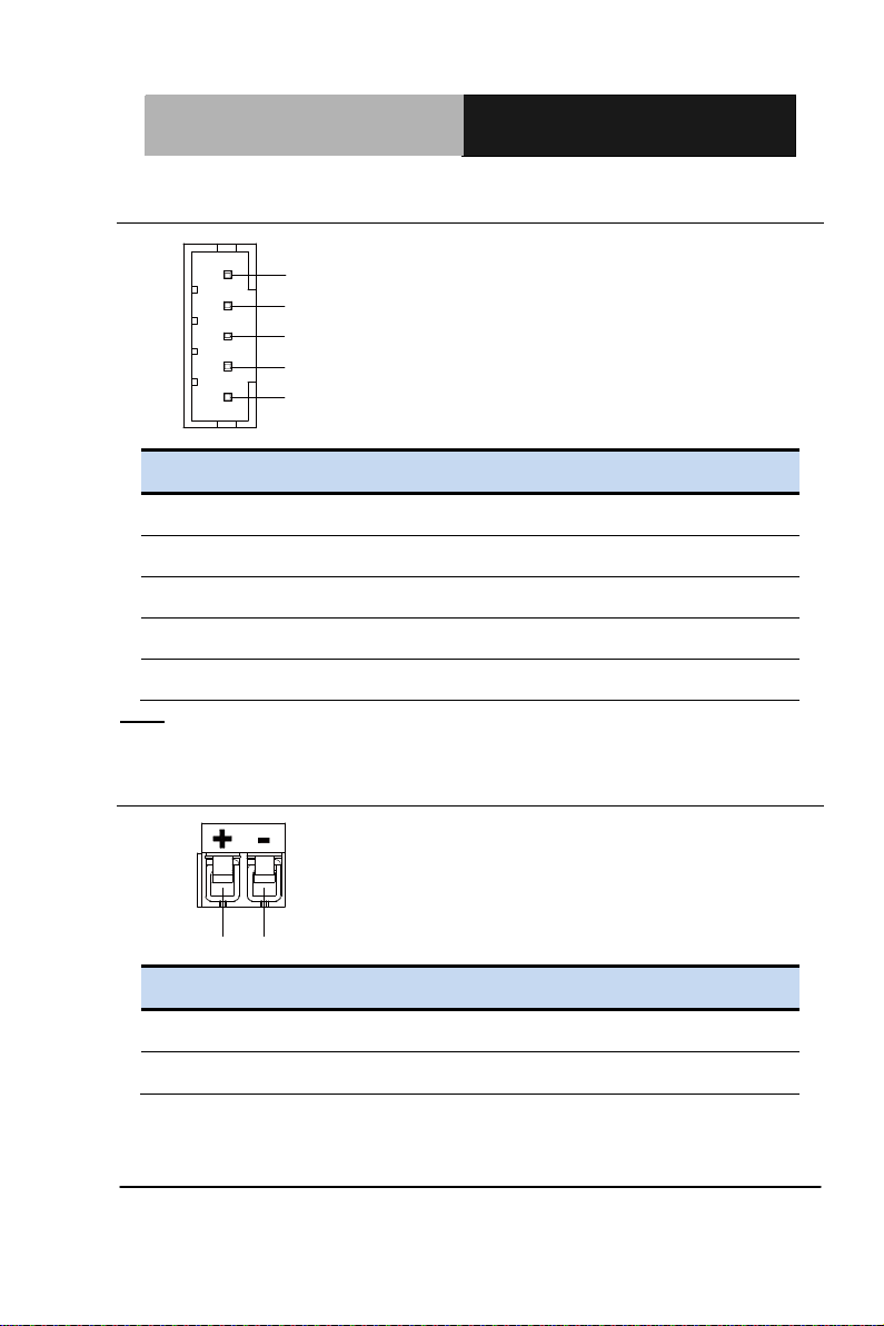
+12V GND
Pin
Pin Name
Signal Type
Signal Level
1
+12V
PWR
+12V
2
GND
GND
2.18 LVDS Port 1 Inverter/ Backlight Connector (CN1)
Note: LVDS1 BKL_PWR can be set to +5V or +12V by JP3.
LVDS1 BKL_CONTROL can be set by JP6.
2.19 External +12V Input (CN2)
Chapter 2 Quick Installation Guide 2-15
Page 29
SubCompact Board
G E N E - Q M 7 7 R e v . B
GND
GND
USB8_D+
USB8_D-
+5VSB
+5VSB
1 2
9 10
USB7_DUSB7_D+
GND
GND
Pin
Pin Name
Signal Type
Signal Level
1
+5VSB
PWR
+5V
2
GND
GND
3 USB7_D-
DIFF
4 GND
GND
5 USB7_D+
DIFF
6 USB8_D+
DIFF
7
GND
GND
8
USB8_D-
DIFF
9
GND
GND
10
+5VSB
PWR
+5V
GND
GND
USB6_D+
USB6_D-
+5VSB
+5VSB
1 2
9 10
USB5_DUSB5_D+
GND
GND
Pin
Pin Name
Signal Type
Signal Level
1
+5VSB
PWR
+5V 2 GND
GND
2.20 USB2.0 Port 7 and Port 8 (CN3)
2.21 USB2.0 Port 5 and Port 6 (CN4)
Chapter 2 Quick Installation Guide 2-16
Page 30
SubCompact Board
G E N E - Q M 7 7 R e v . B
3
USB5_D-
DIFF
4 GND
GND
5 USB5_D+
DIFF
6 USB6_D+
DIFF
7 GND
GND
8 USB6_D-
DIFF
9 GND
GND
10
+5VSB
PWR
+5V
GND
GND
USB4_D+
USB4_D-
+5VSB
+5VSB
1 2
9 10
USB3_DUSB3_D+
GND
GND
Pin
Pin Name
Signal Type
Signal Level
1
+5VSB
PWR
+5V 2 GND
GND
3 USB3_D-
DIFF
4 GND
GND
5
USB3_D+
DIFF
6
USB4_D+
DIFF
7 GND
GND
8
USB4_D-
DIFF
9
GND
GND
2.22 USB2.0 Port 3 and Port 4 (CN5)
Chapter 2 Quick Installation Guide 2-17
Page 31

SubCompact Board
G E N E - Q M 7 7 R e v . B
10
+5VSB
PWR
+5V
+5VSB
GND
PS_ON#
1
2
3
Pin
Pin Name
Signal Type
Signal Level
1
PS_ON#
OUT
+3.3V 2 GND
GND
3 +5VSB
PWR
+5V
BLK_PWR
2
3
4
5
1
BKL_CONTROL
GND
GND
BKL_ENABLE
Pin
Pin Name
Signal Type
Signal Level
1
BKL_PWR
PWR
+5V / +12V
2
BKL_CONTROL
OUT
3 GND
GND
4
GND
GND
5
BKL_ENABLE
OUT
+5V
2.23 External +5VSB Input (CN6)
2.24 LVDS Port 2 Inverter/ Backlight Connector (CN7)
Note: LVDS2 BKL_PWR can be set to +5V or +12V by JP4.
LVDS2 BKL_CTL can be set by JP7.
Chapter 2 Quick Installation Guide 2-18
Page 32

SubCompact Board
G E N E - Q M 7 7 R e v . B
MIC_L1
10
MIC_R
LINE_L_IN
LINE_R_IN
LEFT_OUT
RIGHT_OUT
+5V_AUDIO
GND_AUDIO
GND_AUDIO
GND_AUDIO
Pin
Pin Name
Signal Type
Signal Level
1
MIC_L
IN
2 MIC_R
IN
3 GND_AUDIO
GND
4 LINE_L_IN
IN
5 LINE_R_IN
IN
6 GND_AUDIO
GND
7 LEFT_OUT
OUT
8 GND_AUDIO
GND
9 RIGHT_OUT
OUT
10
+5V_AUDIO
PWR
+5V
2.25 Audio I/O Port Connector (CN8)
Chapter 2 Quick Installation Guide 2-19
Page 33

SubCompact Board
G E N E - Q M 7 7 R e v . B
PIN 1
PIN 2
PIN 30
PIN 29
Pin
Pin Name
Signal Type
Signal Level
1
BKL_ENABLE
OUT
2
BKL_CONTROL
OUT
3 LCD_PWR
PWR
+3.3V/+5V
4
GND
GND
5
LVDS_A_CLK-
DIFF
6
LVDS_A_CLK+
DIFF
7 LCD_PWR
PWR
+3.3V/+5V
8
GND
GND
9 LVDS_DA0-
DIFF
10
LVDS_DA0+
DIFF
11
LVDS_DA1-
DIFF
12
LVDS_DA1+
DIFF
13
LVDS_DA2-
DIFF
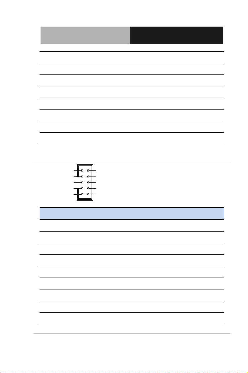
2.26 LVDS Port 1 Connector (CN9)
Chapter 2 Quick Installation Guide 2-20
Page 34

SubCompact Board
G E N E - Q M 7 7 R e v . B
14
LVDS_DA2+
DIFF
15
LVDS_DA3-
DIFF
16
LVDS_DA3+
DIFF
17
DDC_DATA
I/O
+3.3V
18
DDC_CLK
I/O
+3.3V
19
LVDS_DB0-
DIFF
20
LVDS_DB0+
DIFF
21
LVDS_DB1-
DIFF
22
LVDS_DB1+
DIFF
23
LVDS_DB2-
DIFF
24
LVDS_DB2+
DIFF
25
LVDS_DB3-
DIFF
26
LVDS_DB3+
DIFF
27
LCD_PWR
PWR
+3.3V/+5V
28
GND
GND
29
LVDS_B_CLK-
DIFF
30
LVDS_B_CLK+
DIFF
Note: LVDS1 LCD_PWR can be set to +3.3V or +5V by JP5.
Chapter 2 Quick Installation Guide 2-21
Page 35

SubCompact Board
G E N E - Q M 7 7 R e v . B
PIN 1
PIN 2
PIN 30
PIN 29
Pin
Pin Name
Signal Type
Signal Level
1
BKL_ENABLE
OUT
2
BKL_CONTROL
OUT
3
LCD_PWR
PWR
+3.3V/+5V
4
GND
GND
5 LVDS_A_CLK-
DIFF
6 LVDS_A_CLK+
DIFF
7
LCD_PWR
PWR
+3.3V/+5V
8
GND
GND
9 LVDS_DA0-
DIFF
10
LVDS_DA0+
DIFF
11
LVDS_DA1-
DIFF
12
LVDS_DA1+
DIFF
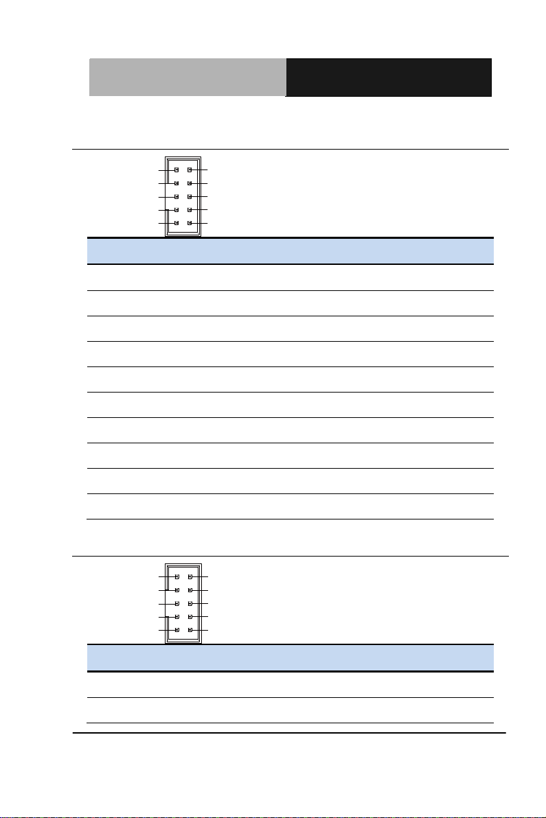
2.27 LVDS Port 2 Connector (CN10)
Chapter 2 Quick Installation Guide 2-22
Page 36

SubCompact Board
G E N E - Q M 7 7 R e v . B
13
LVDS_DA2-
DIFF
14
LVDS_DA2+
DIFF
15
LVDS_DA3-
DIFF
16
LVDS_DA3+
DIFF
17
DDC_DATA
I/O
+3.3V
18
DDC_CLK
I/O
+3.3V
19
LVDS_DB0-
DIFF
20
LVDS_DB0+
DIFF
21
LVDS_DB1-
DIFF
22
LVDS_DB1+
DIFF
23
LVDS_DB2-
DIFF
24
LVDS_DB2+
DIFF
25
LVDS_DB3-
DIFF
26
LVDS_DB3+
DIFF
27
LCD_PWR
PWR
+3.3V/+5V
28
GND
GND
29
LVDS_B_CLK-
DIFF
30
LVDS_B_CLK+
DIFF
Note: LVDS2 LCD_PWR can be set to +3.3V or +5V by JP2.
Chapter 2 Quick Installation Guide 2-23
Page 37

SubCompact Board
G E N E - Q M 7 7 R e v . B
1
2
3
4
5
6
7
8
9
Pin
Pin Name
Signal Type
Signal Level
1
DCD
IN
2 DSR
IN
3 RX
IN
4 RTS
OUT
±9V 5 TX
OUT
±9V 6 CTS
IN
7 DTR
OUT
±9V
8
RI/+5V/+12V
IN/ PWR
+5V/+12V 9 GND
GND
Pin
Pin Name
Signal Type
Signal Level
1
RS422_TX-
OUT
±5V
2
NC
2.28 COM Port 2 Connector (CN11)
RS-232
RS-422
Chapter 2 Quick Installation Guide 2-24
Page 38

SubCompact Board
G E N E - Q M 7 7 R e v . B
3
RS422_RX+
IN
4 NC
5 RS422_TX+
OUT
±5V 6 NC
7 RS422_RX-
IN
8 NC/+5V/+12V
PWR
+5V/+12V 9 GND
GND
Pin
Pin Name
Signal Type
Signal Level
1
RS485_D-
I/O
±5V 2 NC
3 NC
4 NC
5
RS485_D+
I/O
±5V
6
NC
7 NC
8 NC/+5V/+12V
PWR
+5V/+12V 9 GND
GND
RS-485
Note: COM2 RS-232/422/485 can be set by BIOS setting. Default is RS-232.
Pin 8 function can be set by JP8.
Chapter 2 Quick Installation Guide 2-25
Page 39

SubCompact Board
G E N E - Q M 7 7 R e v . B
N.C
N.C
N.C
N.C
N.C
GND
GND
GND
GND
GND
GND
GND
GND
N.C
DIO0
DIO1
DIO2
DIO3
N.C
N.C
N.C
N.C
DIO7
DIO6
DIO5
DIO4
STROBE#
1 2
25 26
1 2
25 26
AFD#
ERROR#
PRINT#
SLIN#
GND
GND
GND
GND
GND
GND
GND
GND
N.C
PD0
PD1
PD2
PD3
PD4
PD5
PD6
PD7
ACK#
BUSY
PE
SLCT
LPT Mode DIO Mode
Pin
Pin Name
Signal Type
Signal Level
1
STROBE#
IN
2 AFD#
I/O
3 PD0
I/O
4 ERROR#
IN
5 PD1
I/O
6 PRINT#
I/O
7 PD2
I/O
8 SLIN#
I/O
9 PD3
I/O
10
GND
GND
11
PD4
I/O
12
GND
GND
13
PD5
I/O
2.29 LPT/ Digital I/O Port Connector (CN12)
LPT Mode
Chapter 2 Quick Installation Guide 2-26
Page 40

SubCompact Board
G E N E - Q M 7 7 R e v . B
14
GND
GND
15
PD6
I/O
16
GND
GND
17
PD7
I/O
18
GND
GND
19
ACK#
IN
20
GND
GND
21
BUSY
IN
22
GND
GND
23
PE
IN
24
GND
GND
25
SLCT
IN
26
NC
N.C
N.C
N.C
N.C
N.C
GND
GND
GND
GND
GND
GND
GND
GND
N.C
DIO0
DIO1
DIO2
DIO3
N.C
N.C
N.C
N.C
DIO7
DIO6
DIO5
DIO4
1 2
25 26
Note: LPT / Digital IO can be set by BIOS setting. Default is LPT Function
DIO Mode
Chapter 2 Quick Installation Guide 2-27
Page 41

SubCompact Board
G E N E - Q M 7 7 R e v . B
Pin
Pin Name
Signal Type
Signal Level
1
NC
2 NC
3 DIO0
I/O
+5V 4 NC
5 DIO1
I/O
+5V 6 NC
7 DIO2
I/O
+5V 8 NC
9 DIO3
I/O
+5V
10
GND
GND
11
NC
12
GND
GND
13
NC
14
GND
GND
15
NC
16
GND
GND
17
NC
18
GND
GND
19
DIO7
I/O
+5V
20
GND
GND
21
DIO6
I/O
+5V
22
GND
GND
23
DIO5
I/O
+5V
Chapter 2 Quick Installation Guide 2-28
Page 42

SubCompact Board
G E N E - Q M 7 7 R e v . B
24
GND
GND
25
DIO4
I/O
+5V
26
NC
GPIO Port # /
Pin Name
Location
(Pin #)
I/O Port
Access Address
Port 1/DIO0
3
Bit 0 of 0xA06
Port 2/DIO1
5
Bit 1 of 0xA06
Port 3/DIO2
7
Bit 2 of 0xA06
Port 4/DIO3
9
Bit 3 of 0xA06
Port 5/DIO4
25
Bit 0 of 0xA07
Port 6/DIO5
23
Bit 1 of 0xA07
Port 7/DIO6
21
Bit 2 of 0xA07
Port 8/DIO7
19
Bit 3 of 0xA07
Pin
Pin Name
Signal Type
Signal Level
1
DCD
IN
2
DSR
IN
3 RX
IN
4
RTS
OUT
±9V
5
TX
OUT
±9V
DCD
DSR
RX
RTS
TX
CTS
DTR
RI
GND
2.30 COM Port 3 Connector (CN13)
Chapter 2 Quick Installation Guide 2-29
Page 43

SubCompact Board
G E N E - Q M 7 7 R e v . B
LAD0 1
12
LAD1
LAD2
LAD3
LFRAME#
LRESET#
LDRQ0
LDRQ1
SERIRQ
GND
LCLK
+3.3V
6
CTS
IN
7 DTR
OUT
±9V 8 RI
IN
9 GND
GND
Pin
Pin Name
Signal Type
Signal Level
1
LAD0
I/O
+3.3V 2 LAD1
I/O
+3.3V 3 LAD2
I/O
+3.3V 4 LAD3
I/O
+3.3V 5 +3.3V
PWR
+3.3V
6
LFRAME#
IN
7
LRESET#
OUT
+3.3V
8
GND
GND
9
LCLK
OUT
10
LDRQ0
IN
11
LDRQ1
IN
2.31 LPC Port Connector (CN14)
Chapter 2 Quick Installation Guide 2-30
Page 44

SubCompact Board
G E N E - Q M 7 7 R e v . B
12
SERIRQ
I/O
+3.3V
Pin
Pin Name
Signal Type
Signal Level
1
DCD
IN
2 DSR
IN
3 RX
IN
4 RTS
OUT
±9V 5 TX
OUT
±9V 6 CTS
IN
7 DTR
OUT
±9V 8 RI
IN
9 GND
GND
UIM_PWR 1
6
UIM_RST
UIM_CLK
GND
UIM_VPP
UIM_DATA
DCD
DSR
RX
RTS
TX
CTS
DTR
RI
GND
2.32 COM Port 4 Connector (CN15)
2.33 UIM Card Module (CN16)
Chapter 2 Quick Installation Guide 2-31
Page 45

SubCompact Board
G E N E - Q M 7 7 R e v . B
Pin
Pin Name
Signal Type
Signal Level
1
UIM_PWR
PWR
2 UIM_RST
IN
3 UIM_CLK
IN
4 GND
GND
5 UIM_VPP
PWR
6 UIM_DATA
I/O
KB_CLK
KB_DATA
1
5 6
2
MS_DATA
+5VSBGND
MS_CLK
Pin
Pin Name
Signal Type
Signal Level
1
KB_DATA
I/O
+5V
2
KB_CLK
I/O
+5V 3 GND
GND
4 +5VSB
PWR
+5V 5 MS_DATA
I/O
+5V 6 MS_CLK
I/O
+5V
2.34 PS/2 Keyboard/Mouse Combo Port Connector (CN17)
Chapter 2 Quick Installation Guide 2-32
Page 46

SubCompact Board
G E N E - Q M 7 7 R e v . B
SMB_DATA
1
6
GND
SMB_CLK
GND
PS_ON#
+5VSB
GND
1
9
1
9
1
9
TOP EXCITE
BOTTOM EXCITE
LEFT EXCITE
RIGHT EXCITE
TOP SENSE
BOTTOM SENSE
LEFT SENSE
RIGHT SENSE
GND
TOP
BOTTOM
LEFT
RIGHT
NC
NC
NC
NC
GND
UL(Y)
UR(H)
LL(L)
LR(X)
SENSE(S)
NC
NC
NC
8 Wires 4 Wires 5 Wires
Pin
Pin Name
Signal Type
Signal Level
1
SMB_DATA
I/O
+3.3V 2 GND
GND
3 SMB_CLK
I/O
+3.3V 4 GND
GND
5 PS_ON#
OUT
+3.3V
6
+5VSB
PWR
+5V
Pin
Pin Name
Signal Type
Signal Level
1
GND
GND
2 TOP EXCITE
IN
3
BOTTOM EXCITE
IN
2.35 +5VSB Output w/SMBus (CN18)
2.36 Touch Screen Connector (CN19)
8-wire
Chapter 2 Quick Installation Guide 2-33
Page 47

SubCompact Board
G E N E - Q M 7 7 R e v . B
1
9
1
9
GND
TOP
BOTTOM
LEFT
RIGHT
NC
NC
NC
NC
GND
UL(Y)
UR(H)
LL(L)
LR(X)
SENSE(S)
NC
NC
NC
4
LEFT EXCITE
IN
5
RIGHT EXCITE
IN
6 TOP SENSE
IN
7
BOTTOM SENSE
IN
8 LEFT SENSE
IN
9 RIGHT SENSE
IN
Pin
Pin Name
Signal Type
Signal Level
1
GND
GND
2 TOP
IN
3 BOTTOM
IN
4
LEFT
IN
5
RIGHT
IN
6 NC
7 NC
8 NC
9
NC
4-wire
Chapter 2 Quick Installation Guide 2-34
Page 48

SubCompact Board
G E N E - Q M 7 7 R e v . B
1
9
GND
UL(Y)
UR(H)
LL(L)
LR(X)
SENSE(S)
NC
NC
NC
Pin
Pin Name
Signal Type
Signal Level
1
GND
GND
2 UL(Y)
IN
3 UR(H)
IN
4 LL(L)
IN
5
LR(X)
IN
6
SENSE(S)
IN
7 NC
8 NC
9 NC
GND
123
FAN_POWER
FAN_TAC
5-wire
Note: Touch mode can be set by JP10
2.37 CPU FAN Connector (CN20)
Chapter 2 Quick Installation Guide 2-35
Page 49

SubCompact Board
G E N E - Q M 7 7 R e v . B
Pin
Pin Name
Signal Type
Signal Level
1
GND
GND
2 FAN_POWER
PWR
+5V 3 FAN_TAC
IN
1
218
19
Pin
Pin Name
Signal Type
Signal Level
1
TMDS_DAT2+
DIFF
2 GND
GND
3 TMDS_DAT2-
DIFF
4
TMDS_DAT1+
DIFF
5
GND
GND
6 TMDS_DAT1-
DIFF
7 TMDS_DAT0+
DIFF
8 GND
GND
9 TMDS_DAT0-
DIFF
10
TMDS_CLK+
DIFF
11
GND
GND
12
TMDS_CLK-
DIFF
13
NC
14
NC
2.38 HDMI Connector (CN21)
Chapter 2 Quick Installation Guide 2-36
Page 50

SubCompact Board
G E N E - Q M 7 7 R e v . B
15
DDC_CLK
I/O
+5V
16
DDC_DATA
I/O
+5V
17
GND
GND
18
+5V
I/O
+5V
19
HPLG_DETECT
IN
+5V
GND
Pin
Pin Name
Signal Type
Signal Level
1
+5V
PWR
+5V 2 GND
GND
1
ACT/LINK
LED
SPEED
LED
8
Pin
Pin Name
Signal Type
Signal Level
1
MDI0+
DIFF
2
MDI0-
DIFF
3 MDI1+
DIFF
4 MDI2+
DIFF
2.39 +5V Output for SATA HDD (CN22)
2.40 Realtek LAN (RJ-45) Port (CN23)
Chapter 2 Quick Installation Guide 2-37
Page 51

SubCompact Board
G E N E - Q M 7 7 R e v . B
5
MDI2-
DIFF
6 MDI1-
DIFF
7 MDI3+
DIFF
8 MDI3-
DIFF
1
ACT/LINK
LED
SPEED
LED
8
Pin
Pin Name
Signal Type
Signal Level
1
MDI0+
DIFF
2
MDI0-
DIFF
3
MDI1+
DIFF
4 MDI2+
DIFF
5 MDI2-
DIFF
6 MDI1-
DIFF
7 MDI3+
DIFF
8
MDI3-
DIFF
2.41 Intel LAN (RJ-45) Port (CN24)
Chapter 2 Quick Installation Guide 2-38
Page 52

SubCompact Board
G E N E - Q M 7 7 R e v . B
10
Port 2
Port 1
11 12 13
1 2 3 4
1415161718
5
6
7
89
Pin
Pin Name
Signal Type
Signal Level
1
+5VSB
PWR
+5V
2
USB1_D-
DIFF
3 USB1_D+
DIFF
4 GND
GND
5 USB1_SSRX−
DIFF
6 USB1_SSRX+
DIFF
7
GND
GND
8
USB1_SSTX−
DIFF
9 USB1_SSTX+
DIFF
10
+5VSB
PWR
+5V
11
USB2_D-
DIFF
12
USB2_D+
DIFF
13
GND
GND
14
USB2_SSRX−
DIFF
15
USB2_SSRX+
DIFF
2.42 USB Port 1 and Port 2 (CN25)
Chapter 2 Quick Installation Guide 2-39
Page 53

SubCompact Board
G E N E - Q M 7 7 R e v . B
16
GND
GND
17
USB2_SSTX−
DIFF
18
USB2_SSTX+
DIFF
1
1
9
C1C5C2
C3 C4
17
8
16
24
610
1115
5
Pin
Pin Name
Signal Type
Signal Level
1
RED
OUT
2
GREEN
OUT
3
BLUE
OUT
4 NC
5 GND
GND
6
RED_GND_RTN
GND
7
GREEN_GND_RTN
GND
8
BLUE_GND_RTN
GND
9
+5V
PWR
+5V
10
GND
GND
11
NC
2.43 VGA / DVI Ports (depend on hardware configuration) (CN26)
VGA
Chapter 2 Quick Installation Guide 2-40
Page 54

SubCompact Board
G E N E - Q M 7 7 R e v . B
12
DDC_DATA
I/O
+5V
13
HSYNC
OUT
14
VSYNC
OUT
15
DDC_CLK
I/O
+5V
Pin
Pin Name
Signal Type
Signal Level
1
TMDS_DAT2+
DIFF
2
TMDS_DAT2-
DIFF
3 GND
GND
4 NC
I/O
5 NC
I/O
6 DDC_CLK
I/O
+5V
7
DDC_DATA
I/O
+5V
8
VSYNC
OUT
9 TMDS_DAT1-
DIFF
10
TMDS_DAT1+
DIFF
11
GND
GND
12
TMDS_DAT3-
DIFF
13
TMDS_DAT3+
DIFF
14
+5V
PWR
+5V
15
GND
GND
16
HPLG_DETECT
IN
17
TMDS_DAT0-
DIFF
DVI
Chapter 2 Quick Installation Guide 2-41
Page 55

SubCompact Board
G E N E - Q M 7 7 R e v . B
18
TMDS_DAT0+
DIFF
19
GND
GND
20
NC
21
NC
22
GND
GND
23
TMDS_CLK+
DIFF
24
TMDS_CLK-
DIFF
C1
RED
OUT
C2
GREEN
OUT
C3
BLUE
OUT
C4
HSYNC
OUT
C5
GND_ANALOG
GND
1 5
6 9
Pin
Pin Name
Signal Type
Signal Level
1
DCD
IN
2 RX
IN
3
TX
OUT
±9V
4
DTR
OUT
±9V
5
GND
GND
6
DSR
IN
2.44 COM Port 1 (D-SUB 9) (CN27) (not available for HM76)
Chapter 2 Quick Installation Guide 2-42
Page 56

SubCompact Board
G E N E - Q M 7 7 R e v . B
7
RTS
OUT
±9V 8 CTS
IN
9 RI
IN
Pin
Pin Name
Signal Type
Signal Level
S1
GND
GND
S2
SATA_TX+
DIFF
S3
SATA_TX-
DIFF
S4
GND
GND
S5
SATA_RX-
DIFF
S6
SATA_RX+
DIFF
S7
GND
GND
PC1
NC
PC2
GND
GND
PC3
NC
PC4
NC
PC5
NC
PC6
NC
PC7
GND
GND
PC8
NC
PC9
NC
PC10
NC
PC11
NC
2.45 CFast Slot (CN28)
Chapter 2 Quick Installation Guide 2-43
Page 57

SubCompact Board
G E N E - Q M 7 7 R e v . B
PC12
NC
PC13
+3.3V
PWR
+3.3V
PC14
+3.3V
PWR
+3.3V
PC15
GND
GND
PC16
GND
GND
PC17
NC
Pin
Pin Name
Signal Type
Signal Level
1
PCIE_WAKE#
IN
2 +3.3VSB
PWR
+3.3V 3 NC
4 GND
GND
5 NC
6 +1.5V
PWR
+1.5V
7
PCIE_CLK_REQ#
IN
8 UIM_PWR
PWR
9 GND
GND
10
UIM_DATA
I/O
11
PCIE_REF_CLK-
DIFF
12
UIM_CLK
IN
2.46 DDR3 SODIMM Slot (CN29)
Standard specification
2.47 Mini Card Slot (CN30)
Chapter 2 Quick Installation Guide 2-44
Page 58

SubCompact Board
G E N E - Q M 7 7 R e v . B
13
PCIE_REF_CLK+
DIFF
14
UIM_RST
IN
15
GND
GND
16
UIM_VPP
PWR
17
NC
18
GND
GND
19
NC
20
W_DISABLE#
OUT
+3.3V
21
GND
GND
22
PCIE_RST#
OUT
+3.3V
23
PCIE_RX-
DIFF
24
+3.3VSB
PWR
+3.3V
25
PCIE_RX+
DIFF
26
GND
GND
27
GND
GND
28
+1.5V
PWR
+1.5V
29
GND
GND
30
SMB_CLK
I/O
+3.3V
31
PCIE_TX-
DIFF
32
SMB_DATA
I/O
+3.3V
33
PCIE_TX+
DIFF
34
GND
GND
35
GND
GND
36
USB_D-
DIFF
Chapter 2 Quick Installation Guide 2-45
Page 59

SubCompact Board
G E N E - Q M 7 7 R e v . B
37
GND
GND
38
USB_D+
DIFF
39
+3.3VSB
PWR
+3.3V
40
GND
GND
41
+3.3VSB
PWR
+3.3V
42
NC
43
GND
GND
44
NC
45
NC
46
NC
47
NC
48
+1.5V
PWR
+1.5V
49
NC
50
GND
GND
51
NC
52
+3.3VSB
PWR
+3.3V
Pin 1 Pin 7
Pin
Pin Name
Signal Type
Signal Level
1
GND
GND
2
SATA_TX+
DIFF
2.48 SATA Port 1 (SATA1)
Chapter 2 Quick Installation Guide 2-46
Page 60

SubCompact Board
G E N E - Q M 7 7 R e v . B
3
SATA_TX-
DIFF
4 GND
GND
5 SATA_RX-
DIFF
6 SATA_RX+
DIFF
7 GND
GND
Pin 1 Pin 7
Pin
Pin Name
Signal Type
Signal Level
1
GND
GND
2 SATA_TX+
DIFF
3 SATA_TX-
DIFF
4
GND
GND
5
SATA_RX-
DIFF
6 SATA_RX+
DIFF
7 GND
GND
2.48 SATA Port 2 (SATA2)
Chapter 2 Quick Installation Guide 2-47
Page 61

SubCompact Board
G E N E - Q M 7 7 R e v . B
部件名称
有毒有害物质或元素
铅
(Pb)
汞
(Hg) 镉 (Cd)
六价铬
(Cr(VI))
多溴联苯
(PBB)
多溴二苯醚
(PBDE)
印刷电路板
及其电子组件
× ○ ○ ○ ○
○
外部信号
连接器及线材
× ○ ○ ○ ○
○
O:表示该有毒有害物质在该部件所有均质材料中的含量均在
SJ/T 11363-2006 标准规定的限量要求以下。
X:表示该有毒有害物质至少在该部件的某一均质材料中的含量超出
SJ/T 11363-2006 标准规定的限量要求。
备注:此产品所标示之环保使用期限,系指在一般正常使用状况下。
Below Table for China RoHS Requirements
产品中有毒有害物质或元素名称及含量
AAEON Main Board/ Daughter Board/ Backplane
Chapter 2 Quick Installation Guide 2-48
Page 62

SubCompact Board GENE-QM77 Rev.B
Chapter
3
AMI
BIOS Setup
Chapter 3 AMI BIOS Setup 3-1
Page 63

SubCompact Board GENE-QM77 Rev.B
3.1 System Test and Initialization
These routines test and initialize board hardware. If the routines
encounter an error during the tests, you will either hear a few short
beeps or see an error message on the screen. There are two kinds
of errors: fatal and non-fatal. The system can usually continue the
boot up sequence with non-fatal errors.
System configuration verification
These routines check the current system configuration against the
values stored in the CMOS memory. If they do not match, the
program outputs an error message. You will then need to run the
BIOS setup program to set the configuration information in memory.
There are three situations in which you will need to change the
CMOS settings:
1. You are starting your system for the first time
2. You have changed the hardware attached to your system
3. The CMOS memory has lost power and the configuration
information has been erased.
The GENE-QM77 Rev.B CMOS memory has an integral lithium
battery backup for data retention. However, you will need to replace
the complete unit when it finally runs down.
Chapter 3 AMI BIOS Setup 3-2
Page 64

SubCompact Board GENE-QM77 Rev.B
3.2 AMI BIOS Setup
AMI BIOS ROM has a built-in Setup program that allows users to
modify the basic system configuration. This type of information is
stored in battery-backed CMOS RAM so that it retains the Setup
information when the power is turned off.
Entering Setup
Power on the computer and press <Del> or <F2> immediately. This
will allow you to enter Setup.
Main
Set the date, use tab to switch between date elements.
Advanced
Advanced BIOS Features Setup including TPM, ACPI, etc.
Chipset
Host bridge parameters.
Boot
Enables/disable quiet boot option.
Security
Set setup administrator password.
Save&Exit
Exit system setup after saving the changes.
Chapter 3 AMI BIOS Setup 3-3
Page 65

SubCompact Board GENE-QM77 Rev.B
Setup Menu
Setup submenu: Main
For QM
77 Sku
Chapter 3 AMI BIOS Setup 3-4
Page 66

SubCompact Board GENE-QM77 Rev.B
For HM76 Sku
Options summary: (default setting)
System Date Day MM:DD:YYYY
Change the month, year and century. The ‘Day’ is changed
automatically.
System Time HH : MM : SS
Change the clock of the system.
Chapter 3 AMI BIOS Setup 3-5
Page 67

SubCompact Board GENE-QM77 Rev.B
Setup submenu: Advanced
Options summary: (default setting)
ACPI Settings
System ACPI Parameters
Trusted Computing
Trusted Computing Settings
CPU Configuration
CPU Configuration Parameters
SATA Co nfiguration
SATA Device Options Settings
Chapter 3 AMI BIOS Setup 3-6
Page 68

SubCompact Board GENE-QM77 Rev.B
Intel TXT(L T)
Configuration
Intel Trusted Execution Technology
AMT Configuration
AMT Configuration Parameters
USB Configuration
USB Configuration Parameters
H/W Monitor
Monitor hardware status
Super IO Configuration
Super IO Configuration Parameters
Digital IO Port
Configuration
Set Input/Output of Digital IO Port Configuration
Chapter 3 AMI BIOS Setup 3-7
Page 69

SubCompact Board GENE-QM77 Rev.B
ACPI Settings
Options summary: (default setting)
Enabled
Enable Hibernation
Disabled
Enabled or disabled hibernate (OS/S4 Sleep State).
Suspend Disabled
S1 only(CPU Stop
Clock)
ACPI Sleep State
S3 only(Suspend to
RAM)
Auto
Chapter 3 AMI BIOS Setup 3-8
Page 70

SubCompact Board GENE-QM77 Rev.B
Select the ACPI st ate used for System Suspend
Enabled
Wake on Ring
Disabled
Enabled or disabled wake on ring function.
RTC Wake Settings
Enable system to wake from S5 using RTC alarm.
Chapter 3 AMI BIOS Setup 3-9
Page 71

SubCompact Board GENE-QM77 Rev.B
RTC Wake Settings
Options summary: (default setting)
Wake system with
Fixed Time
Disabled
Enabled
Enable or disable System wake on alarm event. Wake up time is
setting by following settings.
Wake up hour 0-23
Wake up minute 0-59
Wake up second 0-59
Chapter 3 AMI BIOS Setup 3-10
Page 72

SubCompact Board GENE-QM77 Rev.B
Wake system with
Dynamic Time
Disabled
Enabled
Enable or disable System wake on alarm event. Wake up time is
current time + Increase minutes.
Wake up minute
1-5
increase
Chapter 3 AMI BIOS Setup 3-11
Page 73

SubCompact Board GENE-QM77 Rev.B
Trusted Computing
Options summary: (default setting)
Disabled
Support
Enabled
En/Disable TPM support.
Disabled
Enabled
En/Disable TPM functionality .
None
Operation
Enable Take
Ownership
Chapter 3 AMI BIOS Setup 3-12
Security Device
TPM State
Pending TPM
Page 74

SubCompact Board GENE-QM77 Rev.B
Disable Take
Ownership
TPM Clear
Select one-time TPM operation. Item value returns to ‘None’ after
next POST.
Chapter 3 AMI BIOS Setup 3-13
Page 75

SubCompact Board GENE-QM77 Rev.B
CPU Configuration
Options summary: (default setting)
Disabled Hyper-Threading
Enabled
En/Disable CPU Hyper-Threading function
ALL
Cores
1 to Max CPU cores
Number of CPU cores to be active.
Disabled
Maximum
Enabled
Disabled for Windows XP
Chapter 3 AMI BIOS Setup 3-14
Active Processor
Limit CPUID
Page 76

SubCompact Board GENE-QM77 Rev.B
Disabled Execute Disable Bit
Enabled
En/Disable XD bit for supporting OS
Intel Virtualization
Technology
Disabled
Enabled
En/Disable Intel VT-x function
Disabled EIST
Enabled
En/Disable Intel SpeedStep
Disabled
Turbo Mode
Enabled
En/Disable Intel Turbo Mode
Note: The CPU’s temperature may increase and impact the whole system
thermal when turbo boosting in turbo mode. Users need to make sure the
margin of the system thermal in critical environments.
Chapter 3 AMI BIOS Setup 3-15
Page 77

SubCompact Board GENE-QM77 Rev.B
SATA Configuration
Options summary: (default setting)
Disabled SATA Controller(s)
Enabled
En/Disable SATA controller
Configure SATA as
IDE
AHCI
RAID Available for QM77 Sku
Configure SATA controller operating as IDE/AHCI/RAID mode.
Disabled Port 1/Port 2/CFast
Slot/Minicard Slot
Chapter 3 AMI BIOS Setup 3-16
Enabled
Page 78

SubCompact Board GENE-QM77 Rev.B
En/Disable the selected port.
Disabled
Hot Plug
Enabled
En/Disable Hot Plug feature for specified port.
Chapter 3 AMI BIOS Setup 3-17
Page 79

SubCompact Board GENE-QM77 Rev.B
Intel TXT(LT) Configuration
Options summary: (default setting)
Disabled
Intel TXT(L T) Support
Enabled
En/Disable Intel TXT function. This fun ction only can be
enabled/disabled if SMX, VT-x and VT-d support are enabled prior to
it.
Chapter 3 AMI BIOS Setup 3-18
Page 80

SubCompact Board GENE-QM77 Rev.B
AMT Configuration (for QM77 Sku)
Options summary: (default setting)
Enabled
Intel AMT
Disabled
En/Disable Intel® Active Management Technology BIOS Extension.
Note: iAMT H/W is always enabled. This option just controls the
BIOS extension execution. If enabled, this requires additional
firmware in the SPI device
Enabled Un-Configure ME
Disabled
OEMFlag Bit 15: Un-Configure ME without password
Chapter 3 AMI BIOS Setup 3-19
Page 81

SubCompact Board GENE-QM77 Rev.B
USB Configuration
Options summary: (default setting)
Legacy USB Support
Enabled
Disabled
Auto
Enables BIOS Support for Legacy USB Support. When enabled,
USB can be functional in legacy environment like DOS. AUTO option
disables legacy support if no USB devices are connected. DISABLE
option will keep USB devices available only for EFI application
Enabled
USB3.0 Support
Disabled
Chapter 3 AMI BIOS Setup 3-20
Page 82
SubCompact Board GENE-QM77 Rev.B
Enables BIOS Support for USB3.0 (XHCI). When disabled, PCH
USB3.0 controller will al
(Emulation Type)
so be disabled.
Auto
Floppy
Device Name
Forced FDD
Hard Disk
CD-ROM
If Auto. USB devices less than 53 0MB will be emulated as Floppy
and remaining as Floppy and remaining as hard drive. Forced FDD
option can be used to force a HDD formatted drive to boot as
FDD(Ex. ZIP drive)
Chapter 3 AMI BIOS Setup 3-21
Page 83

SubCompact Board GENE-QM77 Rev.B
H/W Monitor
Chapter 3 AMI BIOS Setup 3-22
Page 84

SubCompact Board GENE-QM77 Rev.B
CPU Fan Control
Options summary: (default setting)
Fixed Mode
CPU Fan Mode
Auto Mode
Fixed Mode: Manually controlling the fan with a given control PWM.
Auto Mode: Automatically controlling the fan with given parameters.
Initial Fan Speed
0 to 100, default is 100
Fan Speed value between 0(stop) to 100(full speed)
Fan Stop
0 to 100, default is 0
Fan stops when temperature is lower than the given value in Degree
C
Chapter 3 AMI BIOS Setup 3-23
Page 85

SubCompact Board GENE-QM77 Rev.B
Fan Start
0 to 100, default is 40
Fan starts when temperature is higher than the given value in
Degree C
Full Speed
0 to 100, default is 90
Fan runs in full speed when temperature is higher than the given
value in Degree C
Slope(PWM/Degree
0 to 15, default is 5
C)
Slope[1-15] PWM/Degree C for Fan Speed Control
Chapter 3 AMI BIOS Setup 3-24
Page 86

SubCompact Board GENE-QM77 Rev.B
Super IO Configuration
Options summary: (default setting)
Serial Port 1/2/3/4
Configuration
Set Parameters of Serial Port 1/2/3/4
Parallel Port
Configuration
Set Parameters of Parallel Port.
Power Off
Restore AC Power Loss
Power On
Last State
Chapter 3 AMI BIOS Setup 3-25
Page 87

SubCompact Board GENE-QM77 Rev.B
Select AC power state when power is re-applied after a power
failure.
Disabled
EuP Power Control
Enabled
Configure Energy-using Product(EuP) Power Control.
Chapter 3 AMI BIOS Setup 3-26
Page 88

SubCompact Board GENE-QM77 Rev.B
Serial Port 1 Configuration (not available for HM76)
Options summary: (default setting)
Disabled Serial Port
Enabled
En/Disable specified serial port.
Change Settings
Auto
IO=3F8h; IRQ=4;
IO=3F8h;
IRQ=3,4,5,7,10,11,12;
IO=2F8h;
IRQ=3,4,5,7,10,11,12;
Chapter 3 AMI BIOS Setup 3-27
Page 89

SubCompact Board GENE-QM77 Rev.B
IO=3E8h;
IRQ=3,4,5,7,10,11,12;
IO=2E8h;
IRQ=3,4,5,7,10,11,12;
Select a resource setting for Super IO device.
Chapter 3 AMI BIOS Setup 3-28
Page 90

SubCompact Board GENE-QM77 Rev.B
Serial Port 2 Configuration
Options summary: (default setting)
Disabled Serial Port
Enabled
En/Disable specified serial port.
Change Settings
Auto
IO=2F8h; IRQ=3;
IO=3F8h;
IRQ=3,4,5,7,10,11,12;
IO=2F8h;
IRQ=3,4,5,7,10,11,12;
Chapter 3 AMI BIOS Setup 3-29
Page 91

SubCompact Board GENE-QM77 Rev.B
IO=3E8h;
IRQ=3,4,5,7,10,11,12;
IO=2E8h;
IRQ=3,4,5,7,10,11,12;
Select a resource setting for Super IO device.
Device Type
RS232
RS422
RS485
Configure COM2 operated as RS232, RS422 or RS485.
Chapter 3 AMI BIOS Setup 3-30
Page 92

SubCompact Board GENE-QM77 Rev.B
Serial Port 3 Configuration
Options summary: (default setting)
Disabled Serial Port
Enabled
En/Disable specified serial port.
Change Settings
Auto
IO=3E8h; IRQ=11;
IO=3F8h;
IRQ=3,4,5,7,10,11,12;
IO=2F8h;
IRQ=3,4,5,7,10,11,12;
Chapter 3 AMI BIOS Setup 3-31
Page 93

SubCompact Board GENE-QM77 Rev.B
IO=3E8h;
IRQ=3,4,5,7,10,11,12;
IO=2E8h;
IRQ=3,4,5,7,10,11,12;
Select a resource setting for Super IO device.
Chapter 3 AMI BIOS Setup 3-32
Page 94

SubCompact Board GENE-QM77 Rev.B
Serial Port 4 Configuration
Options summary: (default setting)
Disabled Serial Port
Enabled
En/Disable specified serial port.
Change Settings
Auto
IO=2E8h; IRQ=10;
IO=3F8h;
IRQ=3,4,5,7,10,11,12;
IO=2F8h;
IRQ=3,4,5,7,10,11,12;
Chapter 3 AMI BIOS Setup 3-33
Page 95

SubCompact Board GENE-QM77 Rev.B
IO=3E8h;
IRQ=3,4,5,7,10,11,12;
IO=2E8h;
IRQ=3,4,5,7,10,11,12;
Select a resource setting for Super IO device.
Chapter 3 AMI BIOS Setup 3-34
Page 96

SubCompact Board GENE-QM77 Rev.B
Parallel Port Configuration
Options summary: (default setting)
Disabled
Enabled
En/Disable parallel port.
Change Settings
Auto
IO=378h; IRQ=5;
IO=378h;
IRQ=5,7,10,11,12;
IO=278h;
IRQ=5,7,10,11,12;
Parallel Port
Chapter 3 AMI BIOS Setup 3-35
Page 97

SubCompact Board GENE-QM77 Rev.B
IO=3BCh;
IRQ=5,7,10,11,12;
Select a resource setting for Super IO device.
Device Mode
Standard Parallel Port
EPP Mode
ECP Mode
EPP Mode & ECP Mode
Change the Printer Port mode
Chapter 3 AMI BIOS Setup 3-36
Page 98

SubCompact Board GENE-QM77 Rev.B
Digital IO Port Configuration
Options summary: (default setting)
Input
GPIO1-GPIO4 Direction
Output
Set GPIOx as Input or Output
Input GPIO5-GPIO8 Direction
Output
Set GPIOx as Input or Output
Hi Output Level
Low
Set GPIO output level when used as output pin
Chapter 3 AMI BIOS Setup 3-37
Page 99

SubCompact Board GENE-QM77 Rev.B
Setup submenu: Chipset
Options summary: (default setting)
Onboard Device
Configure Onboard Devices
PCI-IO Configuration
South Bridge Parameters
Memory
Configuration
Memory Parameters
Graphic
Configuration
Graphic Parameters
Chapter 3 AMI BIOS Setup 3-38
Page 100

SubCompact Board GENE-QM77 Rev.B
Onboard Device
Options summary: (default setting)
Onboard HD Audio
Disabled
Enabled
Auto
En/Disabled HD Audio controller.
HD Audio Internal
HDMI Codec
Enabled
Disabled
En/Disabled internal HDMI codec for HD Audio.
Enabled
Intel LAN Controller
Disabled
Chapter 3 AMI BIOS Setup 3-39
 Loading...