

Page 1

Qseven Module
A Q 7 - LN
Onboard Intel® AtomTM N455
With LCD, Ethernet
PCI-Express, LPC, SMBus
Audio, SATA 3.0 Gb/s
AQ7-LN
Processor
AQ7-LN Manual 3rd Ed.
Nov. 2013
Page 2

Qseven Module
A Q 7 - LN
Copyright Notice
This document is copyrighted, 2013. All rights are reserved. The
original manufacturer reserves the right to make improvements to the
products described in this manual at any time without notice.
No part of this manual may be reproduced, copied, translated, or
transmitted in any form or by any means without the prior written
permission of the original manufacturer. Information provided in this
manual is intended to be accurate and reliable. However, the original
manufacturer assumes no responsibility for its use, or for any infringements upon the rights of third parties that may result from its
use.
The material in this document is for product information only and is
subject to change without notice. While reasonable efforts have been
made in the preparation of this document to assure its accuracy,
AAEON assumes no liabilities resulting from errors or omissions in
this document, or from the use of the information contained herein.
AAEON reserves the right to make changes in the product design
without notice to its users.
i
Page 3

Qseven Module
A Q 7 - LN
Acknowledgments
All other products’ name or trademarks are properties of their
respective owners.
AMI is a trademark of American Megatrends Inc.
Intel®, and Atom
Microsoft Windows® is a registered trademark of Microsoft Corp.
ITE is a trademark of Integrated Technology Express, Inc.
IBM, PC/AT, PS/2, and VGA are trademarks of International
Business Machines Corporation.
Please be notified that all other products’ name or trademarks not be
mentioned above are properties of their respective owners.
TM
are trademarks of Intel® Corporation.
ii
Page 4

Qseven Module
A Q 7 - LN
Packing List
Before you begin installing your card, please make sure that the
following materials have been shipped:
1 AQ7-LN CPU Module
1 CD-ROM for manual (in PDF format) and drivers
4 M2.5 Screws
If any of these items should be missing or damaged, please
contact your distributor or sales representative immediately.
iii
Page 5

Qseven Module
A Q 7 - LN
Contents
Chapter 1 General Information
1.1 Introduction ................................................................ 1-2
1.2 Features .................................................................... 1-3
1.3 Specifications ............................................................ 1-4
Chapter 2 Quick Installation Guide
2.1 Safety Precautions .................................................... 2-2
2.2 Location and Mechanical Drawing of Connectors and
Jumpers ........................................................................... 2-3
2.3 List of Jumpers .......................................................... 2-5
2.4 List of Connectors ..................................................... 2-5
2.5 VGA Connector (CN2) ............................................. 2-6
2.6 RTC Battery Connector (BAT1) ................................ 2-7
2.7 CPLD Control Switch (SW1) ..................................... 2-7
2.8 MXM Connector Pinout (CN1) .................................. 2-5
Chapter 3 AMI BIOS Setup
3.1 System Test and Initialization. .................................. 3-2
3.2 AMI BIOS Setup ........................................................ 3-3
Chapter 4 Driver Installation
4.1 Installation ................................................................. 4-3
Appendix A Programming The Watchdog Timer
A.1 Programming ......................................................... A-2
iv
Page 6

Qseven Module
A Q 7 - LN
A.2 W83627DHG Watchdog Timer Initial Program ...... A-7
Appendix B I/O Information
B.1 I/O Address Map .................................................... B-2
B.2 1st MB Memory Address Map ................................ B-3
B.3 IRQ Mapping Chart ................................................ B-4
B.4 DMA Channel Assignments ................................... B-4
v
Page 7

Qseven Module
A Q 7 - LN
Chapter
1
General
Information
Chapter 1 General Information 1 - 1
Page 8

Qseven Module
A Q 7 - LN
1.1 Introduction
AQ7-LN is able to equip with Intel® AtomTM N455 processor and has
one DDR3 667/800 to support system memory up to 2 GB.
AQ7-LN adopts Intel® ICH8M chipset that implements serial
technologies with high performance. In addition, AQ7-LN
accommodates user-friendly expansion interfaces, ex: four
PCI-Express[x1], one LPC, and one SMBus interface.
For the display specifications, AQ7-LN integrates Intel® Atom™
N455 and integrates hardware MPEG2 decoder, and shared
system memory is up to 384MB/DVMT 4.0. The display of AQ7-LN
supports up to 18-bit single channel LVDS LCD.
The AQ7-LN equips rich I/O interfaces, such as eight USB2.0 and
ample storages of two SATA 2 and onboard SATA SSD for flexible
storage. If you are looking for an economic, time-saving and high
performance solution, AQ7-LN definitely is your first choice.
Chapter 1 General Information 1 - 2
Page 9

Qseven Module
A Q 7 - LN
1.2 Features
Onboard Intel® Atom™ N455 Processor
Onboard DDR3 667 Memory, Max. 2 GB
Gigabit Ethernet
CRT Connector, 18-bit Single Channel LVDS LCD
High Definition Audio Interface
SATA 3.0 Gb/s x 2, Onboard SATA SSD (Max. 16 GB
optional)
USB2.0 x 8
PCI-Express[x1] x 4
+5V Only Operation
Qseven Form Factor, 85mm x 70mm
Chapter 1 General Information 1 - 3
Page 10

Qseven Module
A Q 7 - LN
Processor
Onboard Intel® Atom™ N455 Processor
Memory
Onboard DDR3 667/800, Max. 2 GB
Chipset
Intel® ICH8M
Ethernet
Intel® 82567V, Gigabit Ethernet
BIOS
AMI BIOS SPI type, 4 MB ROM
Wake On LAN
Optional
Watchdog Timer
Generates a Time-out System Reset
H/W Status Monitoring
Supports CPU Voltages, Fan Speed and
Temperatures Monitoring
Expansion Interface
PCI-Express[x1] x 4
LPC Bus x 1
SMBus x 1
Battery
Lithium battery
Power Supply Voltage
+5V DC
Vcc_RTC for RTC battery (optional,
+2.5V~3.3V)
2-pin safer for RTC battery (Optional)
Board Size
3.35”(L) x 2.75”(W) (85mm x 70mm) with
SSD
Gross Weight
0.44 lb (0.2 kg)
Operating Temperature
32°F~140°F (0°C~60°C)
Storage Temperature
-40°F~176°F (-40°C~80°C)
1.3 Specifications
System
Chapter 1 General Information 1 - 4
Page 11

Qseven Module
A Q 7 - LN
Chipset
Intel® Atom™N455 integrated
Integrates hardware MPEG2 decoder
Memory
Shared system memory up to 384 MB/
DVMT 4.0
Resolution
Up to 1400x1050 (SXGA) @ 60 Hz for
CRT;
Up to 1366x768 or 1280x800 (WXGA)
@ 60 Hz for LCD
LCD Interface
18-bit single channel LVDS
CRT
One CRT connector on the module
Storage
SATA 3.0 Gb/s x 2, SATA SSD onboard
(Max. 16 GB optional)
USB
USB2.0 x 8
Serial Port
From LPC interface on the carrier board
Parallel Port
From LPC interface on the carrier board
Keyboard and Mouse
From LPC interface on the carrier board
IR Interface
From LPC interface on the carrier board
Audio
High definition audio interface (Codec
on the carrier board)
Display: Supports CRT/LVD simultaneous/ dual view displays
I/O
Chapter 1 General Information 1 - 5
Page 12

Qseven Module
A Q 7 - LN
Chapter
2
Quick
Installation
Guide
Chapter 2 Quick Installation Guide 2-1
Page 13
Qseven Module
A Q 7 - LN
Always completely disconnect the power cord
from your board whenever you are working on
it. Do not make connections while the power is
on, because a sudden rush of power can
damage sensitive electronic components.
Always ground yourself to remove any static
charge before touching the board. Modern
electronic devices are very sensitive to static
electric charges. Use a grounding wrist strap at
all times. Place all electronic components on a
static-dissipative surface or in a static-shielded
bag when they are not in the chassis
2.1 Safety Precautions
Chapter 2 Quick Installation Guide 2-2
Page 14
Qseven Module
A Q 7 - LN
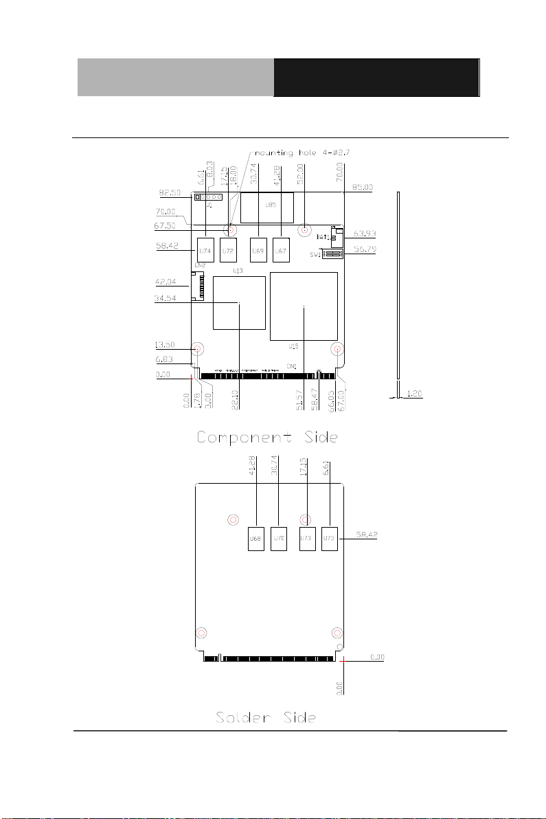
2.2 Location and Mechanical Drawing of Connectors and Jumpers
Chapter 2 Quick Installation Guide 2-3
Page 15

Qseven Module
A Q 7 - LN
Label
Function
SW1
AT_ATX Selection/Clear CMOS Setting
Label
Function
CN2
VGA Cable Connector
BAT1
RTC Battery Connector
2.3 List of Jumpers
The board has a number of jumpers/Connectors that allow you to
configure your system to suit your application.
The table below shows the function of each of the board's jumpers:
2.4 List of Connectors
The board has a number of connectors that allow you to configure your
system to suit your application. The table below shows the function of
each board's connectors:
Chapter 2 Quick Installation Guide 2-4
Page 16

Qseven Module
A Q 7 - LN
Pin
Signal
1
CRT_RED
2
CRT_GREEN
3
CRT_BLUE
4
GND
5
CRT_DDC_CLK
6
CRT_DDC_DATA
7
CRT_HSYNC
8
CRT_VSYNC
9
SMI#
10
SCI
Pin
Signal
1
+3V_BAT
2
GND
Pin
Signal
1
ON ->AT mode,OFF ->ATX mode (Default)
2
ON ->Clear CMOS,OFF ->reserve CMOS (Default)
Pin
Signal
Pin
Signal
1
GND
2
GND
3
GBE_MDI3-
4
GBE_MDI2-
2.5 VGA Connector (CN2)
2.6 RTC Battery Connector (BAT1)
2.7 CPLD Control Switch (SW1)
2.8 MXM Connector Pinout (CN1)
Chapter 2 Quick Installation Guide 2-5
Page 17

Qseven Module
A Q 7 - LN
5
GBE_MDI3+
6
GBE_MDI2+
7
GBE_LINK100#
8
GBE_LINK1000#
9
GBE_MDI1-
10
GBE_MDI0-
11
GBE_MDI1+
12
GBE_MDI0+
13
NC
14
GBE_ACT#
15
LAN_1.8V
16
SLP_S5#
17
WAKE#
18
SLP_S3#
19
SUS_STAT#
20
PWRBTN#
21
SLP_BTN#
22
LID_BTN#
23
GND
24
GND
KEY
KEY
25
GND
26
PWGIN
27
BATLOW#
28
RSTBTN#
29
SATA_TXP0
30
SATA_TXP1
31
SATA_TXN0
32
SATA_TXN1
33
ICH_SATA_LED#
34
GND
35
SATA_RXP0
36
SATA_RXP1
37
SATA_RXN0
38
SATA_RXN1
39
GND
40
GND
41
BIOS_DISABLE#
42
NC
43
NC
44
NC
45
NC
46
NC
47
NC
48
NC
49
NC
50
NC
51
NC
52
NC
53
NC
54
NC
55
NC
56
SMI#
57
GND
58
GND
Chapter 2 Quick Installation Guide 2-6
Page 18

Qseven Module
A Q 7 - LN
59
HDA_SYNC
60
SMBCLK
61
HDA_RST#
62
SMBDATA
63
HDA_BIT_CLK
64
SMBALERT#
65
HDA_SDIN0
66
NC
67
HDA_SDOUT
68
NC
69
NC
70
WDTRIG#
71
THERMTRIP#
72
WDT_OUT
73
GND
74
GND
75
USBP7N
76
USBP6N
77
USBP7P
78
USBP6P
79
OC#6_7
80
OC#4_5
81
USBP5N
82
USBP4N
83
USBP5P
84
USBP4P
85
OC#2_3
86
OC#0_1
87
USBP3N
88
USBP2N
89
USBP3P
90
USBP2P
91
NC
92
NC
93
USBP1N
94
USBP0N
95
USBP1P
96
USBP0P
97
GND
98
GND
99
LA_DATA0
100
NC
101
LA_DATA#0
102
NC
103
LA_DATA1
104
NC
105
LA_DATA#1
106
NC
107
LA_DATA2
108
NC
109
LA_DATA#2
110
NC
111
L_VDDEN
112
L_BKLTEN
113
NC
114
NC
Chapter 2 Quick Installation Guide 2-7
Page 19

Qseven Module
A Q 7 - LN
115
NC
116
NC
117
GND
118
GND
119
LA_CLK
120
NC
121
LA_CLK#
122
NC
123
L_BKLTCTL
124
NC
125
L_DDC_DATA
126
LCTLB_DATA
127
L_DDC_CLK
128
LCTLA_CLK
129
NC
130
NC
131
NC
132
NC
133
NC
134
NC
135
GND
136
GND
137
NC
138
NC
139
NC
140
NC
141
GND
142
GND
143
NC
144
NC
145
NC
146
NC
147
GND
148
GND
149
NC
150
NC
151
NC
152
NC
153
NC
154
NC
155
CLK_PCIE_100M
156
PCIE_WAKE#
157
CLK_PCIE_100M#
158
PCIE_RST#
159
GND
160
GND
161
ICH_PCIE_TXP3
162
ICH_PCIE_RXP3
163
ICH_PCIE_TXN3
164
ICH_PCIE_RXN3
165
GND
166
GND
167
ICH_PCIE_TXP2
168
ICH_PCIE_RXP2
169
ICH_PCIE_TXN2
170
ICH_PCIE_RXN2
Chapter 2 Quick Installation Guide 2-8
Page 20

Qseven Module
A Q 7 - LN
171
PCIE1_RST#
172
PCIE2_RST#
173
ICH_PCIE_TXP1
174
ICH_PCIE_RXP1
175
ICH_PCIE_TXN1
176
ICH_PCIE_RXN1
177
PCIE1_CPPE#
178
PCIE2_CPPE#
179
ICH_PCIE_TXP0
180
ICH_PCIE_RXP0
181
ICH_PCIE_TXN0
182
ICH_PCIE_RXN0
183
GND
184
GND
185
LPC_AD0
186
LPC_AD1
187
LPC_AD2
188
LPC_AD3
189
LPC_CLK
190
LPC_FRAME#
191
SERIRQ
192
LPC_LDRQ#0
193
RTCBAT
194
ICH_SPKR
195
FAN_TAC
196
FAN_CTL
197
GND
198
GND
199
SPI_SI
200
SPI_CS#0
201
SPI_SO
202
NC
203
SPI_CLK
204
NC
205
+5VSB_EXT
206
+5VSB_EXT
207
TCK_M
208
TDO_M
209
TMS_M
210
TDI_M
211
+5V_EXT
212
+5V_EXT
213
+5V_EXT
214
+5V_EXT
215
+5V_EXT
216
+5V_EXT
217
+5V_EXT
218
+5V_EXT
219
+5V_EXT
220
+5V_EXT
221
+5V_EXT
222
+5V_EXT
223
+5V_EXT
224
+5V_EXT
225
+5V_EXT
226
+5V_EXT
Chapter 2 Quick Installation Guide 2-9
Page 21

Qseven Module
A Q 7 - LN
227
+5V_EXT
228
+5V_EXT
229
+5V_EXT
230
+5V_EXT
Chapter 2 Quick Installation Guide 2-10
Page 22

Qseven Module
A Q 7 - LN
部件名称
有毒有害物质或元素
铅
(Pb)
汞
(Hg) 镉 (Cd)
六价铬
(Cr(VI))
多溴联苯
(PBB)
多溴二苯醚
(PBDE)
印刷电路板
及其电子组件
× ○ ○ ○ ○
○
外部信号
连接器及线材
× ○ ○ ○ ○
○
O:表示该有毒有害物质在该部件所有均质材料中的含量均在
SJ/T 11363-2006 标准规定的限量要求以下。
X:表示该有毒有害物质至少在该部件的某一均质材料中的含量超出
SJ/T 11363-2006 标准规定的限量要求。
备注:此产品所标示之环保使用期限,系指在一般正常使用状况下。
Below Table for China RoHS Requirements
产品中有毒有害物质或元素名称及含量
AAEON Main Board/ Daughter Board/ Backplane
Chapter 2 Quick Installation Guide 2-11
Page 23

Qseven Module
A Q 7 - LN
Chapter
3
AMI
BIOS Setup
Chapter 3 AMI BIOS Setup 3-1
Page 24

Qseven Module
A Q 7 - LN
3.1 System Test and Initialization
These routines test and initialize board hardware. If the routines
encounter an error during the tests, you will either hear a few short
beeps or see an error message on the screen. There are two kinds
of errors: fatal and non-fatal. The system can usually continue the
boot up sequence with non-fatal errors.
System configuration verification
These routines check the current system configuration against the
values stored in the CMOS memory. If they do not match, the
program outputs an error message. You will then need to run the
BIOS setup program to set the configuration information in memory.
There are three situations in which you will need to change the
CMOS settings:
1. You are starting your system for the first time
2. You have changed the hardware attached to your system
3. The CMOS memory has lost power and the configuration
information has been erased.
The AQ7-LN CMOS memory has an integral lithium battery backup
for data retention. However, you will need to replace the complete
unit when it finally runs down.
Chapter 3 AMI BIOS Setup 3-2
Page 25

Qseven Module
A Q 7 - LN
3.2 AMI BIOS Setup
AMI BIOS ROM has a built-in Setup program that allows users to
modify the basic system configuration. This type of information is
stored in battery-backed CMOS RAM so that it retains the Setup
information when the power is turned off.
Entering Setup
Power on the computer and press <Del> or <F2> immediately. This
will allow you to enter Setup.
Main
Set the date, use tab to switch between date elements.
Advanced
Enable disable boot option for legacy network devices.
Chipset
Host bridge parameters.
Boot
Enables/disable quiet boot option.
Security
Set setup administrator password.
Save&Exit
Exit system setup after saving the changes.
Chapter 3 AMI BIOS Setup 3-3
Page 26

Qseven Module
A Q 7 - LN
Setup Menu
Main
Chapter 3 AMI BIOS Setup 3-4
Page 27

Qseven Module
A Q 7 - LN
Launch PXE OpROM
Enable
Optimal Default, Failsafe
Default
Disable
Enable or Disable Boot Option for Legacy Network Devices
Advanced
Options Summary:
Chapter 3 AMI BIOS Setup 3-5
Page 28

Qseven Module
A Q 7 - LN
PCI Latency
Timer
32 PCI Bus Clocks
Optimal Default, Failsafe Default
64 PCI Bus Clocks
96 PCI Bus Clocks
128 PCI Bus Clocks
160 PCI Bus Clocks
192 PCI Bus Clocks
224 PCI Bus Clocks
248 PCI Bus Clocks
Value to be programmed into PCI Latency Timer Register.
PCI Subsystem Settings
Options Summary:
Chapter 3 AMI BIOS Setup 3-6
Page 29

Qseven Module
A Q 7 - LN
Enable ACPI Auto
Configuration
Enable
Disable
Optimal Default, Failsafe
Default
Enables or Disables BIOS ACPI Auto Configuration
Enable Hibernation
Enable
Optimal Default, Failsafe
Default
Disable
Enables or Disables System ability to Hibernate (OS/S4 Sleep State).
This option may be not effective with some OS
ACPI Settings
Options Summary:
Chapter 3 AMI BIOS Setup 3-7
Page 30

Qseven Module
A Q 7 - LN
Suspend mode
Suspend Disabled
S1 (CPU Stop Clock)
S3 (Suspend to RAM)
Optimal Default, Failsafe
Default
Select the ACPI state used for System Suspend
Chapter 3 AMI BIOS Setup 3-8
Page 31

Qseven Module
A Q 7 - LN
Intel SpeedStep
Enable
Optimal Default, Failsafe
Default
Disable
Enable or Disable Intel(R) SpeedStep(tm)
Hyper-Threading
Enable
Optimal Default, Failsafe
Default
Disable
En/Disable CPU Hyper-Threading function
CPU Configuration
Options Summary:
Chapter 3 AMI BIOS Setup 3-9
Page 32

Qseven Module
A Q 7 - LN
Execute Disable
Bit
Enable
Optimal Default, Failsafe
Default
Disable
Execute Disable can prevent certain classes of malicious buffer overflow
attacks when combined with a supporting OS (Windows Server 2003
SP1, Windows XP SP2, SuSE Linux 9.2, RedHat Enterprise 3 Update 3.)
Limit CPUID
Maximum
Enable
Optimal Default, Failsafe
Default
Disable
Disabled for Windows XP
Chapter 3 AMI BIOS Setup 3-10
Page 33

Qseven Module
A Q 7 - LN
ATA Or IDE Configuration
Compatible
Optimal Default,
Failsafe Default
Enhanced
Select ATA or IDE configuration
Configure SATA As
IDE
Optimal Default,
Failsafe Default
RAID
AHCI
Select a configuration for SATA controller
IDE Configuration
Options Summary:
Chapter 3 AMI BIOS Setup 3-11
Page 34

Qseven Module
A Q 7 - LN
DVMT Mode Select
Fixed Mode
DVMT Mode
Optimal Default, Failsafe
Default
Select DVMT Mode used by Internal Graphics Device
DVMT/FIXED
Memory
128MB
256MB
Optimal Default, Failsafe
Default
Maximum
Intel IGD SWSCI OpRegion
Options Summary:
Chapter 3 AMI BIOS Setup 3-12
Page 35

Qseven Module
A Q 7 - LN
Select DVMT/FIXED Mode Memory size used by Internal Graphics
Device
IGD – Boot Type
CRT
LFP
CRT + LFP
Optimal Default, Failsafe
Default
Select the Video Device which will be activated during POST. This has
no effect if external graphics present
LCD Panel Type
640x480 LVDS
800x600 LVDS
1024x768 LVDS
Optimal Default, Failsafe
Default
800x480 LVDS
1280x768 LVDS
1280x800 LVDS
Select LCD panel used by Internal Graphics Device by selecting the
appropriate setup item
Backlight control
function
The Most Bright
100%
A Little Bright
75%
The Medium Light
50%
Optimal Default, Failsafe
Default
Chapter 3 AMI BIOS Setup 3-13
Page 36

Qseven Module
A Q 7 - LN
A Little Dark
25%
The Most Dark
0%
Select Backlight brightness of LVDS
Chapter 3 AMI BIOS Setup 3-14
Page 37

Qseven Module
A Q 7 - LN
Legacy USB Support
Enabled
Optimal Default,
Failsafe Default
Disabled
Auto
Enables BIOS Support for Legacy USB Support. When enabled, USB can
be functional in legacy environment like DOS.
AUTO option disables legacy support if no USB devices are connected
Device Name (Emulation
Type)
Auto
Optimal Default,
Failsafe Default
USB Configuration
Options Summary:
Chapter 3 AMI BIOS Setup 3-15
Page 38

Qseven Module
A Q 7 - LN
Floppy
Forced FDD
Hard Disk
CDROM
If Auto. USB devices less than 530MB will be emulated as Floppy and
remaining as Floppy and remaining as hard drive. Forced FDD option can
be used to force a HDD formatted drive to boot as FDD(Ex. ZIP drive)
Chapter 3 AMI BIOS Setup 3-16
Page 39

Qseven Module
A Q 7 - LN
W83L786G H/W Monitor
Chapter 3 AMI BIOS Setup 3-17
Page 40

Qseven Module
A Q 7 - LN
Super IO Configuration
Chapter 3 AMI BIOS Setup 3-18
Page 41

Qseven Module
A Q 7 - LN
Serial Port 0 Configuration
Chapter 3 AMI BIOS Setup 3-19
Page 42

Qseven Module
A Q 7 - LN
Serial Port
Disabled
Enabled
Optimal Default, Failsafe Default
Allows BIOS to En/Disable correspond serial port.
Change Settings
(Serial Port 1)
Auto
Optimal Default, Failsafe Default
IO=3F8h; IRQ=4;
IO=3F8h; IRQ=3,4;
IO=2F8h; IRQ=3,4;
IO=3E8h;
IRQ=10,11;
Serial Port 1 Configuration
Options summary:
Chapter 3 AMI BIOS Setup 3-20
Page 43

Qseven Module
A Q 7 - LN
IO=2E8h;
IRQ=10,11
Allows BIOS to Select Serial Port resource.
Change Settings
(Serial Port 2)
Auto
Optimal Default, Failsafe Default
IO=2F8h; IRQ=3;
IO=3F8h; IRQ=3,4;
IO=2F8h; IRQ=3,4;
IO=3E8h;
IRQ=10,11;
IO=2E8h;
IRQ=10,11
COM2 Type Select
RS232
Optimal Default, Failsafe Default
RS422
RS485
Allows BIOS to Select Serial Port resource.
Chapter 3 AMI BIOS Setup 3-21
Page 44

Qseven Module
A Q 7 - LN
Port 1-8
Input
Output
Set GPIO as Input or Output
Digital IO Port Configuration
Options summary:
Chapter 3 AMI BIOS Setup 3-22
Page 45

Qseven Module
A Q 7 - LN
PLL1 Spread Spectrum
Disable
Enable
Optimal Default,
Failsafe Default
Spread Spectrum Setting for PLL1
PLL3 Spread Spectrum
Disable
Enable
Optimal Default,
Failsafe Default
Spread Spectrum Setting for PLL3
Clock Generator Configuration
Options summary:
Chapter 3 AMI BIOS Setup 3-23
Page 46

Qseven Module
A Q 7 - LN
Chipset
Chapter 3 AMI BIOS Setup 3-24
Page 47

Qseven Module
A Q 7 - LN
MMIO Size
AUTO
Optimal Default,
Failsafe Default
1GB
2GB
Set reserve memory size for MMIO
Initiate Graphic Adapter
IGD
Optimal Default,
Failsafe Default
Select which graphics controller to use as the primary boot device.
Host Bridge
Options summary:
Chapter 3 AMI BIOS Setup 3-25
Page 48

Qseven Module
A Q 7 - LN
Memory Frequency and Timing
Chapter 3 AMI BIOS Setup 3-26
Page 49

Qseven Module
A Q 7 - LN
Share Memory Size
1 MB
8 MB
Select Share Memory Size
OnChip VGA Configuration
Options summary:
Chapter 3 AMI BIOS Setup 3-27
Page 50

Qseven Module
A Q 7 - LN
HD Audio Controller
Disabled
Enable
Optimal Default,
Failsafe Default
Enabling/Disabling HD Audio controller.
USB Function
Disabled
Enabled
Optimal Default,
Failsafe Default
Enabling/Disabling 8111E controller
South Bridge
Options Summary:
Chapter 3 AMI BIOS Setup 3-28
Page 51

Qseven Module
A Q 7 - LN
USB 2.0(EHCI) Support
Disabled
Enabled
Optimal Default,
Failsafe Default
Enable or disable USB 2.0 (EHCI) Support
SMBus Controller
Disabled
Enabled
Optimal Default,
Failsafe Default
Enable or disable onchip SMBus Controller
LAN1(i82567V Gbe
Controller)
Disabled
Enabled
Optimal Default,
Failsafe Default
Enable or disable onchip GbE Controller
LAN2(i82574L Gbe
Controller)
Disabled
Enabled
Optimal Default,
Failsafe Default
Enable / Disable onboard i82574L Ethernet Controller
PCI Express Root Port x
Disabled
Enabled
Auto
Optimal Default,
Failsafe Default
Enabling/Disabling PCI Express root ports
Chapter 3 AMI BIOS Setup 3-29
Page 52

Qseven Module
A Q 7 - LN
SLP_S4 Assertion Width
1-2 Seconds
2-3 Seconds
3-4 Seconds
Optimal Default,
Failsafe Default
4-5 Seconds
Select a minimum assertion width of the SLP_S4# signal
Restore on AC Power
Loss
Power Off
Optimal Default,
Failsafe Default
Power On
Last State
Select the action system to take when restoring from power loss.
Chapter 3 AMI BIOS Setup 3-30
Page 53

Qseven Module
A Q 7 - LN
Bootup NumLock
State
On
Optimal Default, Failsafe Default
Off
Select the keyboard NumLock state
Quiet Boot
Disabled
Enabled
Optimal Default, Failsafe Default
En/Disable showing boot logo.
GateA20 Active
Upon Request
Optimal Default, Failsafe Default
Always
Boot
Options Summary:
Chapter 3 AMI BIOS Setup 3-31
Page 54

Qseven Module
A Q 7 - LN
UPON REQUEST - GA20 can be disabled using BIOS services. ALWAYS
- do not allow disabling GA20; this option is useful when any RT code is
executed above 1MB.
Option ROM
Messages
Force BIOS
Optimal Default, Failsafe Default
Keep Current
Set display mode for Option ROM
Chapter 3 AMI BIOS Setup 3-32
Page 55

Qseven Module
A Q 7 - LN
Security
Change User/Supervisor Password
You can install a Supervisor password, and if you install a
supervisor password, you can then install a user password. A user
password does not provide access to many of the features in the
Setup utility.
If you highlight these items and press Enter, a dialog box appears
which lets you enter a password. You can enter no more than six
letters or numbers. Press Enter after you have typed in the
password. A second dialog box asks you to retype the password
for confirmation. Press Enter after you have retyped it correctly.
The password is required at boot time, or when the user enters the
Chapter 3 AMI BIOS Setup 3-33
Page 56

Qseven Module
A Q 7 - LN
Setup utility.
Removing the Password
Highlight this item and type in the current password. At the next
dialog box press Enter to disable password protection.
Save & Exit
Chapter 3 AMI BIOS Setup 3-34
Page 57

Qseven Module
A Q 7 - LN
Chapter
4
Driver
Installation
Chapter 4 Driver Installation 4-1
Page 58

Qseven Module
A Q 7 - LN
The AQ7-LN comes with a CD-ROM that contains all drivers and
utilities that meet your needs.
Follow the sequence below to install the drivers:
Step 1 – Install Chipset Driver
Step 2 – Install VGA Driver
Step 3 – Install Audio Driver
Step 4 – Install LAN Driver
Step 5 – Install Touch Panel Driver
Please read instructions below for further detailed installations.
Chapter 4 Driver Installation 4-2
Page 59

Qseven Module
A Q 7 - LN
4.1 Installation:
Insert the AQ7-LN CD-ROM into the CD-ROM Drive. And install the
drivers from Step 1 to Step 5 in order.
Step 1 – Install Chipset Driver
1. Click on the STEP1-CHIPSET folder and select the folder
of OS your system is
2. Double click on the infinst_autol.exe located in each OS
folder
3. Follow the instructions that the window shows
4. The system will help you install the driver automatically
Step 2 – Install VGA Driver
1. Click on the STEP2-VGA folder and select the folder of
OS your system is
2. Double click on the Setup.exe file located in each OS
folder
3. Follow the instructions that the window shows
4. The system will help you install the driver automatically
Step 3 – Install Audio Driver
1. Click on the STEP3-AUDIO folder and select the folder of
OS your system is
2. Double click on the .exe file located in each OS folder
3. Follow the instructions that the window shows
4. The system will help you install the driver automatically
Chapter 4 Driver Installation 4-3
Page 60

Qseven Module
A Q 7 - LN
Step 4 – Install LAN Driver
1. Click on the STEP4-LAN folder and select the folder of
OS your system is
2. Double click on the .exe file located in each OS folder
3. Follow the instructions that the window shows
4. The system will help you install the driver automatically
Step 5 – Install Touch Panel Driver
1. Click on the STEP5-TOUCH PANEL folder and select the
folder of OS your system is
2. Double click on the Setup.exe file located in each OS
folder
3. Follow the instructions that the window shows
4. The system will help you install the driver automatically
Chapter 4 Driver Installation 4-4
Page 61

Qseven Module AQ7-LN
A
Appendix
Programming the
Watchdog Timer
Appendix A Programming the Watchdog Timer A-1
Page 62

Qseven Module AQ7-LN
A.1 Programming
AQ7-LN utilizes W83627DHG-P chipset as its watchdog timer
controller.
Below are the procedures to complete its configuration and the
AAEON intial watchdog timer program is also attached based on
which you can develop customized program to fit your application.
Configuring Sequence Description
Unlock W83627DHG
Select register of
watchdog timer
Enable the function of
the watchdog timer
Use the function of the
watchdog timer
Lock W83627DHG
There are three steps to complete the configuration setup:
(1) Enter the W83627DHG config Mode
(2) Modify the data of configuration registers
Appendix A Programming the Watchdog Timer A-2
Page 63

Qseven Module AQ7-LN
(3) Exit the W83627DHG config Mode. Undesired result may
occur if the config Mode is not exited normally.
(1) Enter the W83627DHG config Mode
To enter the W83627DHG config Mode, two special I/O write
operations are to be performed during Wait for Key state. To
ensure the initial state of the key-check logic, it is necessary to
perform two write operations to the Special Address port (2EH).
The different enter keys are provided to select configuration ports
(2Eh/2Fh) of the next step.
Address Port Data Port
87h,87h: 2Eh 2Fh
(2) Modify the Data of the Registers
All configuration registers can be accessed after entering the config
Mode. Before accessing a selected register, the content of Index
07h must be changed to the LDN to which the register belongs,
except some Global registers.
(3) Exit the W83627DHG config Mode
The exit key is provided to select configuration ports (2Eh/2Fh) of
the next step.
Address Port Data Port
0aah: 2Eh 2Fh
WatchDog Timer Register I (Index=F5h, Default=00h)
CRF5 (PLED and KBC P20 Control Mode Register)
Bit 7-5 : select PLED mode
= 000 Power LED pin is driven high.
= 001 Power LED pin outputs 0.5Hz pulse
with 50% duty cycle.
Appendix A Programming the Watchdog Timer A-3
Page 64

Qseven Module AQ7-LN
= 010 Power LED pin is driven low.
= 011 Power LED pin outputs 2Hz pulse
with 50% duty cycle.
= 100 Power LED pin outputs 1Hz pulse
with 50% duty cycle.
= 101 Power LED pin outputs 4Hz pulse
with 50% duty cycle.
= 110 Power LED pin outputs 0.25Hz pulse
with 50% duty cycle.
=111 Power LED pin outputs 0.25Hz pulse
with 50% duty cycle..
Bit 4 : WDTO# count mode is 1000 times faster.
= 0 Disable.
= 1 Enable.
Bit 3 : select WDTO# count mode.
= 0 second
= 1 minute
Bit 2 : Enable the rising edge of keyboard Reset
(P20) to force Time-out event.
= 0 Disable
= 1 Enable
Bit 1 : Disable / Enable the WDTO# output low
pulse to the KBRST# pin (PIN60)
= 0 Disable
= 1 Enable
Bit 0 : Reserved.
Appendix A Programming the Watchdog Timer A-4
Page 65

Qseven Module AQ7-LN
WatchDog Timer Register II (Index=F6h, Default=00h)
Bit 7-0 = 0 x 00 Time-out Disable
= 0 x 01 Time-out occurs after 1
second/minute
= 0 x 02 Time-out occurs after 2
second/minutes
= 0 x 03 Time-out occurs after 3
second/minutes
………………………………..
= 0 x FF Time-out occurs after 255
second/minutes
WatchDog Timer Register III (Index=F7h, Default=00h)
Bit 7 : Mouse interrupt reset Enable or Disable
= 1 Watchdog Timer is reset upon a
Mouse interrupt
= 0 Watchdog Timer is not affected by
Mouse interrupt
Bit 6 : Keyboard interrupt reset Enable or
Disable
= 1 Watchdog Timer is reset upon a
Keyboard interrupt
= 0 Watchdog Timer is not affected by
Keyboard interrupt
Bit 5 : Force Watchdog Timer Time-out. Write
Only
Appendix A Programming the Watchdog Timer A-5
Page 66

Qseven Module AQ7-LN
= 1 Force Watchdog Timer time-out
event: this bit is self-clearing
Bit 4 : Watchdog Timer Status. R/W
= 1 Watchdog Timer time-out occurred
= 0 Watchdog Timer counting
Bit 3-0 : These bits select IRQ resource for
Watchdog. Setting of 2 selects SMI.
Appendix A Programming the Watchdog Timer A-6
Page 67

Qseven Module AQ7-LN
A.2 W83627DHG Watchdog Timer Initial Program
Example: Setting 10 sec. as Watchdog timeout interval
;///////////////////////////////////////////////////////////////////////////////////////////////
Mov dx,2eh ;Enter W83627DHG config mode
Mov al,87h (out 87h to 2eh twice)
Out dx,al
Out dx,al
;///////////////////////////////////////////////////////////////////////////////////////////////
Mov al,07h
Out dx,al
Inc dx
Mov al,08h ;Select Logical Device 8 (GPIO Port
2)
Out dx,al
;///////////////////////////////////////////////////////////////////////////////////////////////
Dec dx
Mov al,30h ;CR30 (GP20~GP27)
Out dx,al
Inc dx
Mov al,01h ;Activate GPIO2
Out dx,al
Appendix A Programming the Watchdog Timer A-7
Page 68

Qseven Module AQ7-LN
;///////////////////////////////////////////////////////////////////////////////////////////////
Dec dx
Mov al,0f5h ;CRF5 (PLED mode register)
Out dx,al
Inc dx
In al,dx
And al,not 08h ;Set second as counting unit
Out dx,al
;///////////////////////////////////////////////////////////////////////////////////////////////
Dec dx
Mov al,0f6h ; CRF6
Out dx,al
Inc dx
Mov al,10 ;Set timeout interval as 10 sec.
Out dx,al
;///////////////////////////////////////////////////////////////////////////////////////////////
Dec dx ;Exit W83627DHG config mode
Mov al,0aah (out 0aah to 2eh once)
Out dx,al
;///////////////////////////////////////////////////////////////////////////////////////////////
Appendix A Programming the Watchdog Timer A-8
Page 69

Qseven Module AQ7-LN
Appendix
B
I/O Information
Appendix B I/O Information B - 1
Page 70

Qseven Module AQ7-LN
B.1 I/O Address Map
Appendix B I/O Information B - 2
Page 71

Qseven Module AQ7-LN
B.2 1st MB Memory Address Map
Appendix B I/O Information B - 3
Page 72

Qseven Module AQ7-LN
B.3 IRQ Mapping Chart
B.4 DMA Channel Assignments
Appendix B I/O Information B - 4
 Loading...