

ZMD SAP5S, SAP51 Datasheet

SAP5S / SAP51
Revision C
DSTBn
LED1
OSC2
OSC1
P1
P0
D1
D0
P2
P3
D2
D3
PSTBn
LED2
PFAULT
UOUT
U5R
LTGN
CDC
LTGP
DSTBn
LED1
OSC2
OSC1
D1D0D2
D3
PSTBn
LED2
PFAULT
UOUT
U5R
LTGN
CDC
LTGP
Universal Actuator-Sensor Interface IC
Datasheet
Features
Universal application in AS-i Slave, Mas-
•
ter, Repeater and Bus-Monitor components
Support of AS-i Complete Specification
•
V3.0, including all optional features
Synchronous Data I/O Mode
-
-
4 Input / 4 Output operation in
Extended Address Mode
-
User write protection for
Extended ID-Code 1
-
Multiplexed Parameter Port
Full support of the AS-i “Safety at Work”
•
concept
On chip electronic inductor with current
•
drive capability of 55mA
LED outputs supporting all status indica-
•
tion modes defined by AS-i Complete
Specification V3.0
Data preprocessing functions: input filter-
•
ing and input inverting
Support of 5.33 / 16 MHz crystals by auto-
•
matic frequency detection
Clock Watchdog for high System Security
•
Communication Watchdog
•
Description
SAP5 is a monolithic CMOS integrated circuit
certified for AS-i (Actuator Sensor Interface)
networks. AS-i networks are used for industrial
automation.
AS-i is designed for easy and simple interconnection of binary sensors and actuators. It
uses a two-wire unshielded cable to transport
power and information.
Using the SAP5 safety-related AS-i slaves can
be realized according to the AS-i “Safety at
Work” concept. Slaves complying with category 4 of EN954-1 can be realized with a
minimum of external circuitry.
The device is available in SOP20 and SOP16
package.
Application Support
Configuration of the chip is handled through
programming of the on-chip E²PROM. ZMD
provides special tools to ease product evaluation and selection of different operation modes.
AS-Interface Programmer 2.0 USB
(Ordering Code: 3600100145)
SAP5 Evaluation Board 2.0
(Ordering Code: 3600100144)
Further application support is available through
e-mail hotline under asi@zmd.de
SAP5
Rev. 2.0 Copyright © 2007, ZMD AG
All rights reserved. The material contained herein may not be reproduced, adapted, merged, translated, stored, or used without the prior written consent of the copyright owner. The
Information furnished in this publication is preliminary and subject to changes without notice.
SAP5
1/58

Datasheet
ZENTRUM MIKROELEKTRONIK DRESDEN AG
SAP5S / SAP51
Table of Contents
0 READ THIS FIRST ...........................................................................................................................................4
0.1 I
0.2 R
0.3 R
1 GENERAL DEVICE SPECIFICATION.............................................................................................................5
1.1 A
1.2 O
1.3 EMC B
1.4 Q
1.5 F
1.6 H
1.7 P
2 BASIC FUNCTIONAL DESCRIPTION ..........................................................................................................10
2.1 F
2.2 G
2.3 S
3 E²PROM .........................................................................................................................................................17
3.1 O
3.2 U
3.3 F
3.4 S
4 DETAILED FUNCTIONAL DESCRIPTION ...................................................................................................23
4.1 P
4.2 T
4.3 DC C
4.4 DC C
4.5 AS-I R
4.6 AS-I T
4.7 P
4.8 D
4.9 D
4.10
4.11
MPORTANT NOTICE
EFERENCES
EVISION HISTORY
BSOLUTE MAXIMUM RATINGS (NON OPERATING
PERATING CONDITIONS
UALITY STANDARDS
AILURE RATE
UMIDITY CLASS
ACKAGE PIN ASSIGNMENT
UNCTIONAL BLOCK DIAGRAM
ENERAL OPERATIONAL MODES
LAVE MODE
2.3.1 AS-i communication channel ...........................................................................................................12
2.3.2 Parameter Port Pins.........................................................................................................................12
2.3.3 Data Port Pins ..................................................................................................................................13
2.3.4 Data Input Inversion .........................................................................................................................13
2.3.5 Data Input Filtering...........................................................................................................................13
2.3.6 Synchronous Data I/O Mode............................................................................................................13
2.3.7 4 Input / 4 Output processing in Extended Address Mode ..............................................................13
2.3.8 AS-i Safety Mode .............................................................................................................................14
2.3.9 Enhanced LED Status Indication .....................................................................................................14
2.3.10 Communication Monitor/Watchdog ..................................................................................................14
2.3.11 Write protection of ID_Code_Extension_1 .......................................................................................14
2.3.12 Summary of Master Calls.................................................................................................................14
VERVIEW
SER AREA PROGRAMMING
IRMWARE AREA PROGRAMMING
AFETY AREA PROGRAMMING
OWER SUPPLY
4.1.1 Voltage Output Pins UOUT and U5R...............................................................................................23
4.1.2 Input Impedance (AS-i bus load) .....................................................................................................24
HERMAL PROTECTION
HARACTERISTICS
HARACTERISTICS
ECEIVER
RANSMITTER
ARAMETER PORT AND
ATA PORT AND
4.8.1 Timing of Data I/O and DSTBn ........................................................................................................28
4.8.2 Input Data Pre-Processing ...............................................................................................................29
4.8.3 Synchronous Data I/O Mode............................................................................................................30
4.8.4 Support of 4I/4O Signaling in Extended Address Mode ..................................................................31
4.8.5 Special function of DSTBn ...............................................................................................................33
ATA AND PARAMETER PORT CONFIGURATION
F
AULT INDICATION INPUT
LED
..............................................................................................................................................4
EHAVIOR
.............................................................................................................................................7
.............................................................................................................................................12
................................................................................................................................................17
..........................................................................................................................................26
OUTPUTS
.....................................................................................................................................4
......................................................................................................................................4
) ........................................................................................5
.............................................................................................................................6
..........................................................................................................................................6
..................................................................................................................................6
.........................................................................................................................................7
..........................................................................................................................8
....................................................................................................................10
................................................................................................................12
.......................................................................................................................17
...............................................................................................................20
....................................................................................................................21
........................................................................................................................................23
..............................................................................................................................24
– D
IGITAL INPUTS
– D
IGITAL OUTPUTS
....................................................................................................................................26
PSTBN.................................................................................................................27
DSTBN............................................................................................................................28
PFAULT .........................................................................................................34
.......................................................................................................................................34
...................................................................................................25
................................................................................................25
...........................................................................................33
Page
Rev. 2.0, Copyright © 2007, ZMD AG
All rights reserved. The material contained herein may not be reproduced, adapted, merged, translated, stored, or used without the prior written consent of the copyright owner. The
Information furnished in this publication is preliminary and subject to changes without notice.
2/58

Datasheet
4.11.1 Slave Mode ......................................................................................................................................34
4.11.2 Master/Repeater Mode ....................................................................................................................35
4.12
4.13
4.13.1 Power On Reset...............................................................................................................................36
4.13.2 Logic controlled Reset .....................................................................................................................37
4.13.3 External Reset .................................................................................................................................37
4.14
4.15
4.16
4.17
4.18
4.19
4.19.1 Master/ Repeater Mode Activation ..................................................................................................45
4.19.2 Pin Assignment ................................................................................................................................45
4.19.3 Functional Description .....................................................................................................................47
4.20
5 APPLICATION CIRCUITS .............................................................................................................................51
6 PACKAGE OUTLINES ..................................................................................................................................54
7 PACKAGE MARKING ...................................................................................................................................55
8 ORDERING INFORMATION..........................................................................................................................56
9 CONTACT INFORMATION ...........................................................................................................................57
9.1 ZMD S
9.2 ZMD D
9.3 AS-I
O
IC R
UART ...................................................................................................................................................39
M
S
C
S
M
W
SCILLATOR PINS
ESET
..............................................................................................................................................36
AIN STATE MACHINE
TATUS REGISTERS
OMMUNICATION MONITOR/WATCHDOG
AFETY MODE
ASTER- AND REPEATER MODE
RITE PROTECTION OF
ALES CONTACTS
ISTRIBUTION PARTNERS
NTERNATIONAL ASSOCIATION
.......................................................................................................................................41
ZENTRUM MIKROELEKTRONIK DRESDEN AG
SAP5S / SAP51
OSC1, OSC2 ...........................................................................................................36
............................................................................................................................40
...............................................................................................................................40
.................................................................................................40
.............................................................................................................45
ID_C
ODE_EXTENSION
.............................................................................................................................57
..................................................................................................................57
..............................................................................................................57
_1 ...................................................................................49
Rev. 2.0, Copyright © 2007, ZMD AG
All rights reserved. The material contained herein may not be reproduced, adapted, merged, translated, stored, or used without the prior written consent of the copyright owner. The
Information furnished in this publication is preliminary and subject to changes without notice.
3/58

Datasheet
ZENTRUM MIKROELEKTRONIK DRESDEN AG
SAP5S / SAP51
0 Read this First
0.1 Important Notice
Products sold by ZMD are covered exclusively by the warranty, patent indemnification and other provisions appearing in ZMD standard "Terms of Sale". ZMD makes no warranty (express, statutory, implied and/or by description), including without limitation any warranties of merchantability and/or fitness for a particular purpose,
regarding the information set forth in the Materials pertaining to ZMD products, or regarding the freedom of any
products described in the Materials from patent and/or other infringement. ZMD reserves the right to discontinue
production and change specifications and prices of its products at any time and without notice. ZMD products
are intended for use in commercial applications. Applications requiring extended temperature range, unusual
environmental requirements, or high reliability applications, such as military, medical life-support or lifesustaining equipment, are specifically not recommended without additional mutually agreed upon processing by
ZMD for such applications.
ZMD reserves the right to change the detail specifications as may be required to permit improvements in the
design of its products.
0.2 References
[1] AS-Interface Complete Specification Version 3.0, dated 16.09.2004
[2] Spezifikation der sicheren AS-i-Übertragung, Leuze electronic, 12.05.2000
0.3 Revision History
Revision Date Technical Changes Page in Datasheet
B September 2005 First marketed silicon version
C March 2007 Modified I
C March 2007 Modified Delay Mode activation through pa-
rameter port P1
C March 2007 Modified Synchronous Data I/O Mode activation
through parameter port P2
C March 2007 Modified Watchdog activation through parame-
ter port P0
C March 2007 Improved Burst protection filter and improved
ESD behavior
– current range for input low level Table 16 at Page 25
IL
Page 29
Page 30
Page 40
Rev. 2.0, Copyright © 2007, ZMD AG
All rights reserved. The material contained herein may not be reproduced, adapted, merged, translated, stored, or used without the prior written consent of the copyright owner. The
Information furnished in this publication is preliminary and subject to changes without notice.
4/58

Datasheet
ZENTRUM MIKROELEKTRONIK DRESDEN AG
SAP5S / SAP51
1 General Device Specification
1.1 Absolute Maximum Ratings (Non Operating)
Table 1: Absolute Maximum Ratings
Symbol Parameter Min Max Unit Note
V
Voltage reference 0 0 V
LTGN
V
LTGP-LTGN
V
LTGP-LTGN_P
V
inputs1
Voltage difference between LTGP and LTGN (V
V
)
LTGN
Pulse voltage between LTGP and LTGN (V
LTGP
- V
-
LTGP
) 0 50 V
LTGN
Voltage at pin CDC, D0…D3, P0…P3, DSTBn, PSTBnBn,
0 40 V
-0.3 V
+ 0.3 V
UOUT
LED1, LED2, PFAULT, UOUT
V
Voltage at pins OSC1, OSC2, U5R -0.3 7 V
inputs2
Iin Input current into any pin except supply pins -50 50 mA
H Humidity non-condensing
V
Electrostatic discharge – Human Body Model (HBM2) 1500 V
HBM
V
Electrostatic discharge – Equipment Discharge Model
EDM
200 V
(EDM)
θ
STG
θ
lead
θ
lead
R
Thermal resistance of SOIC 16 package 80 100 K/W
thj-16
R
Thermal resistance of SOIC 20 package 75 95 K/W
thj-20
1
reverse polarity protection has to be performed externally,
2
pulse with ≤ 50µs, repetition rate ≤ 0.5 Hz
3
V
LTGP-LTGN
4
Latch-up resistance, reference pin is 0V
5
Level 4 according to JEDEC-020A is guaranteed
6
HBM: C = 100pF charged to V
7
EDM: C = 200pF charged to V
8
Single layer board, P
Storage temperature -55 125 °C
JEDEC-J-STD-020C
Soldering temperature Sn/Pb
Soldering temperature 100%Sn
and V
LTGP-LTGN_P
tot
must not be violated
with resistor R = 1.5kΩ in series, valid for all pins except LTGP-LTGN
HBM2
with no resistor in series, valid for LTGP-LTGN only
EDM
= 0.5W; air velocity = 0m/s ⇒ max. value; air velocity = 2.5m/s ⇒ min. value
JEDEC-J-STD-020C
240
260
°C
°C
1
2
4
5
6
7
8
8
Rev. 2.0, Copyright © 2007, ZMD AG
All rights reserved. The material contained herein may not be reproduced, adapted, merged, translated, stored, or used without the prior written consent of the copyright owner. The
Information furnished in this publication is preliminary and subject to changes without notice.
5/58

Datasheet
ZENTRUM MIKROELEKTRONIK DRESDEN AG
SAP5S / SAP51
1.2 Operating Conditions
Table 2: Operating Conditions
Symbol Parameter Min Max. Unit Note
V
Negative supply voltage 0 0 V
LTGN
V
DC voltage at LTGP relating to V
LTGP
I
Operating current at V
LTGP
I
Max. output sink current at pins D3...D0, DSTBn 10 mA
CL1
I
Max. output sink current at pins P0...P3, PSTBnBn 10 mA
CL2
θ
amb
1
Below V
Ambient temperature range, operating range -25 85 °C
the power supply block may not be able to provide the specified output currents at
LTGPmin
= 30V 6 mA
UIN
16 34 V
LTGN
UOUT and U5R.
2
Outside of these limits the send current shape and send current amplitude cannot be guaranteed.
3
fc = 16.000 MHz, no load at any pin, transmitter turned off, digital state machine is in idle state
Table 3: Crystal Frequency
1, 2
3
Symbol Parameter Nom. Unit Note
fc Crystal frequency 5.333/16.000 MHz
4
The IC automatically detects whether the crystal frequency is 5.333MHz or 16.000MHz and controls the
4
internal clock circuit accordingly.
1.3 EMC Behavior
The IC has to fulfill the requirements defined in AS-Interface Complete Specification V2.11 [1] and related test
requirements AS-Interface Slave ICs.
In addition to the AS-Interface Complete Specification and in combination with a reference component circuit the
IC has to achieve a communication failure rate less than 10% of the allowed failure rate according to the "Fast
Transient" test method specified in the related AS-Interface association test procedures.
The above specified behavior is correct by design and has to be proven while IC characterization.
1.4 Quality Standards
The quality of the IC will be ensured according to the ZMD quality standards. ZMD is a qualified supplier according to ISO/TS 16949:2002 and ISO 14001:1996.
The following reference documents apply for the development process:
• Management Regulation: 0410 Product Development procedure
• Process Specification: ZMD C7D 0.6µm Technology
Functional device parameters are valid for device operating conditions specified in chapter 1.2 at page 4. Production device tests are performed within the recommended ranges of V
and - 25°C on sample base only) unless otherwise stated.
LTGP
- V
, θamb = + 25°C (+ 85°C
LTGN
Rev. 2.0, Copyright © 2007, ZMD AG
All rights reserved. The material contained herein may not be reproduced, adapted, merged, translated, stored, or used without the prior written consent of the copyright owner. The
Information furnished in this publication is preliminary and subject to changes without notice.
6/58

Datasheet
ZENTRUM MIKROELEKTRONIK DRESDEN AG
SAP5S / SAP51
1.5 Failure Rate
Symbol Parameter Max. Unit
AQL Acceptance Quality Level 0.1
%
F55 Failure Rate at 55°C 18 FIT
F70 Failure Rate at 70°C 60 FIT
F85 Failure Rate at 85°C 150 FIT
F125 Failure Rate at 125°C 1400 FIT
1.6 Humidity Class
Level 4 according to JEDEC-020A is guaranteed.
Rev. 2.0, Copyright © 2007, ZMD AG
All rights reserved. The material contained herein may not be reproduced, adapted, merged, translated, stored, or used without the prior written consent of the copyright owner. The
Information furnished in this publication is preliminary and subject to changes without notice.
7/58

Datasheet
ZENTRUM MIKROELEKTRONIK DRESDEN AG
1.7 Package Pin Assignment
Table 4: SAP5 Pin List
SAP5S / SAP51
SOIC 20
Pin #
SOIC 16
pin #
Name Direction Type Description
1 - P1 I/O Pull-up/ Open Drain (*) Parameter port P1 / Data
input port 1 at IO-config = 7
2 - P0 I/O Pull-up/ Open Drain (*) Parameter port P0 / Data
input port 0 at IO-config = 7
3 1 D1 I/O Pull-up/ Open Drain Data port D2
4 2 D0 I/O Pull-up/ Open Drain Data port D0
5 3 DSTBn I/O Pull-up/ Open Drain Data Strobe output / Reset
input
6 4 LED1 OUT Open Drain LED 1 Status Indication
7 5 OSC2 OUT Analog (5V) Crystal oscillator
8 6 OSC1 IN Analog/ CMOS Crystal oscillator / External
clock input
9 7 U5R OUT Analog Regulated 5V power supply
10 8 LTGN IN Analog/Supply AS-i Transmitter/Receiver
output, to be connected to
AS-i-
11 9 LTGP IN Analog/Supply AS-i Transmitter/Receiver
input, to be connected to ASi+ via reverse polarity protection diode
12 10 CDC OUT Analog external buffer capacitor
13 11 UOUT OUT Analog decoupled actuator/sensor
power supply
14 12 PFAULT IN Pull-up Periphery Fault input (LOW =
Periphery Fault)
15 13 LED2 OUT Open Drain LED 2 status indication
16 14 PSTBnBn I/O Pull-up/ Open Drain Parameter Strobe output
17 15 D3 I/O Pull-up/ Open Drain Data port D3
18 16 D2 I/O Pull-up/ Open Drain Data port D2
19 - P3 I/O Pull-up/ Open Drain (*) Parameter port P3 / Data
input port 3 at IO-config = 7
20 - P2 I/O Pull-up/ Open Drain (*) Parameter port P2 / Data
input port 2 at IO-config = 7
All open drain outputs are NMOS based. Pull-up properties at input stages are achieved by current sources
referring to U5R.
(*) The pull-up current source on these parameter ports is switched off if the slave device is programmed with
I/O configuration code 7 and a DEXG master call is processed.
Rev. 2.0, Copyright © 2007, ZMD AG
All rights reserved. The material contained herein may not be reproduced, adapted, merged, translated, stored, or used without the prior written consent of the copyright owner. The
Information furnished in this publication is preliminary and subject to changes without notice.
8/58
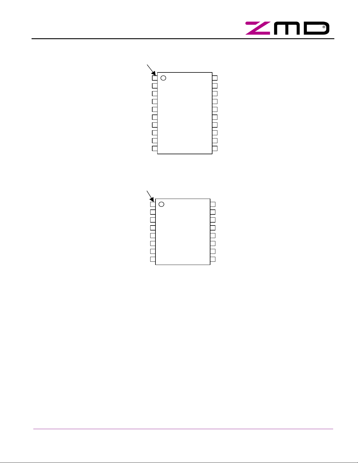
DSTBn
LED1
OSC2
OSC1
P1
P0
D1
D0
P2
P3
D2
D3
PSTBn
LED2
PFAULT
UOUT
U5R
LTGN
CDC
LTGP
Pin 1
DSTBn
LED1
OSC2
OSC1
D1D0D2
D3
PSTBn
LED2
PFAULT
UOUT
U5R
LTGN
LTGP
Pin1
Datasheet
ZENTRUM MIKROELEKTRONIK DRESDEN AG
SAP5S / SAP51
SAP5
Figure 1: SAP5 Package Pin Assignment for the 20 pin version
SAP5
Figure 2: SAP5 Package Pin Assignment for the 16 pin version
CDC
Rev. 2.0, Copyright © 2007, ZMD AG
All rights reserved. The material contained herein may not be reproduced, adapted, merged, translated, stored, or used without the prior written consent of the copyright owner. The
Information furnished in this publication is preliminary and subject to changes without notice.
9/58
Datasheet
ZENTRUM MIKROELEKTRONIK DRESDEN AG
SAP5S / SAP51
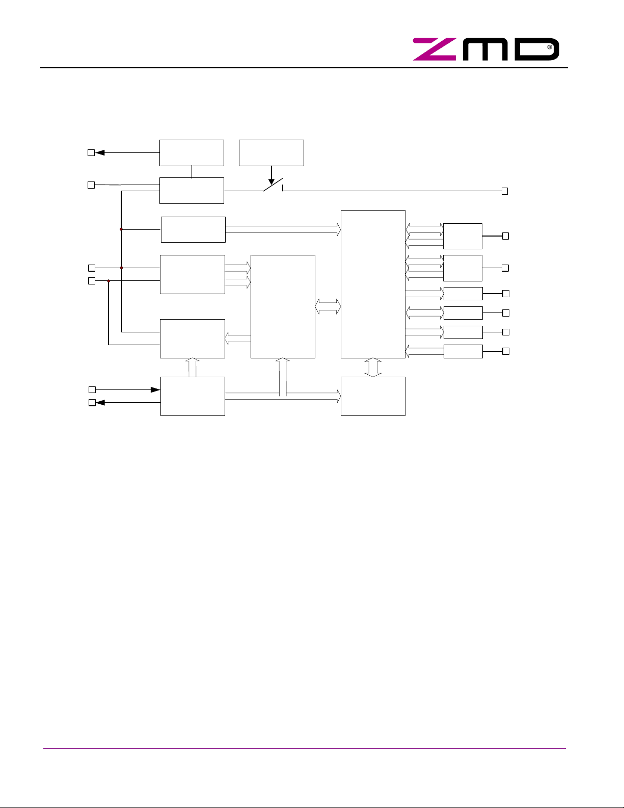
2 Basic Functional Description
2.1 Functional Block Diagram
U5R
CDC
LTGP
LTGN
OSC1
OSC2
Power
Supply
Electronic
Inductor
Power
Fail Detector
Receiver
Transmitter
c
l
k
OSCILLATOR
PLL
Thermal
Protection
APF
pos
neg
MAN
clk
UART
c
l
k
Main
State
Machine
EEPROM
Figure 3: Functional Block Diagram
Param
Offset
Data
Offset
LED
DSTB
PSTB
PFAULT
UOUT
I / O
I / O
Output LED2, LED1
I / O DSTBn
Output PSTBn
Input PFAULT
P3 ... P0
D3 ... D0
Following device functions are associated with the different blocks of the IC:
RECEIVER
The receive block converts the analog telegram waveform from the AS-i bus to a digital
pulse coded signal that can be processed further by a digital UART circuit.
The RECEIVE block is directly connected to the AS-i line pins LTGP and LTGN. It converts
the differential AS-i telegram to a single ended signal and removes the DC offset by high
pass filtering. To adapt quickly on changing signal amplitudes in telegrams from different
network users, the amplitude of the first telegram pulse is measured by a 3 bit flash ADC
and the threshold of a positive and a negative comparator is set accordingly to about 50% of
the measured level. The comparators generate the P-Pulse and N-Pulse signals.
TRANSMITTER
The transmit block transforms a digital response signal to a correctly shaped send current
signal which is applied to the AS-i bus. Due to the inductive network behavior of the network
the changing send current induces voltage pulses on the network line that overlay the DC
operating voltage. The voltage pulses shall have sin²-wave shapes. Hence, the send current
shape must follow the integral of the sin²-wave function.
Rev. 2.0, Copyright © 2007, ZMD AG
All rights reserved. The material contained herein may not be reproduced, adapted, merged, translated, stored, or used without the prior written consent of the copyright owner. The
Information furnished in this publication is preliminary and subject to changes without notice.
10/58

Datasheet
UART /
MAIN STATE
MACHINE /
EEPROM
ELECTRONIC
INDUCTOR
POWER
SUPPLY
OSCILLATOR /
PLL
THERMAL
PROTECTION
POWER FAIL
DETECTOR
INPUT STAGE
OUTPUT
STAGE
ZENTRUM MIKROELEKTRONIK DRESDEN AG
SAP5S / SAP51
E²PROM write access and other I/O operations of the Main State Machine are supported in
Slave Mode only (see description of general IC operational modes below). In Master Mode
the IC is basically equivalent to a physical layer transceiver.
If Slave Mode is activated, the UART demodulates the received telegrams, verifies telegram
syntax and timing and controls a register interface to the Main State Machine. After reception of a correct telegram, the UART generates appropriate Receive Strobe signals, that tell
the Main State Machine to start further processing. The Main State Machine decodes the
telegram information and starts respective I/O processes or E²PROM access. A second
register interface is used to send data back to the UART for construction of a telegram response. The UART modulates the response data into a Manchester-II-coded bit stream that
is used to control the TRANSMITTER unit.
The electronic inductor is basically a gyrator circuit. It provides an inductive behavior between the IC pins LTGP and UOUT while the inductance is controlled by the capacitor on
pin CDC. The inductor decouples the power regulator of the IC as well as the external load
circuit from the AS-i bus and hence prevent cross talk or switching noise from disturbing the
telegram communication on the bus.
The AS-i Complete Specification describes the input impedance behavior of a slave module
by an equivalent circuit that consists of R, L and C in parallel. For example, a slave module
in Extended Address Mode shall have R > 13.5 kOhm, L > 13.5 mH and C < 50pF. The
electronic inductor of the SAP5 delivers values that are well within the required ranges for
output currents up to 55mA (Uin>24V). More detailed parameters can be found in chapter
4.1.
The electronic inductor requires an external capacitor of 10µF at pin UOUT for stability.
The power supply block consists of a bandgap referenced 5V-regulator as well as other
reverence voltage and bias current generators for internal use. The 5V regulator requires an
external capacitor at pin U5R of at least 100nF for stability. It can source up to 4mA for external use, however the power dissipation and the resulting device heating become a major
concern, if too much current is drawn from the regulator. See chapter 4.1.
The oscillator supports direct connection of 5.33 MHz or 16.000 MHz crystals with a dedicated load capacity of 12pF and parasitic pin capacities of up to 8pF. The IC automatically
detects the oscillation frequency of the connected crystal and controls the internal clock
generator circuit accordingly.
After power-on reset the IC is set to 16.000 MHz operation by default. After about 200µs it
will either switch to 5.333 MHz operation or remain in the 16.000 MHz mode. The frequency
detection is active until the first AS-i telegram was successfully received in order to make
sure the IC found the correct clock frequency setting. The detection result is locked thereafter to increase resistance against burst or other interferences.
The oscillator unit also contains a clock watch dog circuit that can generate an unconditioned IC reset if there was no clock oscillation for more than about 20µs. This is to prevent
the IC from unpredicted behavior if no clock signal is available anymore.
The IC is self protected against thermal overload. If the silicon die temperature rises above
around 140°C for more than 2 seconds, the IC detects thermal overheating, switches off the
electronic inductor, performs an IC reset and sets all analog blocks to power down mode.
The 5V-regulator is of course also turned off in this state, however, there will still remain a
voltage of about 3 … 3.5V available at U5R that is derived from the internal start circuitry. If
the overheat condition is left the IC resumes operation and performs an initialization.
The Power Fail Detector observes the voltage at the AS-i-line. It signals at pin PSTBn/APF
when the voltage drops below about 22.5V. Active in Master Mode only.
All digital inputs, except of the oscillator pins, have high voltage capabilities and pull-up
features. For more details see chapters 1.7, 4.3, 4.7, and 4.8.
All digital output stages, except of the oscillator pins, have high voltage capabilities and are
implemented as NMOS open drain buffers. Each pin can sink up to 10mA of current. See
chapter 4.4.
Rev. 2.0, Copyright © 2007, ZMD AG
All rights reserved. The material contained herein may not be reproduced, adapted, merged, translated, stored, or used without the prior written consent of the copyright owner. The
Information furnished in this publication is preliminary and subject to changes without notice.
11/58
ASI+
-
Datasheet
ZENTRUM MIKROELEKTRONIK DRESDEN AG
SAP5S / SAP51
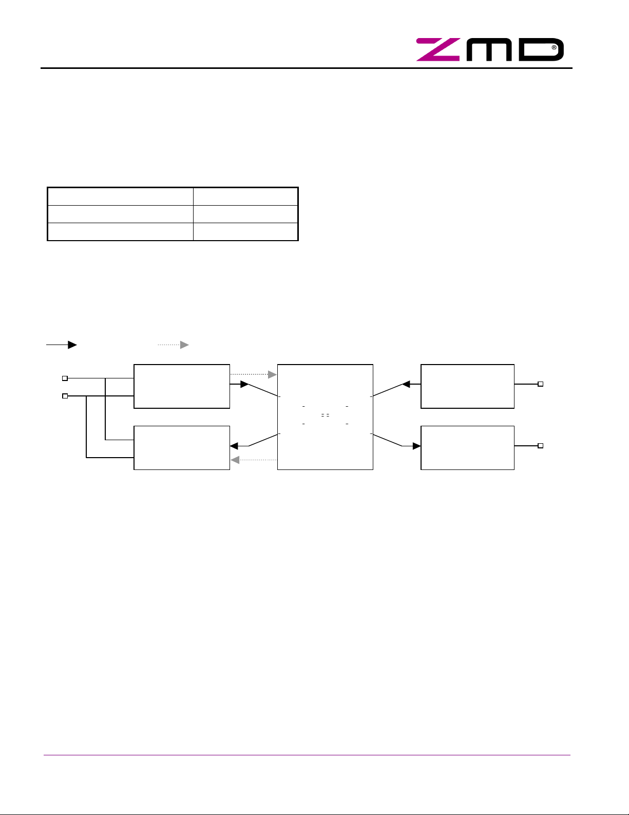
2.2 General Operational Modes
The SAP5 provides two operational modes: Slave Mode and Master/Repeater Mode. A definition of which operational mode becomes active is made by programming the flag Master_Mode in the Firmware Area of the
E²PROM (see also Table 9 on page 19). The E²PROM is read out at every initialization of the IC. Online mode
switching is not provided. The following configurations apply:
Table 5: Assignment of operational modes
Selected Operational Mode Master Mode Flag
Slave Mode 0
Master/Repeater Mode 1
In Slave Mode the SAP5 operates as fully featured AS-i Slave IC according to AS-i Complete Specification v3.0.
In Master/Repeater Mode the SAP5 it acts as physical layer transceiver. It translates a digital output signal from
the master control logic (etc. PLC, µP, …) to a correctly shaped, analog AS-i pulse sequence and vice versa.
Every AS-i telegram received is checked for consistency with the AS-i communication protocol specifications
and if no errors were found, an appropriate receive strobe signal is generated.
The following figure shows the different data path configurations.
Master Mode Slave Mode, ASI-Channel
ASI
ASI- Receiver
UART
ASI- Transmitter
Figure 4: Data path in Master-, Repeater- and Monitor-Mode
More detailed signal descriptions can be found in chapters 4.19 Master- and Repeater Mode as well as 4.14
UART.
CMOS Input
LED Output
D0
(TX)
LED1
(RX)
2.3 Slave Mode
The Slave Mode is the most complex operational mode of the IC. The SAP5 does not only support all mandatory AS-i Slave functions but also a variety of additional features that eases the design of AS-i Slave modules.
2.3.1 AS-i communication channel
The AS-i channel is directly connected to AS-i Bus via the pins LTGP and LTGN. A receiver and a transmitter
unit are connected in parallel to the pins that allow fully bi-directional communication through LTGP and LTGN.
2.3.2 Parameter Port Pins
In the 20-pin package the SAP5 features a 4-bit wide parameter port and a related parameter strobe signal pin
PSTBn. AS-i Complete Specification V3.0 newly defines a bidirectional mode for parameter data. The SAP5
supports this feature, that can be activated by special E²PROM setting (IO_Code, see chapter 4.9).
There is a defined phase relation between a parameter output event, the parameter input sampling and the activation of the PSTBn signal. Thus it can be used to trigger external logic or a micro controller to process the received parameter data or to provide new input data for the AS-i slave response.
Rev. 2.0, Copyright © 2007, ZMD AG
All rights reserved. The material contained herein may not be reproduced, adapted, merged, translated, stored, or used without the prior written consent of the copyright owner. The
Information furnished in this publication is preliminary and subject to changes without notice.
12/58

Datasheet
ZENTRUM MIKROELEKTRONIK DRESDEN AG
SAP5S / SAP51
See chapter 4.7 for further details.
2.3.3 Data Port Pins
The SAP5 provides a 4-bit wide data port. The outputs work independently from each other allowing a maximum
of 4 output devices to be connected to the SAP5. The direction of the Data Port pins are set through the
IO_Code, see chapter 4.9.
The data port is accompanied by the data strobe signal DSTBn. There is a defined phase relation between a
data output event, the input data sampling and the activation of the DSTBn signal. Thus, it can be used to trigger external logic or a micro controller to process the received data or to provide new input data for the AS-i
slave response. See chapter 4.8 for further details.
2.3.4 Data Input Inversion
By default the logic signal (HIGH / LOW) that is present at the data input pins during the input sampling phase is
transferred without modification to the send register, which is interfaced by the UART. By that, the signal becomes directly part of the slave response.
Some applications work with inverted logic levels. To avoid additional external inverters, the input signal can be
inverted by the SAP5 before transferring it to the send register. The inversion of the input signals can be done
jointly for all data input pins. See chapter 4.8.
2.3.5 Data Input Filtering
To prevent input signal bouncing from being transferred to the AS-i Master, the data input signals can be digitally filtered. Activation of the filter is done jointly either by E²PROM configuration or by the logic state of parameter port pin P2. For more detailed information refer to chapter 4.8.
2.3.6 Synchronous Data I/O Mode
AS-i Complete Specification V3.0 newly defines a synchronous data I/O feature, that allows a number of slaves
in the network to switch their outputs at the same time and to have their inputs sampled simultaneously. This
feature is especially useful if more than 4-bit wide data is to be provided synchronously to an application.
The synchronization point was defined to the data exchange event of the slave with the lowest address in the
network. This definition relies on the cyclical slave polling with increasing slave addresses per cycle that is one
of the basic communication principles of AS-i. The IC always monitors the data communication and detects the
change from a higher to a lower slave address. If such a change was recognized, the IC assumes that the slave
with the lower address has the lowest address in the network.
There are some special procedures that become active during the start of synchronous I/O mode operation and
if more than three consecutive telegrams were sent to the same slave address. This is described in more detail
in chapter 4.8.3.
2.3.7 4 Input / 4 Output processing in Extended Address Mode
A new feature of AS-i Complete Specification v3.0 is also support of 4-bit wide output data in Extended Address
Mode. In Extended Address Mode it was, up to Complete Specification v2.11, only possible to send three data
output bits from the master to the slave because telegram bit I3 is used to select between A- and B- slave type
for extended slave addressing (up to 62 slaves per network). In normal address mode I3 carries output data for
pin D3.
The new definition introduces a multiplexed data transfer, so that all 4-bits of the data output port can be used
again. A first AS-i cycle transfers the data for a 2-bit output nibble only, while the second AS-i cycle transfers the
data for the contrary 2-bit nibble. Nibble selection is done by the remaining third bit. To ensure continuous alternation of bit information I2 and thus continued data transfer to both nibbles, a special watchdog was implemented that observes the state of I2 bit. The watchdog can be activated or deactivated by E²RPOM setting. It
provides a watchdog filter time of about 327ms.
The multiplexed transfer of course increases the refresh time per output by a factor of two, however, some applications can tolerate this increase for the benefit of less external circuitry and better slave address efficiency.
The sampling cycle of the data inputs remains unchanged since the meaning of I3 bit was not changed in the
slave response with the definition of the Extended Address Mode.
Rev. 2.0, Copyright © 2007, ZMD AG
All rights reserved. The material contained herein may not be reproduced, adapted, merged, translated, stored, or used without the prior written consent of the copyright owner. The
Information furnished in this publication is preliminary and subject to changes without notice.
13/58

Datasheet
ZENTRUM MIKROELEKTRONIK DRESDEN AG
SAP5S / SAP51
More detailed information is described in chapter 4.8.4.
2.3.8 AS-i Safety Mode
Using the SAP5 Safety Mode makes it easy to implement a safety-related AS-i slave according to the AS-i
Safety at Work concept. Slaves complying with the control category 4 according to EN 954 –1 can be implemented even with a minimum of external circuitry.
In Safety Mode the respond of the SAP5 IC on a Data_Exchange master call (DEXG) is different. Instead of
responding the regular input data provided at the data ports, a 4-bit data word from a specific 8*4 bit code table
is transmitted to the master. Cycling the code table is used to transmit another data word with each DEXG master call. The data transmission is supervised by a Safety Monitor.
In Safety Mode the use of the enhanced data input features described above is disabled. In this case the safety
mode related inputs act as 3-level inputs. See chapter 4.18 for further details.
2.3.9 Enhanced LED Status Indication
The SAP5 IC supports status indication by two LED outputs. More detailed information on the signaling scheme
can be found in chapter 4.11.
2.3.10 Communication Monitor/Watchdog
Data and Parameter communication are continuously observed by a communication monitor. If neither
Data_Exchange nor Write_Parameter calls were addressed to and received by the IC within a time frame of
about 41ms, a so called No Data/Parameter Exchange status is detected and signaled at LED1.
If the respective flags are set in the E²PROM the communication monitor can also act as communication watchdog, that initiates a complete IC reset after expiring of the watchdog timer. The watchdog mode can also be
activated and deactivated by a signal at parameter port pin P0. For more detailed information see chapter 4.17.
2.3.11 Write protection of ID_Code_Extension_1
As defined in AS-i Complete Specification v3.0 the SAP5 also supports write protection for ID_Code_Extension_1. The feature allows the activation of new manufacturer protected slave profiles and is enabled by
E²PROM setting. It is described in more detail in chapter 4.20.
2.3.12 Summary of Master Calls
In Table 6 and Table 7 on the following pages show the complete set of master calls that are decoded by the
SAP5 in Slave Mode. The master calls in Table 7 are intended for programming of the IC by the slave manufacturer only. They become deactivated as soon as the Lock_EE_PRG and Safety_Program_Mode_Disable flag
are set in the Firmware Area of the E²PROM.
AS-i Complete Specification compliance note:
In order to achieve full compliance to the AS-i Complete Specification, the Program_Mode_Disable flag must be
set by the manufacturer of AS-i slave modules during the final manufacturing and configuration process and
before an AS-i slave device is delivered to field application users.
Rev. 2.0, Copyright © 2007, ZMD AG
All rights reserved. The material contained herein may not be reproduced, adapted, merged, translated, stored, or used without the prior written consent of the copyright owner. The
Information furnished in this publication is preliminary and subject to changes without notice.
14/58
Code_1
1
Configuration
0
0
0
0
1
Datasheet
ZENTRUM MIKROELEKTRONIK DRESDEN AG
SAP5S / SAP51
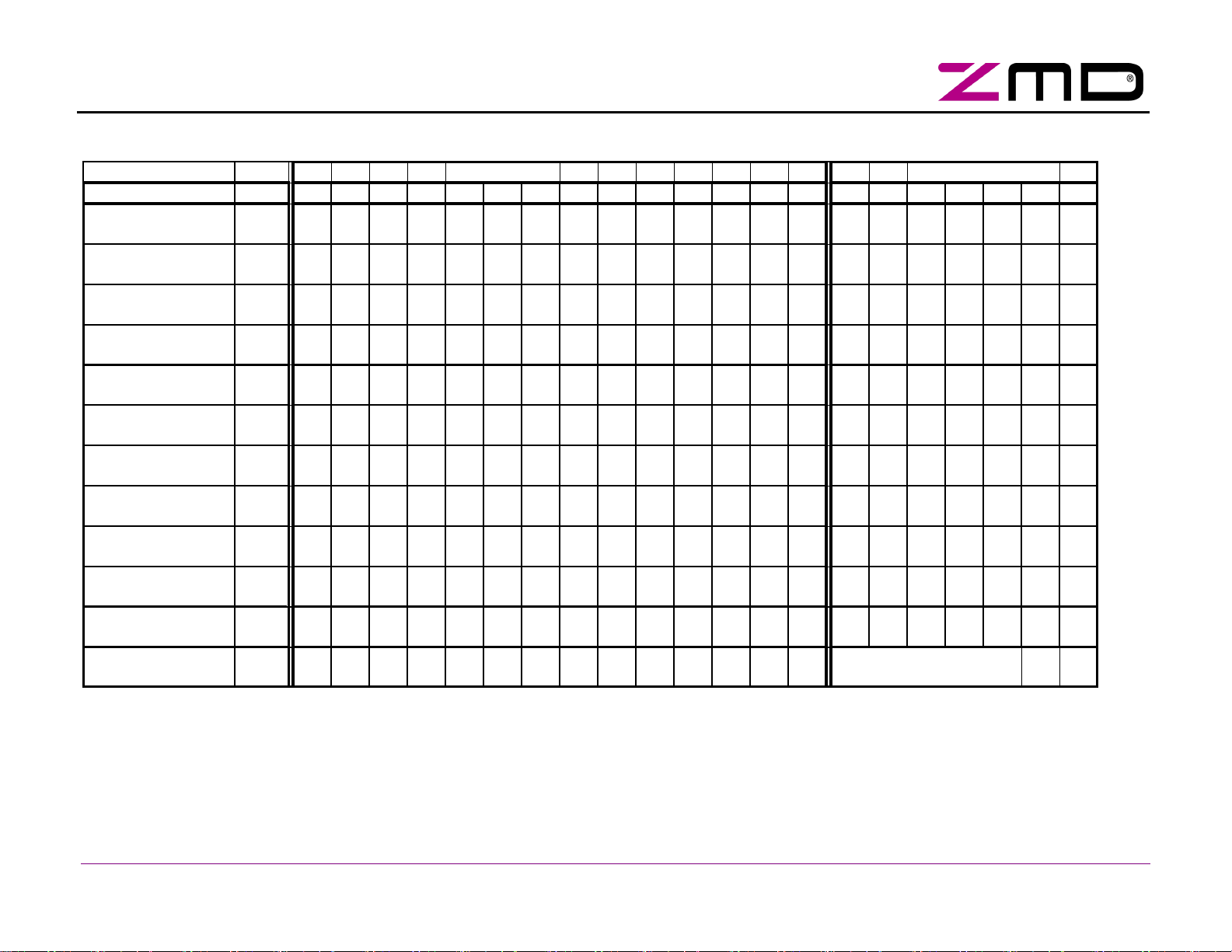
Table 6: SAP5 Master Calls and Related Slave Responses
Master Request Slave Response
Instruction MNE ST CB A4 A3 A2 A1 A0 I4 I3 I2 I1 I0 PB EB SB I3 I2 I1 I0 PB EB
Data Exchange
Write Parameter
DEXG 0 0 A4 A3 A2 A1 A0 0
WPAR 0 0 A4 A3 A2 A1 A0 1
D3
D2 D1 D0 PB 1 0 D3 D2 D1 D0 PB 1
~Sel
P3
P2 P1 P0 PB 1 0 P3 P2 P1 P0 PB 1
~Sel
Address Assignment
Write Extented ID
Delete Address
Reset Slave
Read IO
Read ID Code
Read ID Code_1
Read ID Code_2
Read Status
Broadcast (Reset)
ADRA 0 0 0 0 0 0 0 A4 A3 A2 A1 A0 PB 1 0 0 1 1 0 0 1
WID1 0 1 0 0 0 0 0 0 ID3 ID2 ID1 ID0 PB 1 0 0 0 0 0 0 1
DELA 0 1 A4 A3 A2 A1 A0 0 0 Sel 0 0 0 PB 1 0 0 0 0 0 0 1
RES 0 1 A4 A3 A2 A1 A0 1
RDIO 0 1 A4 A3 A2 A1 A0 1
RDID 0 1 A4 A3 A2 A1 A0 1
RID1 0 1 A4 A3 A2 A1 A0 1
RID2 0 1 A4 A3 A2 A1 A0 1
RDST 0 1 A4 A3 A2 A1 A0 1
~Sel
~Sel
1 0 0 PB 1 0 0 1 1 0 0 1
0 0 0 PB 1 0 IO3 IO2 IO1 IO0 PB 1
Sel
0 0 1 PB 1 0 ID3 ID2 ID1 ID0 PB 1
Sel
0 1 0 PB 1 0 ID3 ID2 ID1 ID0 PB 1
Sel
0 1 1 PB 1 0 ID3 ID2 ID1 ID0 PB 1
Sel
1 1 0 PB 1 0 S3 S2 S1 S0 PB 1
BR01 0 1 1 1 1 1 1 1 0 1 0 1 1 1 --- no slave response ---
NOTE: In extended address mode the "Select Bit" defines whether the A-Slave or B-Slave is being addressed. Dependent on the type of master call the I3 bit carries
the select bit information (Sel) or the inverted select bit information (~Sel). The extended address mode can
Lock_EE_PRG
is at logic LOW level. Refer to chapter 3.3 on page 20 for programming the
Lock_EE_PRG
flag.
not
be activated, as long as the E²PROM flag
Rev 2.0, Copyright © 2007, ZMD AG
All rights reserved. The material contained herein may not be reproduced, adapted, merged, translated, stored, or used without the prior written consent of the copyright owner. The Information furnished in this publication is preliminary and subject to changes without notice.
15/58
Enter Program Mode
Datasheet
ZENTRUM MIKROELEKTRONIK DRESDEN AG
SAP5S / SAP51
Table 7: SAP5 Additional Master Calls for Slave Configuration
Master Request Slave Response
Instruction MNE ST CB A4 A3 A2 A1 A0 I4 I3 I2 I1 I0 PB EB SB I3 I2 I1 I0 PB EB
Set ID Code
Set IO Config
Set ID Code 2
Set Control Code
Set Control Code 2
Safety
(RDIO) 0 1 A4 A3 A2 A1 A0 1 1 0 0 0 PB 1 0 0 1 1 0 0 1
(RDID) 0 1 A4 A3 A2 A1 A0 1 1 0 0 1 PB 1 0 0 1 1 0 0 1
(RID1) 0 1 A4 A3 A2 A1 A0 1 1 0 1 0 PB 1 0 0 1 1 0 0 1
(RID2) 0 1 A4 A3 A2 A1 A0 1 1 0 1 1 PB 1 0 0 1 1 0 0 1
(RES) 0 1 A4 A3 A2 A1 A0 1 0 1 0 0 PB 1 0 0 1 1 0 0 1
PRGM 0 1 0 0 0 0 0 1 1 1 0 1 1 1 --- no slave response ---
Rev. 2.0 Copyright © 2007, ZMD AG
All rights reserved. The material contained herein may not be reproduced, adapted, merged, translated, stored, or used without the prior written consent of the copyright owner. The Information furnished in this publication is preliminary and subject to changes without notice.
16/58

Datasheet
ZENTRUM MIKROELEKTRONIK DRESDEN AG
SAP5S / SAP51
3 E²PROM
3.1 Overview
The SAP5 provides an on-chip E²PROM with typical write and read times according to Table 8.
Table 8: E²PROM Read and Write Times
Symbol Parameter Min Max. Unit Note
t
Initialization readout time 50.0
read_init
t
wrt_adra1
t
wrt_adra2
t
wrt_wid1u
Write time after ADRA master request
Write time after ADRA master request
Write time after WID1 master request
38.0 ms
12.5 ms
38.0 ms
s
µ
(user access)
t
wrt_wid1m
Write time after WID1 master request
25.0 ms
(manufacturer access)
t
1
Single cell write time 12.5 ms
wrt_prgm
Time includes readout of the configuration block. Running in Safety Mode, the User/Firmware Area and the
Safety Area will be read out in parallel.
2
the Lock_EE_PRG flag is set
3
the Lock_EE_PRG flag is not yet set
4
concerns the programming of data in both Firmware Area and Safety Area
For security reasons the memory area is structured in three independent data blocks and a single configuration
block containing the Security_Flag. The data blocks are named User Area, Firmware Area and Safety Area.
The Firmware Area contains all manufacturing related configuration data (i.e. selection of optional features, ID
codes, …). It can be protected against undesired data modification by setting the Lock_EE_PRG flag to ‘1’.
The User Area contains only such data that is relevant for changes at the final application (i.e. field installation
of slave module). Because the environment where modifications of the user data may become necessary can
sometimes be rough and unpredictable, additional security was added to the programming of the User Area,
ensuring a write access cannot result in an undetected corruption of E²PROM data.
The Safety Area contains the cryptographic code table for the Safety Mode.
The E²PROM cells in User Area, Firmware Area and Safety Area have a word width of 6 bit. The sixth bit is not
shown in Table 9 and Table 11. The sixth bit of each cell represents the odd parity of the respective data word,
providing an additional data security mechanism. The programming of the parity bit is performed automatically
during the E²PROM write process and cannot be influenced by the user. Each E²PROM read process – particularly during initialization of the SAP5 – involves an evaluation of the parity bits. In case a wrong parity bit was
found in the User Area, the entire User Area data is treated as corrupted. The IC returns to Slave Address “0”
and the ID_Code as well as the IO_Code are set to 0xF. In case a false parity bit was found in one or more cells
of the Firmware Area or the Safety Area, the status register bit S1 will be set (=’1’), signaling the same state as
the input PFAULT would be set (refer to chapter 4.16 page 40).
1
2
3
2
3
4
3.2 User Area Programming
User Area data can be written by an ADRA or WID1 master request (refer to Table 6). Any such write access is
accompanied by two write steps to the Security_Flag, one before and one after the actual modification of user
data.
The following procedure is executed when writing to the User Area of the E²PROM:
1. The Security_Flag is programmed to ‘1’.
2. The content of the Security_Flag is read back, verifying it was programmed to ‘1’.
3. The user data is modified.
Rev. 2.0, Copyright © 2007, ZMD AG
All rights reserved. The material contained herein may not be reproduced, adapted, merged, translated, stored, or used without the prior written consent of the copyright owner. The
Information furnished in this publication is preliminary and subject to changes without notice.
17/58

Datasheet
ZENTRUM MIKROELEKTRONIK DRESDEN AG
SAP5S / SAP51
4. A read back of the written data is performed.
5. If the read back has proven successful programming of the user data, the Security_Flag
is programmed back to ‘0’.
6. The content of the Security_Flag is read back, verifying it was programmed to ‘0’.
Successful execution of the E²PROM write procedure may be observed at the status register contents. If bit S0
is set (logic HIGH) the write process is not finished yet and the programming data is still volatile. If bit S3 (equals
the Security_Flag) is set, the write procedure did not successfully complete either because the write cycle was
interrupted or due to an internal error. In order to program the data correctly the write request should be repeated. The status register can be read using the AS-i Master call Read_Status (RDST).
In addition to a read out of the data areas, the Security_Flag of the E²PROM is also read and evaluated during
IC initialization. In case the value of the Security_Flag equals ‘1’ (i.e. due to an undesired interruption of a User
Area write access), the entire User Area data is treated as corrupted. The IC returns to Slave Address “0” and
the ID_Code as well as the IO_Code are set to 0xF. Consequently, the programming of the User Area data can
be repeated.
Rev. 2. 0, Copyright © 2007, ZMD AG
All rights reserved. The material contained herein may not be reproduced, adapted, merged, translated, stored, or used without the prior written consent of the copyright owner. The
Information furnished in this publication is preliminary and subject to changes without notice.
18/58
 Loading...