

ZMD ASI4U Datasheet
ASI4U
ASIP
ASIN
0V
IRD
FID
OSC1
OSC2
DO3
DO2
DO1
DO0
GND
P3
P2
UIN
UOUT
U5R
CAP
LED1
LED2
DSR
PST
DI3
DI2
DI1
DI0
P0
P1
1µF
10µF
47nF
ASI+
ASI-
8/16 MHz
IR Addressing
nel
Universal Actuator-Sensor Interface IC
Datasheet
Features
Universal application in AS-i Slave, Mas-
•
ter, Repeater and Bus-Monitor components
Support of AS-i Complete Specification
•
V3.0, including all optional features
-
Synchronous Data I/O Mode
4 Input / 4 Output operation in
-
Extended Address Mode
User write protection for
-
Extended ID-Code 1
Multiplexed Parameter Port
-
Special AS-i Safety Mode
•
Floating AS-i Transmitter and Receiver for
•
high symmetrical high power applications
On chip electronic inductor with current
•
drive capability of 55mA
Configurable LED outputs supporting all
•
status indication modes defined by AS-i
Complete Specification V3.0
Several data preprocessing functions, in-
•
cluding configurable data input filters and
bit selective data inverting
Improved additional addressing channel
•
for easy module setup
IR and CMOS input mode
-
Activation by magic sequence
-
Support of 8 / 16 MHz crystals by auto-
•
matic frequency detection
Clock Watchdog for high System Security
•
Pin and function compatible to A²SI
•
Description
ASI4U is a monolithic CMOS integrated circuit
certified for AS-i (Actuator Sensor Interface)
networks. AS-i networks are used for industrial
automation.
AS-i is designed for easy and simple interconnection of binary sensors and actuators. It
uses a two-wire unshielded cable to transport
power and information.
ASI4U is a direct successor of the A²SI IC and
can replace the A²SI.
AS-i Safety applications can use the special
AS-i Safety Mode if fault reaction time is a
concern.
The device is available in SSOP28 package.
Application Support
Configuration of the chip is handled through
programming of the on-chip E²PROM.
ZMD provides a special
AS-Interface Programmer Tool
(Ordering Code: ZMD ASI-Programmer )
to ease product evaluation and selection of
different operation modes.
Further application support is available through
the e-mail hotline asi@zmd.de
BZV55C39
Chan
Copyright © 2006, ZMD AG, Rev. 1.5
All rights reserved. T he material contained herein may not be reprod uced, adapted, merged, translated, stored, or used without the pri or written co nsent of the co pyright owner. The
Information furnished in this publication is preliminary and subject to changes without notice.
TEMD5000
1/57

Datasheet
ZENTRUM MIKROELEKTRONIK DRESDEN AG
“ASI for you” IC
Table of Contents
0 READ THIS FIRST ...........................................................................................................................................4
0.1 I
0.2 ASI-S
0.3 R
1 GENERAL DEVICE SPECIFICATION.............................................................................................................5
1.1 A
1.2 O
1.3 Q
1.4 P
2 BASIC FUNCTIONAL DESCRIPTION ............................................................................................................9
2.1 F
2.2 G
2.3 S
2.4 M
2.5 E²PROM ..................................................................................................................................................18
3 DETAILED FUNCTIONAL DESCRIPTION ...................................................................................................21
3.1 AS-I R
3.2 AS-I T
3.3 A
3.4 D
3.5 D
3.6 P
3.7 D
MPORTANT NOTICE
AFETY APPLICATIONS
EPAIR OF
BSOLUTE MAXIMUM RATINGS (NON OPERATING
PERATING CONDITIONS
UALITY STANDARDS
ACKAGE PIN ASSIGNMENT
UNCTIONAL BLOCK DIAGRAM
ENERAL OPERATIONAL MODES
LAVE MODE
2.3.1 AS-i communication channel ...........................................................................................................11
2.3.2 IRD communication channel ............................................................................................................12
2.3.3 Parameter Port Pins.........................................................................................................................12
2.3.4 Data Port Pins ..................................................................................................................................12
2.3.5 Data Input Inversion .........................................................................................................................13
2.3.6 Data Input Filtering...........................................................................................................................13
2.3.7 Fixed Data Output Driving................................................................................................................13
2.3.8 Synchronous Data I/O Mode............................................................................................................13
2.3.9 4 Input / 4 Output processing in Extended Address Mode ..............................................................13
2.3.10 AS-i Safety Mode .............................................................................................................................14
2.3.11 Enhanced LED Status Indication .....................................................................................................14
2.3.12 Communication Monitor/Watchdog ..................................................................................................14
2.3.13 Write protection of ID_Code_Extension_1 .......................................................................................14
2.3.14 Summary of Master Calls.................................................................................................................14
ASTER MODE
DDRESSING CHANNEL INPUT
3.3.1 General Slave Mode Functionality ...................................................................................................22
3.3.2 AC Current Input Mode ....................................................................................................................23
3.3.3 CMOS Input Mode ...........................................................................................................................23
3.3.4 Master-, Repeater- and Monitor-Mode.............................................................................................24
IGITAL INPUTS
IGITAL OUTPUTS
ARAMETER PORT AND
3.6.1 Slave Mode ......................................................................................................................................26
3.6.2 Parameter Multiplex Mode ...............................................................................................................27
3.6.3 Special function of P0, P1 and P2 ...................................................................................................27
3.6.4 Master-, Repeater-, Monitor Mode ...................................................................................................28
ATA PORT AND
3.7.1 Slave Mode ......................................................................................................................................29
3.7.2 Input Data Pre-Processing ...............................................................................................................30
3.7.3 Fixed Output Data Driving................................................................................................................32
3.7.4 Synchronous Data I/O Mode............................................................................................................32
3.7.5 Support of 4I/4O processing in Extended Address Mode, Profile 7.A.x.E .......................................34
3.7.6 Safety Mode Operation ....................................................................................................................34
3.7.7 Master-, Repeater-, Monitor Mode ...................................................................................................38
3.7.8 Special function of DSR ...................................................................................................................38
ASI-S
.............................................................................................................................................11
..........................................................................................................................................17
ECEIVER
RANSMITTER
..........................................................................................................................................21
.....................................................................................................................................4
.........................................................................................................................4
AFETY MODULES
.............................................................................................................................6
..................................................................................................................................6
..........................................................................................................................7
....................................................................................................................................21
- DC C
HARACTERISTICS
- DC C
DSR PIN.........................................................................................................................29
HARACTERISTICS
PST PIN................................................................................................................26
...............................................................................................................4
) ........................................................................................5
......................................................................................................................9
................................................................................................................11
IRD .............................................................................................................22
....................................................................................................25
................................................................................................25
Page
Copyright © 2006, ZMD AG, Rev.1.5
All rights reserved. The material contained herein may not be repr oduced, ad apted, merged, translated, stored, or used without the prior written consent of the copyright o wner. T he
Information furnished in this publication is preliminary and subject to changes without notice.
2/57

Datasheet
3.8 F
3.9 LED
3.10
3.11
3.12
3.13
3.14
3.15
3.16
3.17
3.18
4 APPLICATION CIRCUITS .............................................................................................................................51
5 PACKAGE OUTLINE.....................................................................................................................................54
6 PACKAGE MARKING ...................................................................................................................................55
7 ORDERING INFORMATION..........................................................................................................................55
8 RELATED DOCUMENTS ..............................................................................................................................56
9 RELATED PRODUCTS .................................................................................................................................56
10 CONTACT INFORMATION ........................................................................................................................56
10.1
10.2
10.3
10.4
AULT INDICATION INPUT PIN
3.8.1 Slave Mode ......................................................................................................................................39
3.8.2 Master- and Monitor Mode ...............................................................................................................39
3.9.1 Slave Mode ......................................................................................................................................40
3.9.2 Communication via Addressing Channel.........................................................................................41
3.9.3 Master-, Repeater-, Monitor Mode...................................................................................................41
O
IC R
3.11.1 Power On Reset...............................................................................................................................42
3.11.2 Logic controlled Reset .....................................................................................................................43
3.11.3 External Reset .................................................................................................................................43
UART ...................................................................................................................................................44
3.12.1 AS- i input channel ...........................................................................................................................44
3.12.2 Addressing Channel.........................................................................................................................46
M
C
T
W
P
3.17.1 Voltage Output Pins UOUT and U5R ..............................................................................................49
3.17.2 Input Impedance (AS-i bus load) .....................................................................................................50
T
ZMD S
ZMD AS-I
AS-I
ZMD D
OUTPUTS
SCILLATOR PINS
ESET
AIN STATE MACHINE
OMMUNICATION MONITOR/WATCHDOG
OGGLE WATCHDOG FOR
RITE PROTECTION OF
OWER SUPPLY
HERMAL AND OVERLOAD PROTECTION
NTERNATIONAL ASSOCIATION
...........................................................................................................................................40
..............................................................................................................................................42
.....................................................................................................................................49
ALES
..........................................................................................................................................56
NTERFACE APPLICATION SUPPORT
ISTRIBUTION PARTNERS
ZENTRUM MIKROELEKTRONIK DRESDEN AG
“ASI for you” IC
FID...............................................................................................................39
OSC1, OSC2 ...........................................................................................................41
............................................................................................................................47
.................................................................................................47
4I/4O
PROCESSING IN EXTENDED ADDRESS MODE
ID_C
ODE_EXTENSION
..........................................................................................................56
..............................................................................................................57
_1 ...................................................................................47
..................................................................................................50
..........................................................................................56
...........................................47
Copyright © 2006, ZMD AG, Rev.1.6
All rights reserved. T he material contained herein may not be reprod uced, adap ted, merged, translated, stored, or used without the prior written consent of the copyright owner. T he
Information furnished in this publication is preliminary and subject to changes without notice.
3/57

Datasheet
ZENTRUM MIKROELEKTRONIK DRESDEN AG
“ASI for you” IC
0 Read this First
0.1 Important Notice
Products sold by ZMD are covered exclusively by the warranty, patent indemnification and other provisions appearing in ZMD standard "Terms of Sale". ZMD makes no warranty (express, statutory, implied and/or by description), including without limitation any warranties of merchantability and/or fitness for a particular purpose,
regarding the information set forth in the Materials pertaining to ZMD products, or regarding the freedom of any
products described in the Materials from patent and/or other infringement. ZMD reserves the right to discontinue
production and change specifications and prices of its products at any time and without notice. ZMD products
are intended for use in commercial applications. Applications requiring extended temperature range, unusual
environmental requirements, or high reliability applications, such as military, medical life-support or lifesustaining equipment, are specifically not recommended without additional mutually agreed upon processing by
ZMD for such applications.
ZMD reserves the right to change the detail specifications as may be required to permit improvements in the
design of its products.
0.2 ASI-Safety Applications
SAFETY-ADVICE
The ASI4U is designed to allow replacement of A²SI ICs in existing board layouts and applications. However,
since the ASI4U provides additional data preprocessing functions at the data input channel, the fault reaction
time of an AS-i Safety module could increase by 40ms if some of the new features become activated by intention, by accident or hardware fault.
ZMD strongly recommends the use of the new ASI4U Safety-Mode, if the ASI4U shall replace the A²SI in existing ASI-Safety designs. Only then, the same fault reaction times as with the A²SI are guaranteed. For compatibility with the modified data input routing in Safety Mode, the user has to adapt the safety code table stored in
the external micro controller. Only such Safety Code Sequences that contain the value 1110 are permitted.
If the IC is operated in Safety Mode, the user must pay special attention that the Synchronous Data I/O Mode as
well as the Data Input Filters remain disabled by appropriate E²PROM configuration.
Application of the ASI4U in Standard Mode (no Safety Mode enabled) for AS-i Safety products is basically possible, if an additional Fault Reaction Time of 40ms is taken into account.
The user shall also obey the additional security advice regarding “Production and Repair of AS-i Safety Slaves”
that is available as an additional document form the ZMD web page www.zmd.biz .
0.3 Repair of ASI-Safety Modules
If an A²SI based ASI-Safety Module shall be repaired, it is explicitly prohibited to replace the A²SI IC with the
newer ASI4U IC. This is to exclude safety relevant deviations of module properties that can result from the different data input paths an the above mentioned possible increase in Fault Reaction Time.
The user shall also obey the additional security advice regarding “Production and Repair of AS-i Safety Slaves”
that is available as an additional document form the ZMD web page www.zmd.biz .
Copyright © 2006, ZMD AG, Rev.1.6
All rights reserved. The material contained herein may not be repr oduced, ad apted, merged, translated, stored, or used without the prior written consent of the copyright o wner. T he
Information furnished in this publication is preliminary and subject to changes without notice.
4/57
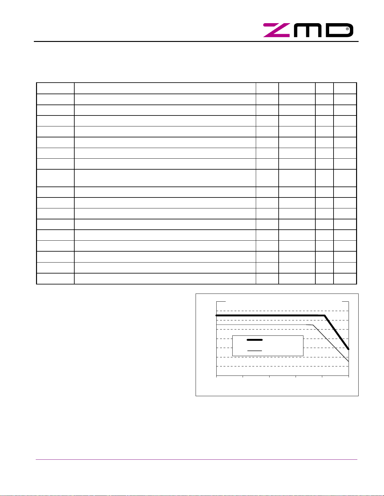
Figure
1
: Ptot = f(
θ
)
Datasheet
ZENTRUM MIKROELEKTRONIK DRESDEN AG
“ASI for you” IC
1 General Device Specification
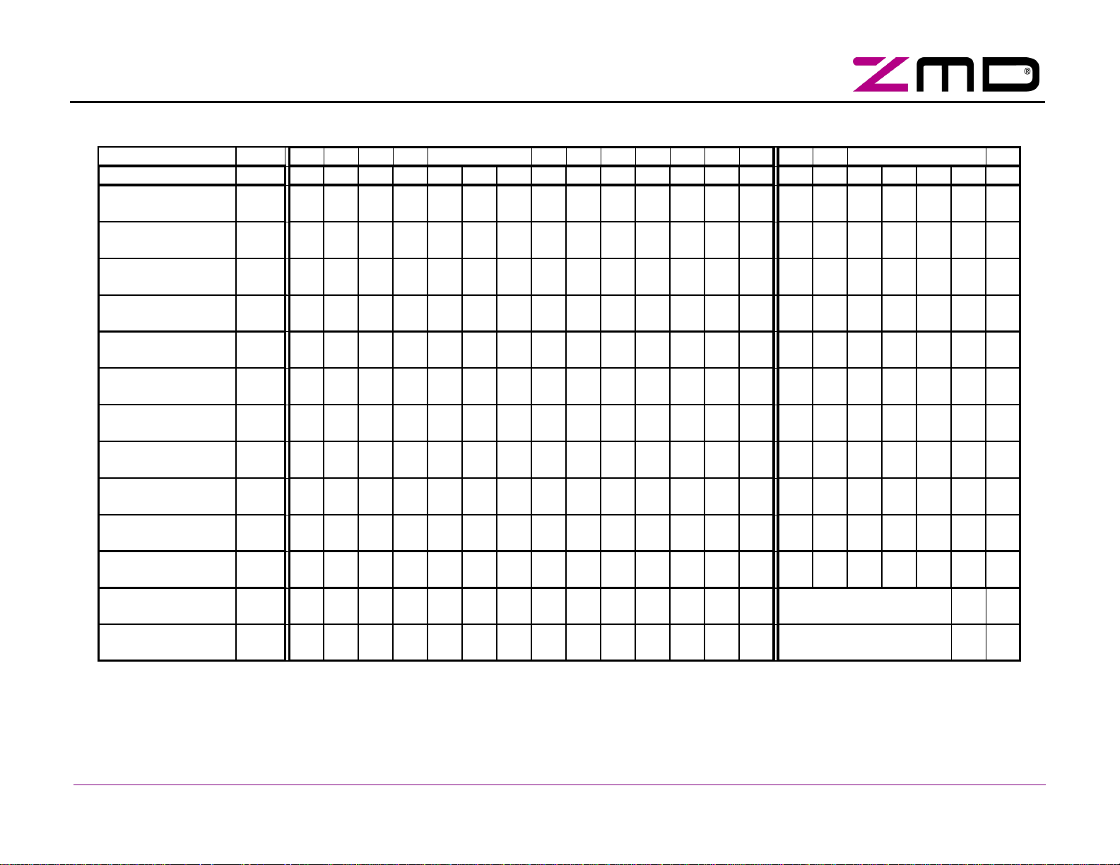
1.1 Absolute Maximum Ratings (Non Operating)
Table 1: Absolute Maximum Ratings
Symbol Parameter Min Max Unit Note
V0V, V
V
ASIP-ASIN
V
ASIP-ASIN_P
V
ASIP
V
ASIN
V
UIN
V
UIN_P
V
inputs1
V
inputs2
Iin Input current into any pin except supply pins -50 50 mA
H Humidity non-condensing
V
HBM1
V
HBM2
V
EDM
θ
STG
P
tot
R
thj
Voltage reference 0 0 V
GND
Voltage difference between ASIP and ASIN (V
Pulse voltage between ASIP and ASIN (V
Pulse voltage between ASIP and 0V (V
Voltage between ASIN and 0V (V
– V0V) -6.0 6.0 V
ASIN
ASIP
– V0V) -0.3 50 V
ASIP
ASIP
- V
- V
ASIN
) -0.3 40 V
ASIN
) -0.3 50 V
Power supply input voltage -0.3 40 V
Pulse voltage at power supply input -0.3 50 V
Voltage at pins DI3 ... DI0, DO3 ... DO0, P3 ... P0, DSR, PST,
-0.3 V
+ 0.3 V
UOUT
LED1, LED2, FID, IRD, UOUT
Voltage at pins OSC1, OSC2, CAP, U5R -0.3 7 V
Electrostatic discharge – Human Body Model (HBM1) 3500 V
Electrostatic discharge – Human Body Model (HBM2) 2000 V
Electrostatic discharge – Equipment Discharge Model (EDM) 400 V
Storage temperature -55 125 °C
Total power dissipation 0.85 W
Thermal resistance of SSOP 28 package 40 80 K/W
1
2
2, 3
3
2
4
5
6
7
8
9
10
1
reverse polarity protection has to be performed
externally
2
pulse with ≤ 50µs, repetition rate ≤ 0.5 Hz
3
V
ASIP-ASIN
4
Latch-up resistance, reference pin is 0V
5
Level 4 according to JEDEC-020A is guaranteed
6
HBM1: C = 100pF charged to V
and V
ASIP-ASIN_P
must not be violated
with resistor
HBM1
R = 1.5kΩ in series, valid for ASIP-ASIN only.
7
HBM2: C = 100pF charged to V
with resistor
HBM2
R = 1.5kΩ in series, valid for all pins except ASIP-
ASIN
8
EDM: C = 200pF charged to V
with no resistor
EDM
in series, valid for ASIP-ASIN only
9
at max. operating temperature, the allowed total
1
0.9
0.8
0.7
0.6
0.5
0.4
0.3
0.2
P
= f (Ta); 1L / 2L = 1 layer / 2 layer PCB
tot
Ptot (2L)
Ptot (1L)
-25 0 25 50 75 100
Ta
power dissipation depends on additional thermal
resistance from package to ambient and on the operation ambient temperature as shown in Figure 1.
10
Single layer board, P
Copyright © 2006, ZMD AG, Rev.1.6
All rights reserved. T he material contained herein may not be reprod uced, adap ted, merged, translated, stored, or used without the prior written consent of the copyright owner. T he
Information furnished in this publication is preliminary and subject to changes without notice.
= 0.5W; air velocity = 0m/s ⇒ max. value; air velocity = 2.5m/s ⇒ min. value
tot
5/57
Datasheet
ZENTRUM MIKROELEKTRONIK DRESDEN AG
“ASI for you” IC
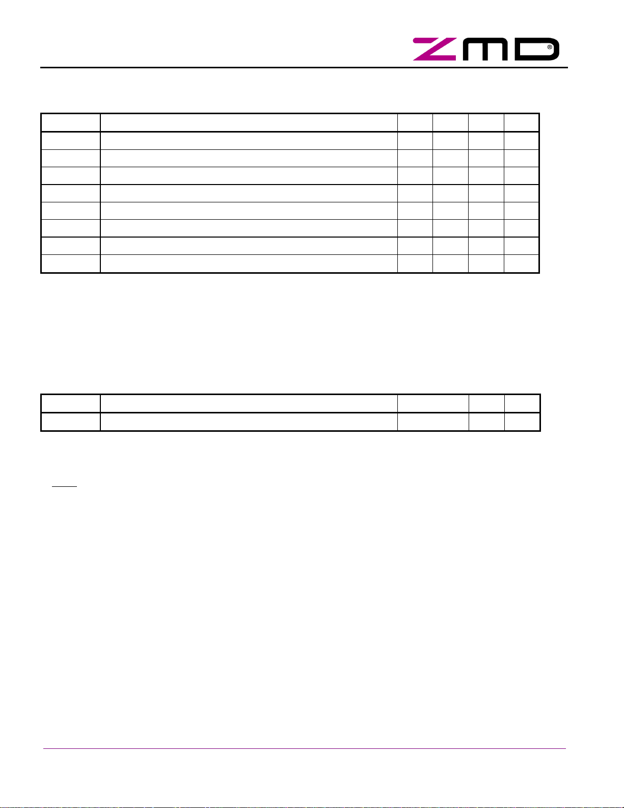
1.2 Operating Conditions
Table 2: Operating Conditions
Symbol Parameter Min Max. Unit Note
V
Positive supply voltage for IC operation 16 33.1 V
UIN
V0V, V
V
ASIP
V
ASIN
I
UIN
I
CL1
I
CL2
θ
amb
1
DC-Parameter: V
V
Below V
Negative supply voltage 0 0 V
GND
DC voltage at ASIP relating to V0V 16 33.1 V
DC voltage at ASIN relating to V0V -4 4 V
Operating current at V
= 30V 6 mA
UIN
Max. output sink current at pins DO3...DO0, DSR 10 mA
Max. output sink current at pins P0...P3, PST 10 mA
Ambient temperature range, operating range -25 85 °C
= V
UINmin
= V
UINmax
the power supply block may not be able to provide the specified output currents at
UINmin
UOUTmin
UOUTmax
+ V
+ V
DROPmax
DROPmin
UOUT and U5R.
2
Outside of these limits the send current shape and send current amplitude cannot be guaranteed.
3
fc = 8.000 MHz, no load at any pin, transmitter turned off, digital state machine is in idle state
Table 3: Crystal Frequency
1
2
2
3
Symbol Parameter Nom. Unit Note
fc Crystal frequency 8.000/16.000 MHz
4
The IC automatically detects whether the crystal frequency is 8.000MHz or 16.000MHz and controls the
4
internal clock circuit accordingly. The frequency detection is locked as soon as one AS-i telegram was
correctly received at any input channel. It can be reset by Power On Reset only.
Note: In Slave Mode the locking occurs if a Master Call was received. In Master-/ Repeater-/Monitor
Mode a Master Call or a Slave Response that was received on any input channel, triggers the frequency
locking.
The ASI4U supports an integrated clock watchdog. If no crystal or clock oscillation is recognized for 150µs the
IC generates a RESET event until clock oscillation is available.
More detailed oscillator pin definitions can be found in chapter 3.10 on page 41.
1.3 Quality Standards
The quality of the IC will be ensured according to the ZMD quality standards. Functional device parameters are
valid for device operating conditions specified in chapter 1.2. Production device tests are performed within the
recommended ranges of V
otherwise stated.
ASIP
- V
, VIN - V0V, θamb = + 25°C (+ 85°C and - 25°C on sample base only) unless
ASIN
Copyright © 2006, ZMD AG, Rev.1.6
All rights reserved. The material contained herein may not be repr oduced, ad apted, merged, translated, stored, or used without the prior written consent of the copyright o wner. T he
Information furnished in this publication is preliminary and subject to changes without notice.
6/57

i Transmitter/Receiver input, to be connected to
d to
Datasheet
ZENTRUM MIKROELEKTRONIK DRESDEN AG
1.4 Package Pin Assignment
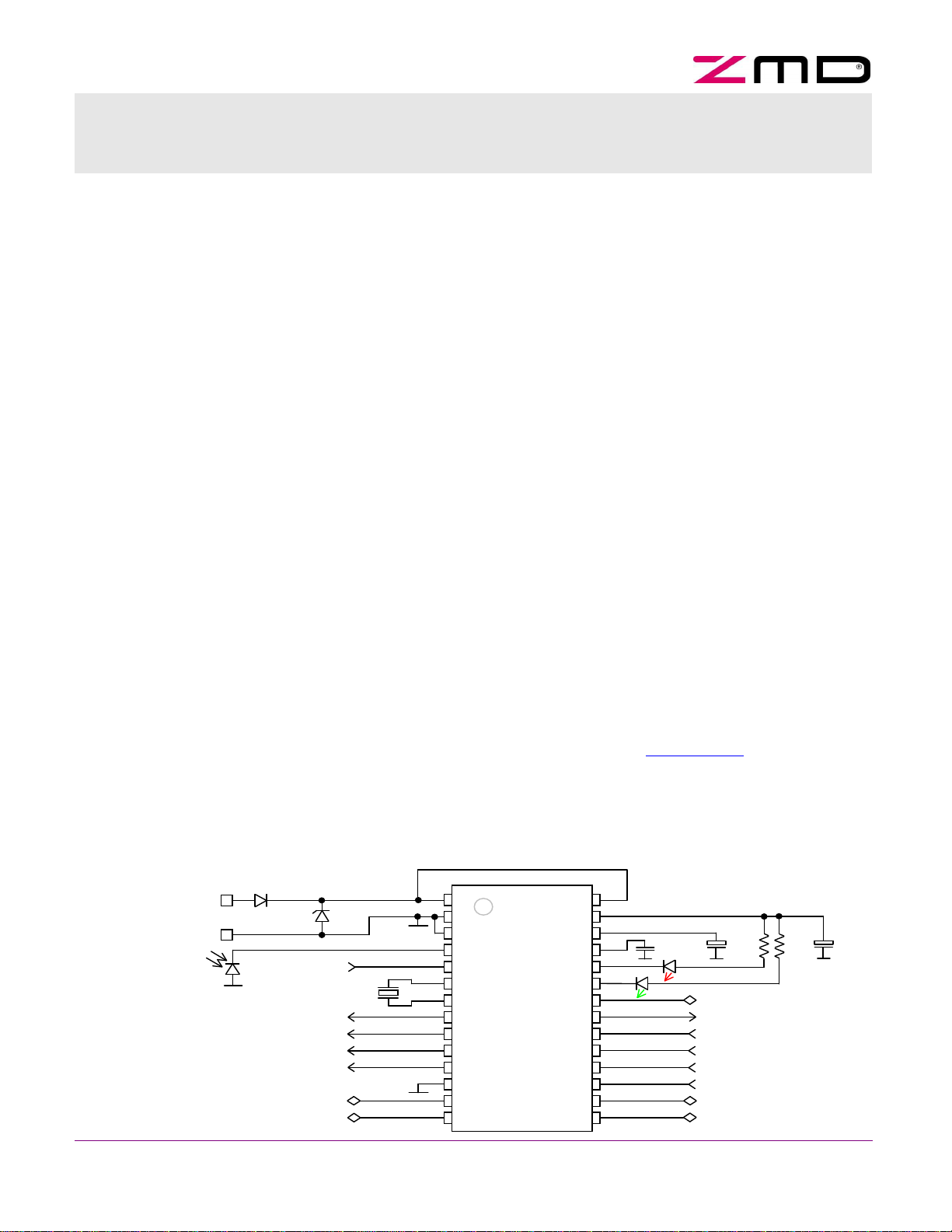
Table 4: ASI4U Pin List
“ASI for you” IC
Package
Name Direction Type Description
pin number
1 ASIP IN Analog AS-
ASI+ lead of AS-i cable, via reverse polarity protection diode
2 ASIN OUT Analog AS-i Transmitter/Receiver output, to be connecte
ASI- lead of AS-i cable
3 0V SUPPLY IC Ground
Common ground for all IC ports except ASIP/ASIN,
To be connected to ASIN if no external coils are used
4 IRD IN Analog / CMOS (5V) Addressing Channel input
5 FID IN Pull-up Periphery Fault input
6 OSC2 OUT Analog (5V) Crystal oscillator
7 OSC1 IN Analog / CMOS (5V) Crystal oscillator / External clock input
8 DO3 OUT Open Drain Data port output D3
9 DO2 OUT Open Drain Data port output D2
10 DO1 OUT Open Drain Data port output D1
11 DO0 OUT Open Drain Data port output D0
12 GND SUPPLY Digital I/O ground, to be connected with 0V
13 P3 I/O Pull-up/Open Drain Parameter port P3
14 P2 I/O Pull-up/Open Drain Parameter port P2 /
Receive Strobe output in Master Mode
15 P1 I/O Pull-up/Open Drain Parameter port P1 /
Power Fail output in Master Mode
16 P0 I/O Pull-up/Open Drain Parameter port P0 /
Data Clock output in Master Mode
17 DI0 IN Pull-up Data port input D0
18 DI1 IN Pull-up Data port input D1
19 DI2 IN Pull-up Data port input D2
20 DI3 IN Pull-up Data port input D3
21 PST I/O Pull-up/Open Drain Parameter Strobe output
(input function used for IC test purposes only)
22 DSR I/O Pull-up/Open Drain Data Strobe output / Reset input
Copyright © 2006, ZMD AG, Rev.1.6
All rights reserved. T he material contained herein may not be reprod uced, adap ted, merged, translated, stored, or used without the prior written consent of the copyright owner. T he
Information furnished in this publication is preliminary and subject to changes without notice.
7/57
LED output "Enhanced Diagnosis", to be activated by
bit in the Firmware region of the
ASIP
ASIN
0V
IRD
FID
OSC2
OSC1
O3
DO2
DO1
DO0
GND
P3
P2
UOUT
LED2
Figure
2
:
Package Pin Assignment
Datasheet
ZENTRUM MIKROELEKTRONIK DRESDEN AG
“ASI for you” IC
Package
Name Direction Type Description
pin number
23 LED2 OUT Open Drain
LED2_Active
E²PROM
24 LED1 I/O Pull-up/Open Drain LED output "AS-i-Diagnosis" /
Addressing channel output
(input function used for IC test purposes only)
25 CAP I/O Analog Filter control (Electronic Inductor)
26 U5R OUT Analog Regulated internal/external 5V supply
27 UOUT OUT Analog Decoupled Actuator/Sensor supply
28 UIN SUPPLY Power supply input
All open drain outputs are NMOS based. Pull-up properties at input stages are achieved by current sources
referring to U5R.
UIN
U5R
CAP
LED1
D
ASI4U
DSR
PST
DI3
DI2
DI1
DI0
P0
P1
Copyright © 2006, ZMD AG, Rev.1.6
All rights reserved. The material contained herein may not be repr oduced, ad apted, merged, translated, stored, or used without the prior written consent of the copyright o wner. T he
Information furnished in this publication is preliminary and subject to changes without notice.
8/57
POWER
SUPPLY
OSCILLATOR
AGND
OUTPUT
STAGE
INPUT
STAGE
I/O
STAGE
OUTPUT
STAGE
INPUT
STAGE
OUTPUT
STAGE
AC
FAULT_IN
ELECTRONIC
INDUCTOR
ANA DIG
FID LED2
LED1
IRD GND 0V
Datasheet
ZENTRUM MIKROELEKTRONIK DRESDEN AG
“ASI for you” IC
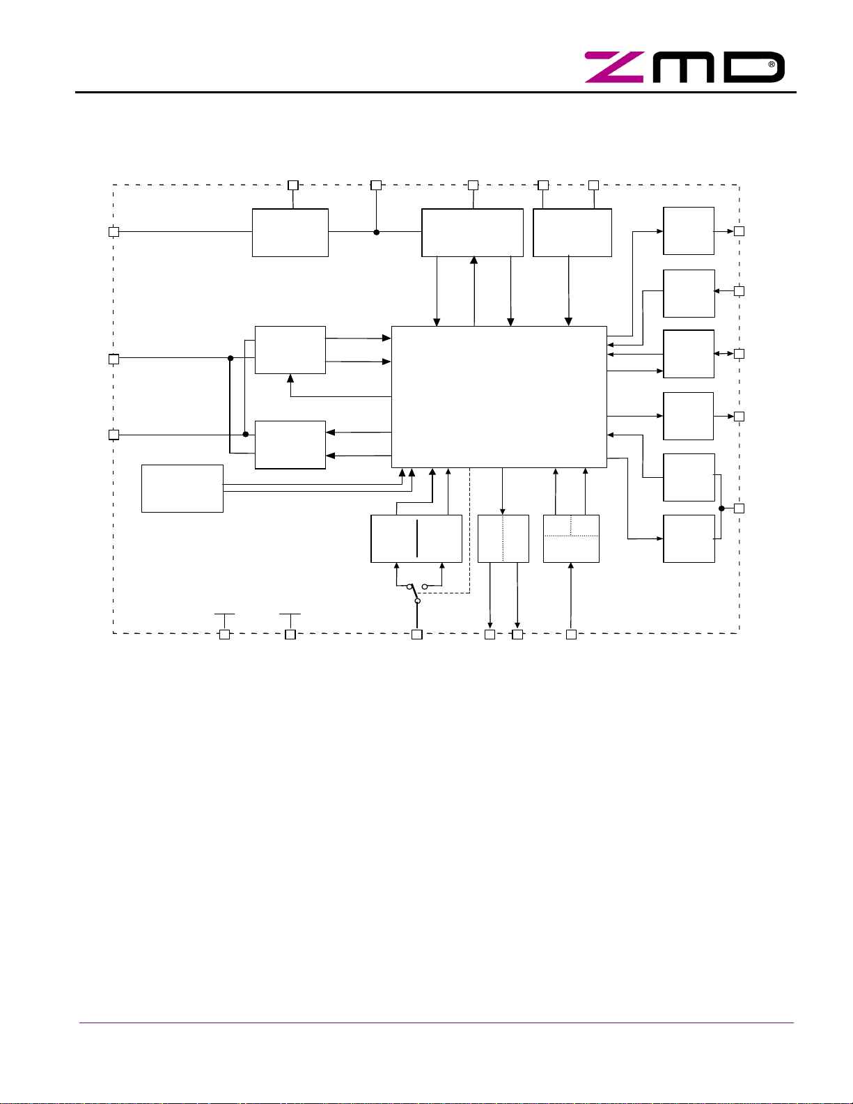
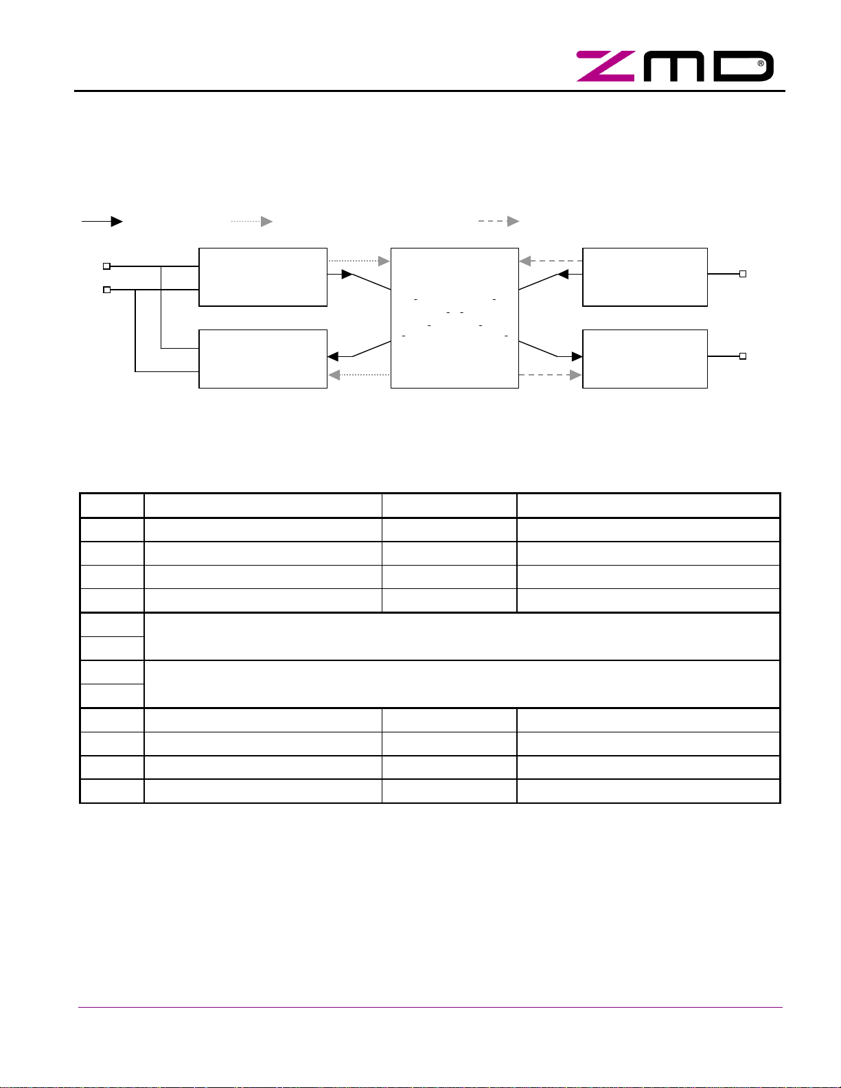
2 Basic Functional Description
2.1 Functional Block Diagram
U
IN
U
OUT
U5R
OSC1/2
CAP
ASI4U
DO(3:0)
ASIP
ASIN
THERMAL /
OVERLOAD
PROTECTION
RECEIVE
TRANSMIT
P-PULSE
N-PULSE
REC-RESET
SEND-D
SEND-SBY
OVER-LOAD
OVER-HEAT
CMOS
INPUT
STAGE
-ON
RESET
DIGITAL
IRD_IN
Current
INPUT
U5RD
-DOWN
OUT
LOGIC
LED
OUTPUT
STAGE
DATA-OUT
RESET
DATA-STRB
-IN
DI(3:0)
DSR
OUT
INPUT
STAGE
PARAM
STRB
PST
PARAM
P(3:0)
LGND
Figure 3: Functional Block Diagram
Following device functions are associated with the different blocks of the IC:
RECEIVE
The receive block converts the analog telegram waveform from the AS-i bus to a digital
pulse coded signal that can be processed further by a digital UART circuit.
The RECEIVE block is directly connected to the AS-i line pins ASIP and ASIN. It converts
the differential AS-i telegram to a single ended signal and removes the DC offset by high
pass filtering. To adapt quickly on changing signal amplitudes in telegrams from different
network users, the amplitude of the first telegram pulse is measured by a 3 bit flash ADC
and the threshold of a positive and a negative comparator is set accordingly to about 50% of
the measured level. The comparators generate the P-Pulse and N-Pulse signals.
TRANSMIT
The transmit block transforms a digital response signal to a correctly shaped send current
signal which is applied to the AS-i bus. Due to the inductive network behavior of the network
the changing send current induces voltage pulses on the network line that overlay the DC
operating voltage. The voltage pulses shall have sin²-wave shapes. Hence, the send current
shape must follow the integral of the sin²-wave function.
Copyright © 2006, ZMD AG, Rev.1.6
All rights reserved. T he material contained herein may not be reprod uced, adap ted, merged, translated, stored, or used without the prior written consent of the copyright owner. T he
Information furnished in this publication is preliminary and subject to changes without notice.
9/57

Datasheet
DIGITAL LOGIC
ELECTRONIC
INDUCTOR
POWER
SUPPLY
OSCILLATOR
THERMAL /
OVERLOAD
PROTECTION
IRD CMOS /
AC CURRENT
INPUT
ZENTRUM MIKROELEKTRONIK DRESDEN AG
“ASI for you” IC
The digital logic block contains UART, Main State Machine, E²PROM memory and other
control logic. E²PROM write access and other I/O operations of the Main State Machine are
supported in Slave Mode only (see description of general IC operational modes below). In
Master Mode the IC is basically equivalent to a physical layer transceiver.
If Slave Mode is activated, the UART demodulates the received telegrams, verifies telegram
syntax and timing and controls a register interface to the Main State Machine. After reception of a correct telegram, the UART generates appropriate Receive Strobe signals, that tell
the Main State Machine to start further processing. The Main State Machine decodes the
telegram information and starts respective I/O processes or E²PROM access. A second
register interface is used to send data back to the UART for construction of a telegram response. The UART modulates the response data into a Manchester-II-coded bit stream that
is used to control the TRANSMIT unit.
The electronic inductor is basically a gyrator circuit. It provides an inductive behavior between the IC pins UIN and UOUT while the inductance is controlled by the capacitor on pin
CAP. The inductor shall decouple the power regulator of the IC as well as the external load
circuit from the AS-i bus and hence prevent cross talk or switching noise from disturbing the
telegram communication on the bus.
The AS-i Complete Specification describes the input impedance behavior of a slave module
by an equivalent circuit that consists of R, L and C in parallel. For example, a slave module
in Extended Address Mode shall have R > 13.5 kOhm, L > 13.5 mH and C < 50pF. The
electronic inductor of the ASI4U delivers values that are well within the required ranges for
output currents up to 55mA. More detailed parameters can be found in chapter 3.17.2.
The electronic inductor requires an external capacitor of 10µF at pin UOUT for stability.
The power supply block consists of a bandgap referenced 5V-regulator as well as other
reverence voltage and bias current generators for internal use. The 5V regulator requires an
external capacitor at pin U5R of at least 1µF for stability. It can source up to 4mA for external use, however the power dissipation and the resulting device heating become a major
concern, if too much current is drawn from the regulator.
The oscillator supports direct connection of 8.000 MHz or 16.000 MHz crystals with a dedicated load capacity of 12pF and parasitic pin capacities of up to 8pF. The IC automatically
detects the oscillation frequency of the connected crystal and controls the internal clock
generator circuit accordingly.
After power-on reset the IC is set to 16.000 MHz operation by default. After about 200µs it
will either switch to 8.000 MHz operation or remain in the 16.000 MHz mode. The frequency
detection is active until the first AS-i telegram was successfully received in order to make
sure the IC found the correct clock frequency setting. The detection result is locked thereafter to increase resistance against burst or other interferences.
The oscillator unit also contains a clock watch dog circuit that can generate an unconditioned IC reset if there was no clock oscillation for more than about 20µs. This is to prevent
the IC from unpredicted behavior if no clock signal is available anymore.
The IC is self protected against thermal overheating and short circuiting of pin UOUT towards IC ground.
If the silicon die temperature rises above around 140°C for more than 2 seconds, the IC
detects thermal overheating, switches off the electronic inductor, performs an IC reset and
sets all analog blocks to power down mode. The 5V-regulator is of course also turned off in
this state, however, there will still remain a voltage of about 3 … 3.5V available at U5R that
is derived from the internal start circuitry. The overheat protection state can only be left by
power-cycling the AS-i voltage.
Shortcutting pin UOUT towards IC ground leads to the same IC behavior as thermal overheating.
The IRD pin is input for the additional addressing channel in Slave Mode (see description of
General IC Operational Modes below) or direct AS-i transmitter input in Master Mode. In
Slave Mode it can be operated either in CMOS Mode or AC-current input mode. The later is
provided for direct connection of a photo diode. More detailed information can be found in
Copyright © 2006, ZMD AG, Rev.1.6
All rights reserved. The material contained herein may not be repr oduced, ad apted, merged, translated, stored, or used without the prior written consent of the copyright o wner. T he
Information furnished in this publication is preliminary and subject to changes without notice.
10/57

Datasheet
ZENTRUM MIKROELEKTRONIK DRESDEN AG
“ASI for you” IC
chapter 3.3 Addressing Channel Input IRD.
FID DIGITAL /
ANALOG
STAGE
INPUT STAGE
Pin FID can be set to digital CMOS mode or analog voltage input mode. In Slave Mode it is
set to CMOS operation, in Master Mode it works in analog mode and acts as input for the
power fail comparator.
All digital inputs, except of the oscillator pins, have high voltage capabilities and partly
Schmitt-Trigger and Pull-Up features. For more details see chapter 3.4 Digital Inputs - DC
Characteristics.
OUTPUT
STAGE
All digital output stages, except of the oscillator pins, have high voltage capabilities and are
implemented as NMOS open drain buffers. Each pin can sink up to 10mA of current.
2.2 General Operational Modes
The ASI4U provides two main and two additional sub operational modes. Main operation modes divide in
Slave Mode and Master Mode. Sub operation modes divide in Repeater Mode and Monitor Mode. The later
were derived from Master Mode in providing different output signals at the Parameter Port.
A definition of which operational mode becomes active is made by programming the flags Master_Mode and
Repeater_Mode in the Firmware Area of the E²PROM (see also Table 7 on page 18). The E²PROM is read out
at every initialization of the IC. Online mode switching is not provided. The following configurations apply:
Table 5: Assignment of operational modes
Selected Operational Mode Master Mode Flag Repeater Mode Flag
Slave Mode 0 0
Master Mode 1 0
Repeater Mode 1 1
Monitor Mode 0 1
In Slave Mode the ASI4U operates as fully featured AS-i Slave IC according to AS-i Complete Specification
v3.0.
In Master Mode the ASI4U translates a digital output signal from the master control logic (etc. PLC, µP, …) to a
correctly shaped, analog AS-i pulse sequence and vice versa. Every AS-i telegram received is checked for consistency with the AS-i communication protocol specifications and if no errors were found, an appropriate receive
strobe signal is generated.
Master Mode and Monitor Mode differ in the kind of signaled telegrams. In Master Mode a single Receive
Strobe signal is provided validating every correctly received Slave Response while in Monitor Mode two different
Receive Strobe signals are available displaying every correctly received Master and Slave telegram separately.
The Monitor Mode is intended for use in intelligent slaves and bus monitors that provide own telegram decoding
mechanisms but do not check for correct telegram timing or syntax.
The Repeater Mode is specifically provided for AS-i bus repeater applications.
2.3 Slave Mode
The Slave Mode is probably the most complex operational mode of the IC. The ASI4U does not only support all
mandatory AS-i Slave functions but also a variety of additional features that shall make AS-i Slave module design very easy and flexible.
2.3.1 AS-i communication channel
In slave mode the ASI4U can work on two different communication channels, the AS-i channel and the IRD
channel. The AS-i channel is directly connected to AS-i Bus via the pins ASIP and ASIN. A receiver and a
transmitter unit are connected in parallel to the pins that allow fully bi-directional communication through ASIP
and ASIN.
Copyright © 2006, ZMD AG, Rev.1.6
All rights reserved. T he material contained herein may not be reprod uced, adap ted, merged, translated, stored, or used without the prior written consent of the copyright owner. T he
Information furnished in this publication is preliminary and subject to changes without notice.
11/57
ASI+
ASI
-
i IC
ASI+
Datasheet
ZENTRUM MIKROELEKTRONIK DRESDEN AG
“ASI for you” IC
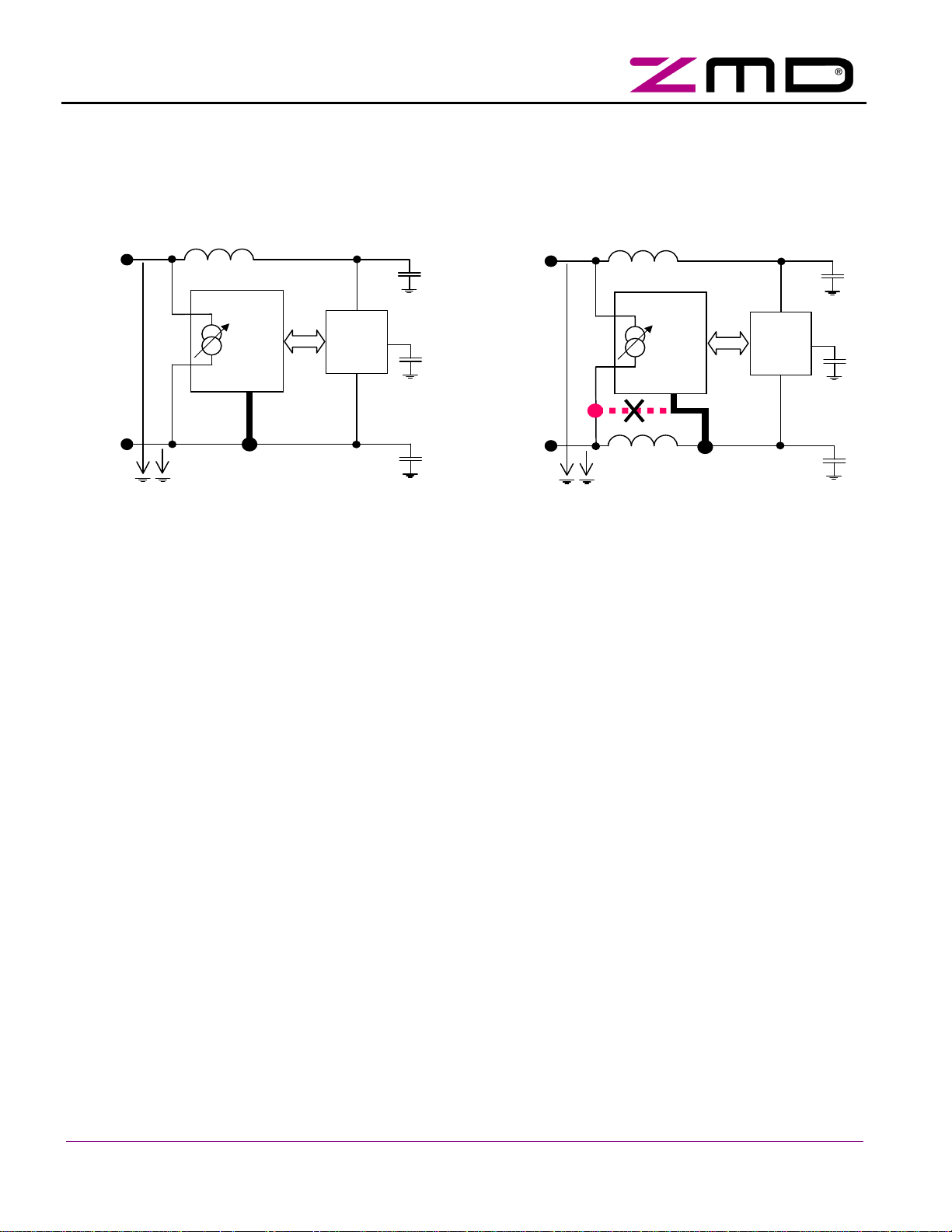
The ASI4U is the first IC that supports floating operation of the AS-i receiver and transmitter (within certain limits) in relation to IC ground. Thus far, the ASIN pin always had to be on the same potential like IC ground, preventing full symmetrical input circuits with external coils. The following figures illustrate the new functionality. If
one compares the relation Z1 / Z2, which is a measure for symmetry of the AS-i module input towards machine
ground, it becomes obvious that the new circuit is more symmetrical since Z1 and Z2 are more equal than in the
conventional solution. Please note, that this is not a complete application circuit.
Z1
AS-i
Slave
IC
Load
Z1
AS-i
Slave
IC
Load
GND
GND
Z2
ASI-
Z2
Figure 5: Conventional application of AS-i IC
with one external coil
Figure 4: Newly supported application of AS-
with two external coils
2.3.2 IRD communication channel
Besides the AS-i communication channel the ASI4U can also operate on a second input channel, the so called
IRD Input Channel or Addressing Channel. In this mode the IRD pin is input for an AS-i signal in Manchester-IIcoded format. The signal can either be an AC-current signal generated by a photo diode or a 5V-CMOS signal.
The IC automatically detects the type of the signal and switches the input path accordingly.
Output pin in IRD communication mode is LED1. It transmits the slave response as inverted Manchester-IIcoded AS-i signal. The red LED, which is normally connected to LED1, can form the response transmitter in an
optical communication system or LED1 can be directly connected to some external circuitry.
Activation of the IRD communication channel is achieved by a so called magic sequence, that is sent in advance of the desired communication. The construction of a magic sequence is described in detail in chapter 3.3
Addressing Channel Input IRD on page 22. The IRD communication mode is basically left by IC reset, except in
one special case that is also described in that chapter.
2.3.3 Parameter Port Pins
The ASI4U features a 4-bit wide parameter port and a related parameter strobe signal pin PST. There is a defined phase relation between a parameter output event, the parameter input sampling and the activation of the
PST signal. Thus it can be used to trigger external logic or a micro controller to process the received parameter
data or to provide new input data for the AS-i slave response.
AS-i Complete Specification V3.0 newly defines a bidirectional mode for parameter data. The ASI4U supports
this feature, that can be activated by special E²PROM setting.
See chapter 3.6 Parameter Port and PST on page 26 for further details.
2.3.4 Data Port Pins
An important feature of the ASI4U is the 8-bit wide data port that consists of a 4-bit wide input section and a 4bit wide output section. The input and output sections work independently from each other allowing a maximum
of 8 devices (4 input and 4 output devices) to be connected to the ASI4U. For special applications (compatibility), the so called Multiplex Mode can be activated that limits the output activation to a certain time frame. Thus,
a 4-bit wide bi-directional data I/O Port can be realized by external connection of the corresponding data input
and output pins.
Copyright © 2006, ZMD AG, Rev.1.6
All rights reserved. The material contained herein may not be repr oduced, ad apted, merged, translated, stored, or used without the prior written consent of the copyright o wner. T he
Information furnished in this publication is preliminary and subject to changes without notice.
12/57

Datasheet
ZENTRUM MIKROELEKTRONIK DRESDEN AG
“ASI for you” IC
The data port is accompanied by the data strobe signal DSR. There is a defined phase relation between a data
output event, the input data sampling and the activation of the DSR signal. Thus, it can be used to trigger external logic or a micro controller to process the received data or to provide new input data for the AS-i slave response. See chapter 3.7 Data Port and DSR on page 29 for further details.
2.3.5 Data Input Inversion
By default the logic signal (HIGH / LOW) that is present at the data input pins during the input sampling phase is
transferred without modification to the send register, which is interfaced by the UART. By that, the signal becomes directly part of the slave response.
Some applications work with inverted logic levels. To avoid additional external inverters, the input signal can be
inverted by the ASI4U before transferring it to the send register. The inversion of the input signals can either be
done bit selective or jointly for all data input pins. See chapter 3.7.2 Input Data Pre-Processing on page 30.
2.3.6 Data Input Filtering
To prevent input signal bouncing from being transferred to the AS-i Master, the data input signals can be digitally filtered. Filter times can be configured in 7 steps from 128µs up to 8.192ms. Additionally there is a so called
AS-i Cycle Mode available. If activated, the filter time is determined by the actual AS-i cycle time. For more detailed information refer to chapter 3.7.2 Input Data Pre-Processing on page 30.
The filter function can be enabled bit selective. Activation of the filters is done jointly either by E²PROM configuration or by the logic state of parameter port pin P2. See chapter 3.7.2 Input Data Pre-Processing on page 30.
2.3.7 Fixed Data Output Driving
The fixed data output driving feature is thought to ease board level design for similar products that do not require the full data output port width. The user can select one or more bits from the data output port to be driven
by a distinct logic level instead by the data that was sent by the master. The distinct output data is stored in the
E²PROM and can be set during final module configuration. Thus it is possible to signal the actual IC profile to
some external circuitry and to allow reuse of certain board designs for different product applications.
See chapter 3.7.3 Fixed Output Data Driving on page 32 for further details.
2.3.8 Synchronous Data I/O Mode
AS-i Complete Specification V3.0 newly defines a synchronous data I/O feature, that allows a number of slaves
in the network to switch their outputs at the same time and to have their inputs sampled jointly. This feature is
especially useful if more than 4-bit wide data is to be provided synchronously to an application.
The synchronization point was defined to the data exchange event of the slave with the lowest address in the
network. This definition relies on the cyclical slave polling with increasing slave addresses per cycle that is one
of the basic communication principles of AS-i. The IC always monitors the data communication and detects the
change from a higher to a lower slave address. If such a change was recognized, the IC assumes that the slave
with the lower address has the lowest address in the network.
There are some special procedures that become active during the start of synchronous I/O mode operation and
if more than three consecutive telegrams were sent to the same slave address. This is described in more detail
in chapter 3.7.4 Synchronous Data I/O Mode on page 32.
2.3.9 4 Input / 4 Output processing in Extended Address Mode
A new feature of AS-i Complete Specification v3.0 is also support of 4-bit wide output data in Extended Address
Mode. In Extended Address Mode it was, up to Complete Specification v2.11, only possible to send three data
output bits from the master to the slave because telegram bit I3 is used to select between A- and B- slave type
for extended slave addressing (up to 62 slaves per network). In normal address mode I3 carries output data for
pin D3.
The new definition introduces a multiplexed data transfer, so that all 4-bits of the data output port can be used
again. A first AS-i cycle transfers the data for a 2-bit output nibble only, while the second AS-i cycle transfers the
data for the contrary 2-bit nibble. Nibble selection is done by the remaining third bit. To ensure continuous alternation of bit information I2 and thus continued data transfer to both nibbles, a special watchdog was implemented that observes the state of I2 bit. The watchdog can be activated or deactivated by E²RPOM setting. It
provides a watchdog filter time of about 327ms.
Copyright © 2006, ZMD AG, Rev.1.6
All rights reserved. T he material contained herein may not be reprod uced, adap ted, merged, translated, stored, or used without the prior written consent of the copyright owner. T he
Information furnished in this publication is preliminary and subject to changes without notice.
13/57

Datasheet
ZENTRUM MIKROELEKTRONIK DRESDEN AG
“ASI for you” IC
The multiplexed transfer of course increases the refresh time per output by a factor of two, however, some applications can tolerate this increase for the benefit of less external circuitry and better slave address efficiency.
The sampling cycle of the data inputs remains unchanged since the meaning of I3 bit was not changed in the
slave response with the definition of the Extended Address Mode.
More detailed information is described in chapter 3.7.5 Support of 4I/4O processing in Extended Address Mode,
Profile 7.A.x.E on page 34.
2.3.10 AS-i Safety Mode
The enhanced data input features described above require additional registers in the data input path that store
the input values for a certain time before they hand them over to the AS-i transmitter. This causes a time delay
in the input path that could lead to a delayed “turn off” event, if the registers were activated by intention or by
accident in AS-i Safety Applications.
To safely exclude an activation of the enhanced data I/O features in Safety Applications, the IC provides a special Safety Mode that is strongly recommended to be used for AS-i Safety communication purposes. See chapter 3.7.6 Safety Mode Operation on page 34 for further details.
2.3.11 Enhanced LED Status Indication
ASI4U newly supports enhanced status indication by two LED outputs. A special mode for direct application of
Dual-LEDs and the respective different signaling modes is also implemented. Compared to the A²SI, the former
U5RD pin was reassigned as LED2 pin. Thus, compatibility to existing A²SI board layouts is still guaranteed.
However, it will require to keep LED2 pin disabled (default state at delivery) in order to avoid short-circuiting of
U5R to ground. More detailed information on the different signaling schemes and their activation can be found in
chapter 3.9 LED outputs on page 40.
2.3.12 Communication Monitor/Watchdog
Data and Parameter communication are continuously observed by a communication monitor. If neither
Data_Exchange nor Write_Parameter calls were addressed to and received by the IC within a time frame of
about 41ms, a so called No Data/Parameter Exchange status is detected and signaled at LED1.
If the respective flags are set in the E²PROM the communication monitor can also act as communication watchdog, that initiates a complete IC reset after expiring of the watchdog timer. The watchdog mode can also be
activated and deactivated by a signal at parameter port pin P0. For more detailed information see chapter 3.14
Communication Monitor/Watchdog on page 47.
2.3.13 Write protection of ID_Code_Extension_1
As defined in AS-i Complete Specification v3.0 the ASI4U also supports write protection for ID_Code_Extension_1. The feature allows the activation of new manufacturer protected slave profiles and is enabled by
E²PROM setting. It is described in more detail in chapter 3.16 Write Protection of ID_Code_Extension_1 on
page 47
2.3.14 Summary of Master Calls
Table 6 on page 15 and the diagram at the following page show the complete set of Master Calls that are decoded by the ASI4U in Slave Mode. The "Enter Program Mode" call is intended for programming of the IC by
the slave manufacturer only. It becomes deactivated as soon as the Program_Mode_Disable flag is set in the
Firmware Area of the E²PROM.
AS-i Complete Specification compliance note:
In order to achieve full compliance to the AS-i Complete Specification, the Program_Mode_Disable flag must be
set by the manufacturer of AS-i slave modules during the final manufacturing and configuration process and
before an AS-i slave device is delivered to field application users.
Copyright © 2006, ZMD AG, Rev.1.6
All rights reserved. The material contained herein may not be repr oduced, ad apted, merged, translated, stored, or used without the prior written consent of the copyright o wner. T he
Information furnished in this publication is preliminary and subject to changes without notice.
14/57
Code_1
1
Configuration
0
0
0
0
1
Datasheet
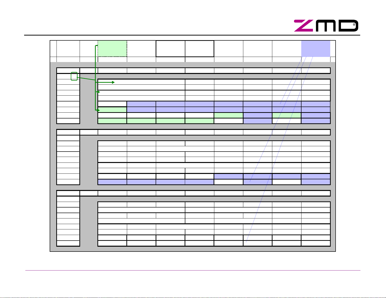
Instruction MNE ST CB A4 A3 A2 A1 A0 I4 I3 I2 I1 I0 PB EB SB I3 I2 I1 I0 PB EB
Data Exchange
Write Parameter
ZENTRUM MIKROELEKTRONIK DRESDEN AG
“ASI for you” IC
Table 6: ASI4U Master Calls and Related Slave Responses
Master Request Slave Response
DEXG 0 0 A4 A3 A2 A1 A0 0
WPAR 0 0 A4 A3 A2 A1 A0 1
D3
D2 D1 D0 PB 1 0
~Sel
P3
P2 P1 P0 PB 1 0
~Sel
D3 E3D2 E2D1 E1D0
E0
P3 I3P2 I2P1 I1P0
I0
PB 1
PB 1
Address Assignment
Write Extented ID
Delete Address
Reset Slave
Read IO
Read ID Code
Read ID Code_1
Read ID Code_2
Read Status
Broadcast (Reset)
Enter Program Mode
ADRA 0 0 0 0 0 0 0 A4 A3 A2 A1 A0 PB 1 0 0 1 1 0 0 1
WID1 0 1 0 0 0 0 0 0 ID3 ID2 ID1 ID0 PB 1 0 0 0 0 0 0 1
DELA 0 1 A4 A3 A2 A1 A0 0 0 Sel 0 0 0 PB 1 0 0 0 0 0 0 1
RES 0 1 A4 A3 A2 A1 A0 1
RDIO 0 1 A4 A3 A2 A1 A0 1
RDID 0 1 A4 A3 A2 A1 A0 1
RID1 0 1 A4 A3 A2 A1 A0 1
RID2 0 1 A4 A3 A2 A1 A0 1
RDST 0 1 A4 A3 A2 A1 A0 1
~Sel
~Sel
1 0 0 PB 1 0 0 1 1 0 0 1
0 0 0 PB 1 0 IO3 IO2 IO1 IO0 PB 1
Sel
0 0 1 PB 1 0 ID3 ID2 ID1 ID0 PB 1
Sel
0 1 0 PB 1 0 ID3 ID2 ID1 ID0 PB 1
Sel
0 1 1 PB 1 0 ID3 ID2 ID1 ID0 PB 1
Sel
1 1 0 PB 1 0 S3 S2 S1 S0 PB 1
BR01 0 1 1 1 1 1 1 1 0 1 0 1 1 1 --- no slave response ---
PRGM 0 1 0 0 0 0 0 1 1 1 0 1 1 1 --- no slave response ---
Note: In Extended Address Mode the "Select Bit" defines whether the A-Slave or B-Slave is being addressed. Depending on the type of master call bit I3 carries the
select bit information (Sel = A-Slave) or the inverted select bit information (~Sel = B-Slave).
Copyright © 2006, ZMD AG, Rev.1.6
All rights reserved. The material contained herein may not be reproduced, adapted, merged, translated, stored, or used without the prior written consent of the copyright owner. The Information furnished in this publication is preliminary and subject to changes without notice.
15/57
B-Slave with
ASI Master
ASI Slave
Response (blue
ADR != 0
I2 I1 I0
000
001
010
011
100
101
110
111
CB I4
I3
I3=Sel
(Slave Address != 0) AND (Progam Mode not activated)
001
Sel=1
101
Sel=1
110
Sel=0
Broadcast
111
Sel=1
ADR == 0
I2 I1 I0
000
001
010
011
100
101
110
111
CB I4 I3
(Slave Address == 0) AND (Progam Mode not activated)
011
101
110
Broadcast
111
I2 I1 I0
000
001
010
011
100
101
110
111
CB I4 I3
Progam Mode activated
001
011
16/57
Datasheet
ZENTRUM MIKROELEKTRONIK DRESDEN AG
“ASI for you” IC
No Slave
Profile 0.A
(green shaded)
Request
(black/green)
Response
(blue)
shaded)
000 Sel=0
010 Sel=0
011 Sel=1
100 Sel=0
000
001
010
100
000
010
100
101
110
111
Data_Exchange /Sel D2 D1 D0
Data_Exchange D3 D2 D1 D0 D3 D2 D1 D0
Write_Parameter /Sel P2 P1 P0
Write_Parameter P3 P2 P1 P0 P3 P2 P1 P0
Delete_Addr x0
Delete_Addr x0
Rd_IO_Cfg <I3:I0> Read_ID <I3:I0> Read_ID_1<I3:I0> Read_ID_2 <I3:I0> Reset_Slave 0x6
Rd_IO_Cfg <I3:I0> Read_ID <I3:I0> Read_ID_1<I3:I0> Read_ID_2 <I3:I0> Reset_Slave 0x6 Rd_Status
Address_Assignment A4 A3 A2 A1 A0
0x6
Write_Var_Ext_Code1 ID3 ID2 ID1 ID0
0x0
Rd_IO_Cfg <I3:I0> Read_ID <I3:I0> Read_ID_1<I3:I0> Read_ID_2 <I3:I0>
Reset_Slave 0x6
Data_Exchange - - - - I3 I2 I1 I0 (EEPROM READ ACCESS)
Write_Parameter I3 I2 I1 I0 I3 I2 I1 I0 (EEPROM WRITE ACCESS)
Write_Var_ID_Code ID3 ID2 ID1 ID0
0x0
Rd_IO_Cfg <I3:I0> Read_ID <I3:I0> Read_ID_1<I3:I0> Read_ID_2 <I3:I0> Reset_Slave 0x6
Rd_IO_Cfg <I3:I0> Read_ID <I3:I0> Read_ID_1<I3:I0> Read_ID_2 <I3:I0> Reset_Slave 0x6
EnterPmode
Broadcast
EnterPmode
Rd_Status
Rd_Status
Rd_Status
Rd_Status
<S3:S0>
<S3:S0>
<S3:S0>
<S3:S0>
<S3:S0>
reserved
reserved
Copyright © 2006, ZMD AG, Rev.1.6
All rights reserved. The material contained herein may not be reproduced, adapted, merged, translated, stored, or used without the prior written consent of the copyright owner. The Information furnished in this publication is preliminary and subject to changes without notice.
ASI+
ASI
-
Datasheet
ZENTRUM MIKROELEKTRONIK DRESDEN AG
“ASI for you” IC
2.4 Master Mode
Master Mode and the related Repeater- and Monitor-Modes differ completely in their functional properties from
the Slave Mode. While the IC can autonomously perform different tasks in Slave Mode, it will only act as physical layer transceiver in Master-, Repeater- and Monitor-Mode. The basic property of these modes is a modulation / demodulation of AS-i signals to Manchester-II-code and vice versa. The following figure shows the different data path configurations.
Master Mode Slave Mode, ASI-Channel Slave Mode, IRD Addressing Channel
ASI- Receiver
UART
ASI- Transmitter
Figure 6:
Data path in Master-, Repeater- and Monitor-Mode
Master-Mode, Repeater-Mode and Monitor-Mode differ from each other in the kind of signals that are available
at the data I/O and parameter port pins of the IC. Following signal assignments are provided:
IRD CMOS
Input
LED Output
IRD
(TX)
LED1
(RX)
Pin Master Mode Repeater Mode Monitor Mode
P0 Receive Clock Hi-Z Receive Clock
P1 Power Fail Hi-Z Power Fail
P2 Receive Strobe – Slave Telegram Hi-Z Receive Strobe – Slave Telegram
P3 Hi-Z Hi-Z Receive Strobe – Master Telegram
DI0
DI1
DI2
DI3
Inverting of IRD input signal. If both inputs are on different level, the IRD input signal is inverted
before further processing, otherwise it is directly forwarded to the UART.
Inverting of LED output signal. If both inputs are on different level, the LED output signal is inverted after processing, otherwise it is directly forwarded to the LED1 output.
DO0 Hi-Z Hi-Z Pulse Code Error
DO1 Hi-Z Hi-Z No Information Error
DO2 Hi-Z Hi-Z Parity Bit Error
DO3 Hi-Z Hi-Z Manchester-II-Code Error at IRD Input
More detailed signal descriptions can be found in chapters 3.6 Parameter Port and PST, 3.7 Data Port and DSR
as well as 3.12 UART.
Copyright © 2006, ZMD AG, Rev.1.6
All rights reserved. T he material contained herein may not be reprod uced, adapted, merged, translated, stored, or used without the pri or wri tten co nsent of the co pyright owner. The
Information furnished in this publication is preliminary and subject to changes without notice.
17/57

tion
ctional Parameter Port
Watchdog can be activated/deactivated by
Communication watchdog is continuously
Datasheet
ZENTRUM MIKROELEKTRONIK DRESDEN AG
“ASI for you” IC
2.5 E²PROM
The ASI4U provides an on-chip E²PROM with typical write times of 12.5 ms and read times of 110ns. For security reasons the memory area is structured in two independent data blocks and a single bit Security flag.
The data blocks are named User Area and Firmware Area. The Firmware Area contains all manufacturing related configuration data (i.e. selection of operational modes, ID codes, …). It can be protected against undesired
data modification by setting the Program_Mode_Disable flag to ‘1’.
The User Area contains only such data that is relevant for changes at the final application (i.e. field installation
of slave module). The environment, where modifications of the user data may become necessary, can sometimes be rough and unpredictable. In order to ensure a write access cannot result in an undetected corruption of
E²PROM data, additional security is provided when programming the User Area.
Any write access to the User Area (by calls Address_Assignment or Write_ID_Code1) is accompanied by two
write steps to the Security flag, one before and one after the actual modification of user data.
The following procedure is executed when writing to the User Area of the E²PROM:
1. The Security flag is programmed to ‘1’.
2. The content of the Security flag is read back, verifying it was programmed to ‘1’.
3. The user data is modified.
4. A read back of the written data is performed.
5. If the read back has proven successful programming of the user data, the Security flag
is programmed back to ‘0’.
6. The content of the Security flag is read back, verifying it was programmed to ‘0’.
In addition to a read out of the data areas, the Security flag of the E²PROM is also read and evaluated during IC
initialization. In case the value of the Security flag equals ‘1’ (i.e. due to an undesired interruption of a User Area
write access), the entire User Area data is treated as corrupted and the Slave Address is set to 0x0 in the corresponding volatile shadow registers during initialization. Thus the programming of the User Area data can be
repeated.
Table 7: E²PROM Content
ASI4U internal
E²PROM Address [hex]
Bit
Position
0 0 … 3
1 0
2 0 … 2
2 3
3 … 7
8 0 … 3
9 0 … 3
A 0 … 3
B
0
1
2
3
EEPROM Cell Content EEPROM Register Content
A0 … A3
A4
Slave address low nibble
Slave address high nibble
ID1_Bit0 … ID1_Bit2 ID_Code_Extension_1
ID1_Bit3 ID_Code_Extension_1, A/B slave selec
in extended address mode
Not implemented
ID_Bit0 … ID_Bit3 ID_Code
ID2_Bit0 … ID2_Bit3 ID_Code_Extension_2
IO_Bit0 … IO_Bit3 IO_Code
Multiplex_Data
Multiplex_Paramter
Multiplexed bi-directional Data Port mode
Multiplexed bi-dire
mode
P0_Watchdog_Activation
the logic value at parameter pin P0.
Watchdog_Active must not be set.
Watchdog_Active
activated.
Copyright © 2006, ZMD AG, Rev.1.6
All rights reserved. The material contained herein may not be repr oduced, ad apted, merged, translated, stored, or used without the prior written consent of the copyright o wner. The
Information furnished in this publication is preliminary and subject to changes without notice.
18/57
 Loading...