

ZMD A2SI-Lite 14, A2SI-Lite 16 DATA SHEET
A²SI-Lite 14 / A²SI-Lite 16
Data Sheet
Low End Device AS-Interface IC
1 Features
• Fully operable in AS-interface networking
systems and capable of working in extended
networks with up to 62 slaves (V2.11)
• Dedicated IO-port structure: two data inputs, two
data outputs, no parameter port pins
• Integrated EEPROM stores relevant AS-i
information and IC configuration data (e.g. enabling/disabling of the PWM feature)
• Programmable PWM of output signals can be
used to control intensity of driven LEDs
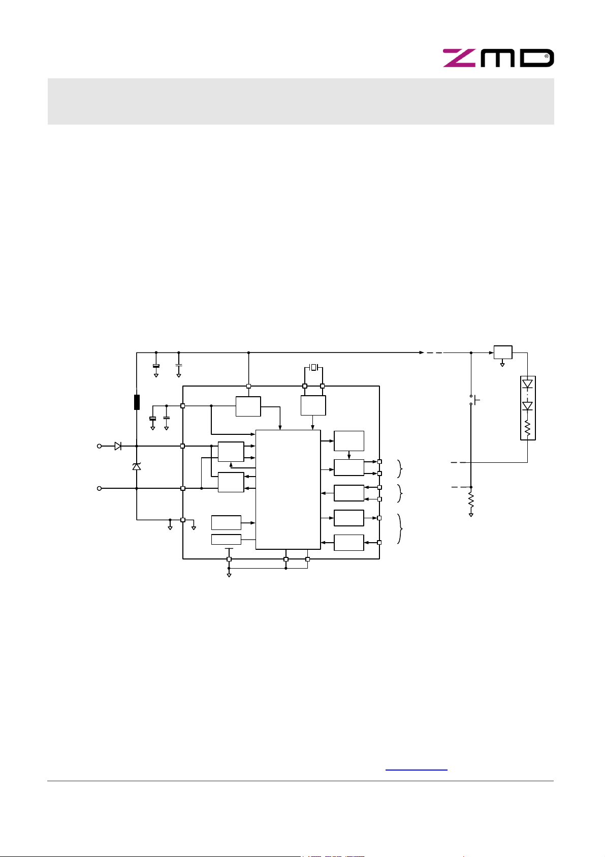
3 Block Diagram
10uF
100nF
VIN
18 mH
ASI+
ASI-
AS-i network
cable access
CAP
100nF
1uF
ASIP
ASIN
0V
5V
Receiver
Trans-
mitter
Thermal
Protection
EEPROM
GND
Power
Supply
Power on
Reset
DIGITAL
LOGIC
UART
State Machine
Ports
TEST1 TEST2
OSC1
2 Description
This integrated circuit shall be used as simplified
interface IC for key control panels, simple sensors
and small actuators based on the AS-i
specifications. The device shall be in compliance
with AS-i Specification V2.11. The IC performs
multiple interface functions.
There are two package options; the 14 pin SOP
option A²SI-Lite 14 (A²SI-L14) and the 16 pin SOP
option A²SI-Lite 16 (A²SI-L16). In contrast to the
A²SI-L14 IC the A²SI-L16 IC has two more pins; a
diagnostic LED output pin (LED pin) and a fault
indicator input pin (FID pin).
Voltage
Regulator
16MHz
Oscillator
OSC2
A²SI-L14
A²SI-L16
Pulse
Width
Modulation
Output
Stages
Input
Stages
Output
Stages
Input
Stages
DO0
DO1
DI2
DI3
LED
FID
Slave electronics
supply voltage
Two outputs, e.g.
interconnced to push
button LEDs
Two inputs, e.g.
interconnced to push
button contacts
diagnostic pins,
available at A²SIL16 version only
Switch
GND
LED-Lamp
24V
Application
Figure 3-1: Block Diagram
4 Application Support
Configuration of the chip is handled through programming of the on-chip E²PROM. ZMD provides a
special
AS-Interface Programmer Tool
(Ordering Code: 3000003356 )
to ease product evaluation and selection of different operation modes.
Further application support is available through e-mail hotline under asi@zmd.de
Rev. 2.0, Copyright © 2005, ZMD AG
All rights reserved. The material contained herein may not be reproduced, adapted, merged, translated, stored, or used without the prior written consent of the copyright owner. The
Information furnished in this publication is preliminary and subject to changes without notice.
1/22

A²SI-Lite 14 / A²SI-Lite 16
Data Sheet
Low End Device AS-Interface IC
Table of Contents Page
1 FEATURES ....................................................................................................................................................1
2 DESCRIPTION ...............................................................................................................................................1
3 BLOCK DIAGRAM ........................................................................................................................................1
4 APPLICATION SUPPORT.............................................................................................................................1
5 PIN DESCRIPTION ........................................................................................................................................4
6 PIN CONFIGURATION ..................................................................................................................................4
7 ELECTRICAL SPECIFICATION....................................................................................................................5
7.1 ABSOLUTE MAXIMUM RATINGS (NON OPERATING) ......................................................................................5
7.2 RECOMMENDED OPERATING CONDITIONS...................................................................................................6
7.3 QUALITY ASSURANCE ................................................................................................................................6
7.4 DC AND AC CHARACTERISTIC OF ALL PINS AND FUNCTIONS........................................................................6
7.4.1 Digital input and output Pins ............................................................................................................7
7.4.2 AS-i Bus Load (Pins ASIP/ASIN and Power Supply Input VIN) ......................................................8
7.4.3 Pins OSC1, OSC2 ...........................................................................................................................8
7.5 INFORMATION DATA FOR DEVELOPMENT .....................................................................................................8
8 FUNCTIONAL DESCRIPTION ....................................................................................................................10
8.1 FUNCTIONAL BLOCK DIAGRAM..................................................................................................................10
8.2 POWER SUPPLY ......................................................................................................................................10
8.3 RECEIVER ...............................................................................................................................................10
8.4 TRANSMITTER .........................................................................................................................................10
8.5 DIGITAL LOGIC.........................................................................................................................................11
8.6 DATA I/O PORTS .....................................................................................................................................12
8.6.1 Data Exchange Model....................................................................................................................12
8.6.2 PWM Function ...............................................................................................................................12
8.7 FID INPUT AND LED OUTPUT PORTS .......................................................................................................14
9 TYPICAL APPLICATION CIRCUIT OF A²SI-L ...........................................................................................15
10 PACKAGE OUTLINE AND DEVICE MARKING .....................................................................................16
11 ORDERING INFORMATION ....................................................................................................................17
12 APPLICATION SUPPORT .......................................................................................................................18
12.1 AS-INTERNATIONAL ASSOCIATION ........................................................................................................18
12.2 ZMD ...................................................................................................................................................18
12.3 ZMD APPLICATION SUPPORT PARTNERS ..............................................................................................18
13 ZMD SALES CONTACTS ........................................................................................................................18
14 ZMD DISTRIBUTION PARTNERS ..........................................................................................................19
Rev. 2.0, Copyright © 2005, ZMD AG
All rights reserved. The material contained herein may not be reproduced, adapted, merged, translated, stored, or used without the prior written consent of the copyright owner. The
Information furnished in this publication is preliminary and subject to changes without notice.
2/22

A²SI-Lite 14 / A²SI-Lite 16
Data Sheet
Low End Device AS-Interface IC
APPENDIX A: CRYSTAL PARAMETER ...............................................................................................20
A.1 PARAMETER DATA OF CRYSTAL.....................................................................................................................20
A.2 CAPACITANCE ON PCB ................................................................................................................................20
APPENDIX B: EXTERNAL COIL ...........................................................................................................21
B.1 TARGET COIL ..........................................................................................................................................21
B.2 COIL MODELING ......................................................................................................................................21
B.3 ELECTRONIC INDUCTOR ...........................................................................................................................21
APPENDIX C: EEPROM ........................................................................................................................22
List of Figures Page
Figure 3-1: Block Diagram ....................................................................................................................................1
Figure 5-1: SOIC16 Pin out ...................................................................................................................................4
Figure 5-2: SOIC14 Pin out ...................................................................................................................................5
Figure 6-1: Data Input Schematic in Principle ....................................................................................................7
Figure 6-2: Data Output Schematic in Principle .................................................................................................7
Figure 6-3: Receiver comparator threshold set-up in principle........................................................................9
Figure 6-4: Reset Behavior ...................................................................................................................................9
Figure 7-1: Functional Block Diagram...............................................................................................................10
Figure 7-2: A²SI-L IC Data Exchange master call data model .........................................................................12
Figure 7-3: PWM control .....................................................................................................................................13
Figure 7-4: PWM Output Signal Timing .............................................................................................................14
Figure 8-1: Typical Application of A²SI-L14 IC .................................................................................................15
Figure 8-2: Typical Application of A²SI-L16 IC .................................................................................................15
Figure 9-1: SOIC Package Outline Dimensions................................................................................................16
Figure 9-2: Mark Diagram of 14 Pin SOIC Version ...........................................................................................17
Figure 9-3: Mark Diagram of 16 Pin SOIC Version ...........................................................................................17
Figure A-1: Crystal oscillator equivalent circuit...............................................................................................20
Figure B-1: External Coil equivalent circuits....................................................................................................21
List of Tables Page
Table 4-1: A²SI-L14/ A²SI-L16 Pin Description ....................................................................................................4
Table 6-1: Absolute Maximum Ratings................................................................................................................5
Table 6-2: Recommended Operating Conditions ...............................................................................................6
Table 6-3: Crystal Properties
Table 6-4: Input Voltages and Currents: Pins DI2, DI3, FID, TEST1/2
Table 6-5: Output Voltages and Currents: Pins DO0, DO1, LED ......................................................................8
Table 6-6: AS-i Bus Interface Properties.............................................................................................................8
Table 6-7: Oscillator Pins......................................................................................................................................8
Table 6-8: Information Data ..................................................................................................................................8
Table 7-1: A²SI-L Master Calls and Related Slave Responses........................................................................11
Table 7-2: PWM specification of Outputs: Pins DO0, DO1..............................................................................13
Table 9-1: Package Outline Dimensions ...........................................................................................................17
Table A-1: 16 MHz crystals .................................................................................................................................20
Table A-2: Crystal models...................................................................................................................................20
Table C-1: Contents of the A²SI-L14 / A²SI-L16 EEPROM................................................................................22
1
...............................................................................................................................6
1
............................................................7
Rev. 2.0, Copyright © 2005, ZMD AG
All rights reserved. The material contained herein may not be reproduced, adapted, merged, translated, stored, or used without the prior written consent of the copyright owner. The
Information furnished in this publication is preliminary and subject to changes without notice.
3/22
A²SI-Lite 14 / A²SI-Lite 16
Data Sheet
Low End Device AS-Interface IC
5 Pin Description
Table 5-1 shows the pin description for both the A²SI-L14 and the A²SI-L16 IC. The graphical representation
(pin-out symbols) are shown in chapter 6.
Table 5-1: A²SI-L14/ A²SI-L16 Pin Description
Pin#
SOIC16
Pin#
SOIC14
Name Description
1 1 ASIPOS positive ASI supply, high voltage supply
2 2 ASINEG negative ASI supply
3 3 TEST1 test mode input/output
4 4 TEST2 test mode input
5 FID digital input
6 5 DI2 digital input
7 6 DI3 digital input
8 7 OSC1 crystal oscillator input
9 8 OSC2 crystal oscillator output
10 9 DO1 digital output
11 10 DO0 digital output
12 LED digital output
13 11 GND digital ground
14 12 CAP regulator output
15 13 0V analog ground
16 14 VIN High voltage supply
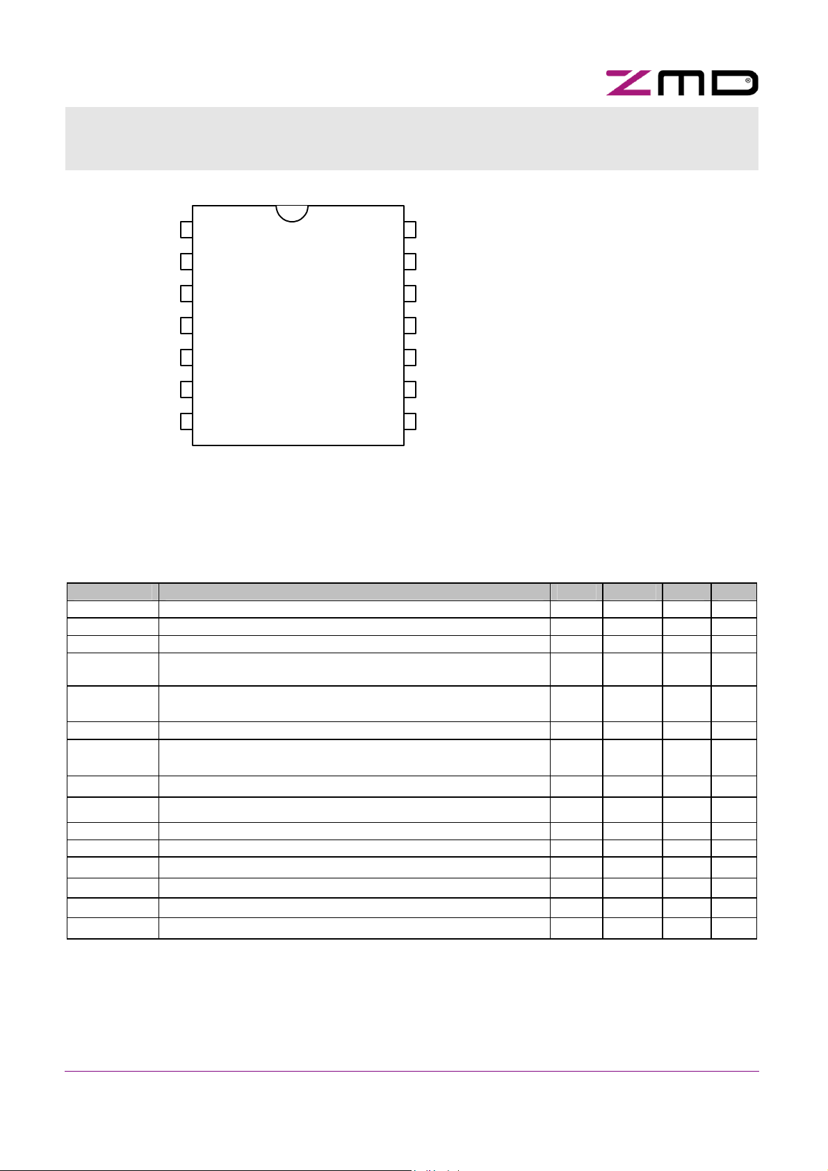
6 Pin Configuration
There is only one die used for both the 14- and 16-pin-version of the A²SI-L. In the 14-pin-version, the internal
ports FID and LED are not bonded to external pins.
ASIPOS
ASINEG
TEST1
TEST2
FID
DI2
DI3
OSC1
1
2
3
4
5
6
7
8 9
A²SI-L16
16
15
14
13
12
11
10
VIN
0V
CAP
GND
LED
DO0
DO1
OSC2
Figure 6-1: SOP16 Pin out
Rev. 2.0, Copyright © 2005, ZMD AG
All rights reserved. The material contained herein may not be reproduced, adapted, merged, translated, stored, or used without the prior written consent of the copyright owner. The
Information furnished in this publication is preliminary and subject to changes without notice.
4/22
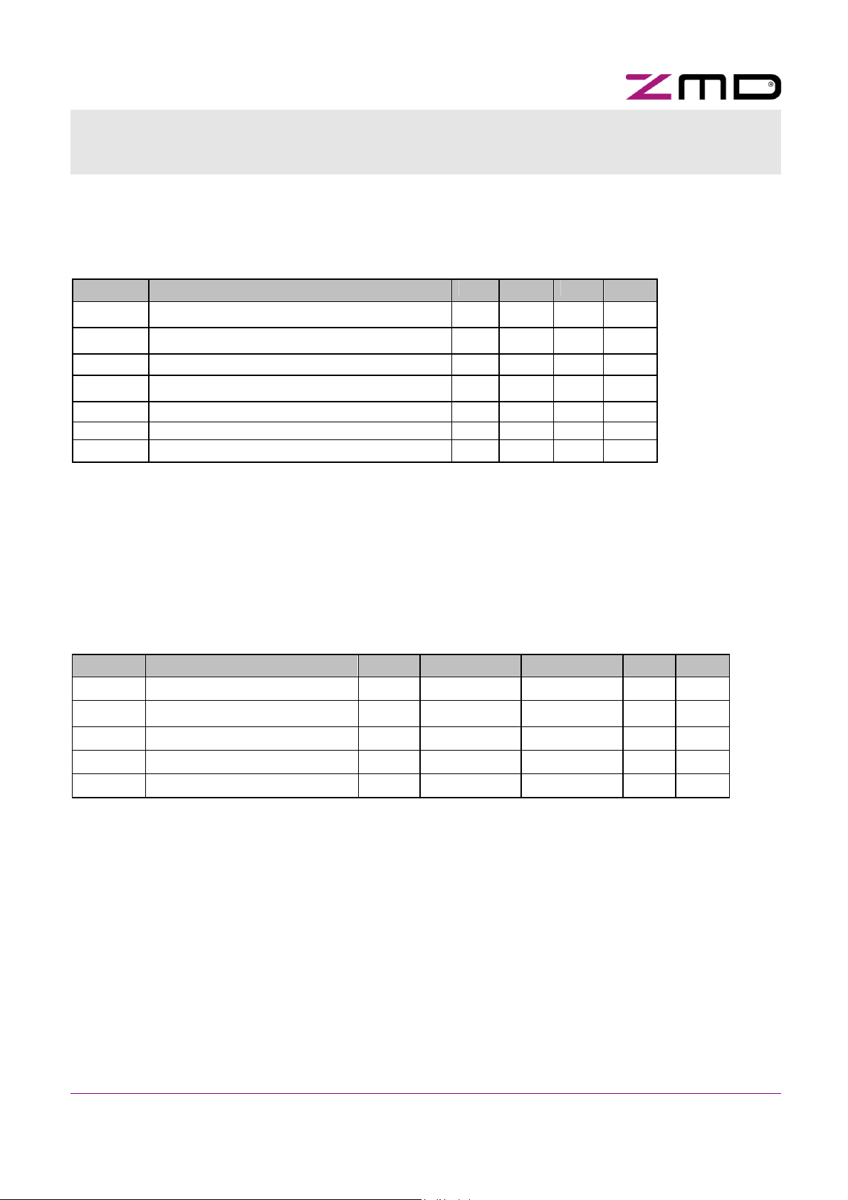
A²SI-Lite 14 / A²SI-Lite 16
Data Sheet
Low End Device AS-Interface IC
ASIPOS
ASINEG
TEST1
TEST2
DI2
DI3
OSC1
1
2
3
4
5
6
7
A²SI-L14
14
13
12
11
10
VIN
0V
CAP
GND
DO0
9
DO1
OSC2
8
Figure 6-2: SOP14 Pin out
7 Electrical Specification
7.1 Absolute Maximum Ratings (Non Operating)
Table 7-1: Absolute Maximum Ratings
Symbol Parameter min max. Unit Note
V0V ,VGND Voltage reference 0 0 V
VASIP Positive AS-i supply voltage -0.3 40 V
VASIN Negative AS-i supply voltage -0.3 20 V 1
VASIPASIN
VASIPP
VVIN Power supply input voltage -0.3 40 V
Vinputs1 Voltage at pins DI2, DI3, DO0, DO1, LED, FID -0.3 VVIN +
Vinputs2 Voltage at pins OSC1, OSC2, CAP, TEST1, TEST2 -0.3 7 V
Iin Input current into any pin except supply pins -25 25 mA
Voltage difference from ASIP to ASIN (VASIP - VASIN) -0.3 40 V 2
AS-i supply pulse voltage, voltage difference between pins
50 V 3
ASIP and ASIN (from ASIP to ASIN)
V
0.3
H Humidity non-condensing 4
VHBM1 Electrostatic discharge – human body model (HBM1) 3000 V 5
VHBM2 Electrostatic discharge – human body model (HBM2) 2000 V 6
VEDM Electrostatic discharge – equipment discharge model (EDM) 400 V 7
T
Storage temperature -55 125 °C
STG
Ptot Total power dissipation 500 mW 8
1
ASIN-pin shall be shorted to the 0V and GND pin on the PCB
2
reverse polarity protection has to be performed externally
3
pulse with =< 50us, repetition rate =< 0.5 Hz
4
defined in DIN 40040 cond. F
5
HBM1: C = 100pF charged to VHBM1 with resistor R = 1.5kOhm in series, valid for ASIP-ASIN only.
6
HBM2: C = 100pF charged to VHBM2 with resistor R = 1.5kOhm in series, valid for all pins except ASIP-ASIN
7
EDM: C = 200pF charged to VEDM with no resistor in series, valid for ASIP-ASIN only
Rev. 2.0, Copyright © 2005, ZMD AG
All rights reserved. The material contained herein may not be reproduced, adapted, merged, translated, stored, or used without the prior written consent of the copyright owner. The
Information furnished in this publication is preliminary and subject to changes without notice.
5/22
A²SI-Lite 14 / A²SI-Lite 16
Data Sheet
Low End Device AS-Interface IC
8
at max. operating temperature, the allowed total power dissipation depends on the additional thermal resistance from case to ambient and
on the operation ambient temperature.
7.2 Recommended Operating Conditions
Table 7-2: Recommended Operating Conditions
Symbol Parameter min max. Unit Note
VVIN,1 Positive supply voltage 12 31.6 V 1
VVIN,2 Positive supply voltage 20 31.6 V 2
VASIN Negative AS-i supply voltage 0 0 V 3
V0V, VGND Negative supply voltage 0 0 V
IVIN Supply current at VVIN = 30V 8.5 mA 4
ICL1 max. output sink current at pins DO0, DO1 15 mA
T
Ambient temperature range, operating range -25 85 °C
amb
1 all operations without EEPROM-write access are allowed
2 necessary for operations with EEPROM-write access only (processing of ADRA and WID1 master calls,
refer to Table 8-1)
3 ASIN shall be shorted with 0V and GND in order to ensure proper functionality of transmitter circuit.
4 fc = 16.000 MHz, no load at any pin, without reaction of the circuit, ASIN is short-circuit to 0V, VIN = 30V.
Table 7-3 describes the crystal parameter that shall be satisfied by the x-tal that is interconnected to the pins OSC1 and OSC2. Due to the
fact that the crystal parameter do not represent the entire internal and external oscillator circuit at all practical tests must indicate whether a
crystal may work in a certain application circuit (PCB) or not. Appendix A list certain types of crystals that are going to be used as reference
devices.
Table 7-3: Crystal Properties1
Symbol Parameter Nom. Min. Max. Unit Note
Fc Crystal frequency 16000 Fc – 60 ppm Fc + 60 ppm kHz
Cs Series capacitor 5 13 fF
Rs Series resistor 65 Ohm
Cp Parasitic parallel capacitor 5 pF
Cload Crystal dedicated parallel load 152 pF
1
Crystal properties according to the crystal manufacturer data sheet
2
In order to keep the influence of the crystal to the network error rate low as possible it is recommended to keep the crystal dedicated load
between 8 pF and 32 pF. The IC provides approximately a load capacity of about 10 pF to 15 pF (correct by design).
7.3 Quality Assurance
The quality of the IC will be ensured accordingly to the ZMD quality standards.
7.4 DC and AC Characteristic of all Pins and Functions
All parameters are valid for the recommended range of VASIP - VASIN and TAMB. The devices are tested within the
recommended range of V
stated. Unused input pins shall be connected to a suitable potential within the application circuit because there
are no internal pull-up/down resistors. It is recommended to connect these pins either to 0V or via resistor to
VIN.
In order to ensure a normal operation of the IC the pins TEST1 and TEST must be connected to ground
potential (GND).
Rev. 2.0, Copyright © 2005, ZMD AG
All rights reserved. The material contained herein may not be reproduced, adapted, merged, translated, stored, or used without the prior written consent of the copyright owner. The
Information furnished in this publication is preliminary and subject to changes without notice.
6/22
ASIP - VASIN, TAMB = +25°C (+ 85°C and - 25°C on sample base only) unless otherwise
A²SI-Lite 14 / A²SI-Lite 16
Data Sheet
Low End Device AS-Interface IC
7.4.1 Digital input and output Pins
Controlled by a configuration flag that is stored inside the EEPROM the data output signals can be pulse width
modulated (PWM, for information refer to chapter 8.6.2).
The functionality of the FID output port is described in chapter 8.7.
Table 7-4: Input Voltages and Currents: Pins DI2, DI3, FID, TEST1/2 1
Symbol Parameter Min Max. Unit Note
VIL Voltage range for input ”low” level 0 2.5 V
VIH Voltage range for input ”high” level 3.5 V
V
Hysteresis for switching level 0.25 V 2
HYST
IIL Current range for input ”low” level -20 -5 µA
IIH Current range for input ”high” level -10 10 µA VO = 5V
I
Current range for high voltage input 2 mA VO = 30V
IHV
1
TEST1/2 are inputs for test purposes only.
2
switching level approx. 3V, i.e. 3V +/- VHYST ; the maximum hysteresis is determined by (min.) VIH – (max) VIL
3
Valid for high voltage input pins DI2, DI3 and FID. The regular logic swing is 0 .. 5V although higher input voltages might be applied (refer
to parameter V
that is caused by the input protection circuitry (refer to parameter I
inputs1 in Table 7-1). In the case of input voltages that exceed 5V a significant higher input current will flow into the input
IHV of Table 7-4 and Figure 7-1).
V 3
VIN
5V
DIx/
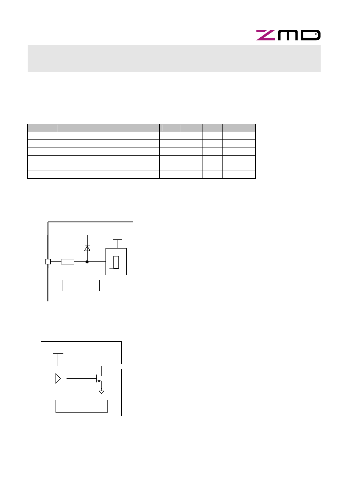
FID
A²SI-L IC
Figure 7-1: Data Input Schematic in
Principle
5V
5V
DOx
A²SI-L IC
Figure 7-2: Data Output Schematic in Principle
Rev. 2.0, Copyright © 2005, ZMD AG
All rights reserved. The material contained herein may not be reproduced, adapted, merged, translated, stored, or used without the prior written consent of the copyright owner. The
Information furnished in this publication is preliminary and subject to changes without notice.
7/22
 Loading...