

A²SI-Lite 14 / A²SI-Lite 16
Data Sheet
Low End Device AS-Interface IC
1 Features
• Fully operable in AS-interface networking
systems and capable of working in extended
networks with up to 62 slaves (V2.11)
• Dedicated IO-port structure: two data inputs, two
data outputs, no parameter port pins
• Integrated EEPROM stores relevant AS-i
information and IC configuration data (e.g. enabling/disabling of the PWM feature)
• Programmable PWM of output signals can be
used to control intensity of driven LEDs
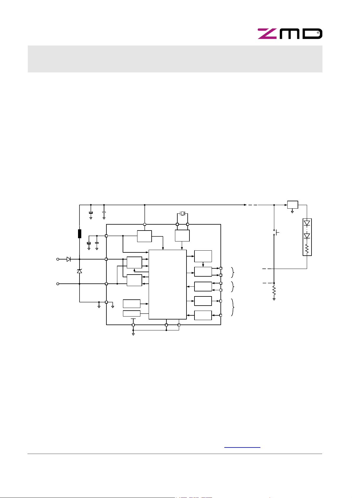
3 Block Diagram
10uF
100nF
VIN
18 mH
ASI+
ASI-
AS-i network
cable access
CAP
100nF
1uF
ASIP
ASIN
0V
5V
Receiver
Trans-
mitter
Thermal
Protection
EEPROM
GND
Power
Supply
Power on
Reset
DIGITAL
LOGIC
UART
State Machine
Ports
TEST1 TEST2
OSC1
2 Description
This integrated circuit shall be used as simplified
interface IC for key control panels, simple sensors
and small actuators based on the AS-i
specifications. The device shall be in compliance
with AS-i Specification V2.11. The IC performs
multiple interface functions.
There are two package options; the 14 pin SOP
option A²SI-Lite 14 (A²SI-L14) and the 16 pin SOP
option A²SI-Lite 16 (A²SI-L16). In contrast to the
A²SI-L14 IC the A²SI-L16 IC has two more pins; a
diagnostic LED output pin (LED pin) and a fault
indicator input pin (FID pin).
Voltage
Regulator
16MHz
Oscillator
OSC2
A²SI-L14
A²SI-L16
Pulse
Width
Modulation
Output
Stages
Input
Stages
Output
Stages
Input
Stages
DO0
DO1
DI2
DI3
LED
FID
Slave electronics
supply voltage
Two outputs, e.g.
interconnced to push
button LEDs
Two inputs, e.g.
interconnced to push
button contacts
diagnostic pins,
available at A²SIL16 version only
Switch
GND
LED-Lamp
24V
Application
Figure 3-1: Block Diagram
4 Application Support
Configuration of the chip is handled through programming of the on-chip E²PROM. ZMD provides a
special
AS-Interface Programmer Tool
(Ordering Code: 3000003356 )
to ease product evaluation and selection of different operation modes.
Further application support is available through e-mail hotline under asi@zmd.de
Rev. 2.0, Copyright © 2005, ZMD AG
All rights reserved. The material contained herein may not be reproduced, adapted, merged, translated, stored, or used without the prior written consent of the copyright owner. The
Information furnished in this publication is preliminary and subject to changes without notice.
1/22

A²SI-Lite 14 / A²SI-Lite 16
Data Sheet
Low End Device AS-Interface IC
Table of Contents Page
1 FEATURES ....................................................................................................................................................1
2 DESCRIPTION ...............................................................................................................................................1
3 BLOCK DIAGRAM ........................................................................................................................................1
4 APPLICATION SUPPORT.............................................................................................................................1
5 PIN DESCRIPTION ........................................................................................................................................4
6 PIN CONFIGURATION ..................................................................................................................................4
7 ELECTRICAL SPECIFICATION....................................................................................................................5
7.1 ABSOLUTE MAXIMUM RATINGS (NON OPERATING) ......................................................................................5
7.2 RECOMMENDED OPERATING CONDITIONS...................................................................................................6
7.3 QUALITY ASSURANCE ................................................................................................................................6
7.4 DC AND AC CHARACTERISTIC OF ALL PINS AND FUNCTIONS........................................................................6
7.4.1 Digital input and output Pins ............................................................................................................7
7.4.2 AS-i Bus Load (Pins ASIP/ASIN and Power Supply Input VIN) ......................................................8
7.4.3 Pins OSC1, OSC2 ...........................................................................................................................8
7.5 INFORMATION DATA FOR DEVELOPMENT .....................................................................................................8
8 FUNCTIONAL DESCRIPTION ....................................................................................................................10
8.1 FUNCTIONAL BLOCK DIAGRAM..................................................................................................................10
8.2 POWER SUPPLY ......................................................................................................................................10
8.3 RECEIVER ...............................................................................................................................................10
8.4 TRANSMITTER .........................................................................................................................................10
8.5 DIGITAL LOGIC.........................................................................................................................................11
8.6 DATA I/O PORTS .....................................................................................................................................12
8.6.1 Data Exchange Model....................................................................................................................12
8.6.2 PWM Function ...............................................................................................................................12
8.7 FID INPUT AND LED OUTPUT PORTS .......................................................................................................14
9 TYPICAL APPLICATION CIRCUIT OF A²SI-L ...........................................................................................15
10 PACKAGE OUTLINE AND DEVICE MARKING .....................................................................................16
11 ORDERING INFORMATION ....................................................................................................................17
12 APPLICATION SUPPORT .......................................................................................................................18
12.1 AS-INTERNATIONAL ASSOCIATION ........................................................................................................18
12.2 ZMD ...................................................................................................................................................18
12.3 ZMD APPLICATION SUPPORT PARTNERS ..............................................................................................18
13 ZMD SALES CONTACTS ........................................................................................................................18
14 ZMD DISTRIBUTION PARTNERS ..........................................................................................................19
Rev. 2.0, Copyright © 2005, ZMD AG
All rights reserved. The material contained herein may not be reproduced, adapted, merged, translated, stored, or used without the prior written consent of the copyright owner. The
Information furnished in this publication is preliminary and subject to changes without notice.
2/22

A²SI-Lite 14 / A²SI-Lite 16
Data Sheet
Low End Device AS-Interface IC
APPENDIX A: CRYSTAL PARAMETER ...............................................................................................20
A.1 PARAMETER DATA OF CRYSTAL.....................................................................................................................20
A.2 CAPACITANCE ON PCB ................................................................................................................................20
APPENDIX B: EXTERNAL COIL ...........................................................................................................21
B.1 TARGET COIL ..........................................................................................................................................21
B.2 COIL MODELING ......................................................................................................................................21
B.3 ELECTRONIC INDUCTOR ...........................................................................................................................21
APPENDIX C: EEPROM ........................................................................................................................22
List of Figures Page
Figure 3-1: Block Diagram ....................................................................................................................................1
Figure 5-1: SOIC16 Pin out ...................................................................................................................................4
Figure 5-2: SOIC14 Pin out ...................................................................................................................................5
Figure 6-1: Data Input Schematic in Principle ....................................................................................................7
Figure 6-2: Data Output Schematic in Principle .................................................................................................7
Figure 6-3: Receiver comparator threshold set-up in principle........................................................................9
Figure 6-4: Reset Behavior ...................................................................................................................................9
Figure 7-1: Functional Block Diagram...............................................................................................................10
Figure 7-2: A²SI-L IC Data Exchange master call data model .........................................................................12
Figure 7-3: PWM control .....................................................................................................................................13
Figure 7-4: PWM Output Signal Timing .............................................................................................................14
Figure 8-1: Typical Application of A²SI-L14 IC .................................................................................................15
Figure 8-2: Typical Application of A²SI-L16 IC .................................................................................................15
Figure 9-1: SOIC Package Outline Dimensions................................................................................................16
Figure 9-2: Mark Diagram of 14 Pin SOIC Version ...........................................................................................17
Figure 9-3: Mark Diagram of 16 Pin SOIC Version ...........................................................................................17
Figure A-1: Crystal oscillator equivalent circuit...............................................................................................20
Figure B-1: External Coil equivalent circuits....................................................................................................21
List of Tables Page
Table 4-1: A²SI-L14/ A²SI-L16 Pin Description ....................................................................................................4
Table 6-1: Absolute Maximum Ratings................................................................................................................5
Table 6-2: Recommended Operating Conditions ...............................................................................................6
Table 6-3: Crystal Properties
Table 6-4: Input Voltages and Currents: Pins DI2, DI3, FID, TEST1/2
Table 6-5: Output Voltages and Currents: Pins DO0, DO1, LED ......................................................................8
Table 6-6: AS-i Bus Interface Properties.............................................................................................................8
Table 6-7: Oscillator Pins......................................................................................................................................8
Table 6-8: Information Data ..................................................................................................................................8
Table 7-1: A²SI-L Master Calls and Related Slave Responses........................................................................11
Table 7-2: PWM specification of Outputs: Pins DO0, DO1..............................................................................13
Table 9-1: Package Outline Dimensions ...........................................................................................................17
Table A-1: 16 MHz crystals .................................................................................................................................20
Table A-2: Crystal models...................................................................................................................................20
Table C-1: Contents of the A²SI-L14 / A²SI-L16 EEPROM................................................................................22
1
...............................................................................................................................6
1
............................................................7
Rev. 2.0, Copyright © 2005, ZMD AG
All rights reserved. The material contained herein may not be reproduced, adapted, merged, translated, stored, or used without the prior written consent of the copyright owner. The
Information furnished in this publication is preliminary and subject to changes without notice.
3/22
A²SI-Lite 14 / A²SI-Lite 16
Data Sheet
Low End Device AS-Interface IC
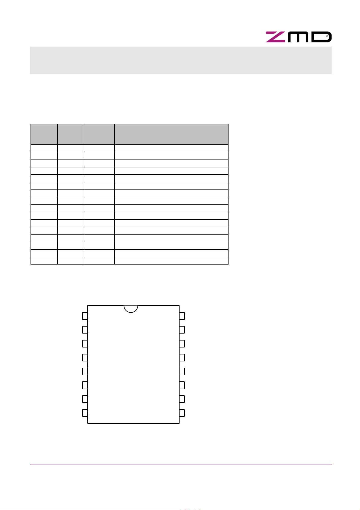
5 Pin Description
Table 5-1 shows the pin description for both the A²SI-L14 and the A²SI-L16 IC. The graphical representation
(pin-out symbols) are shown in chapter 6.
Table 5-1: A²SI-L14/ A²SI-L16 Pin Description
Pin#
SOIC16
Pin#
SOIC14
Name Description
1 1 ASIPOS positive ASI supply, high voltage supply
2 2 ASINEG negative ASI supply
3 3 TEST1 test mode input/output
4 4 TEST2 test mode input
5 FID digital input
6 5 DI2 digital input
7 6 DI3 digital input
8 7 OSC1 crystal oscillator input
9 8 OSC2 crystal oscillator output
10 9 DO1 digital output
11 10 DO0 digital output
12 LED digital output
13 11 GND digital ground
14 12 CAP regulator output
15 13 0V analog ground
16 14 VIN High voltage supply
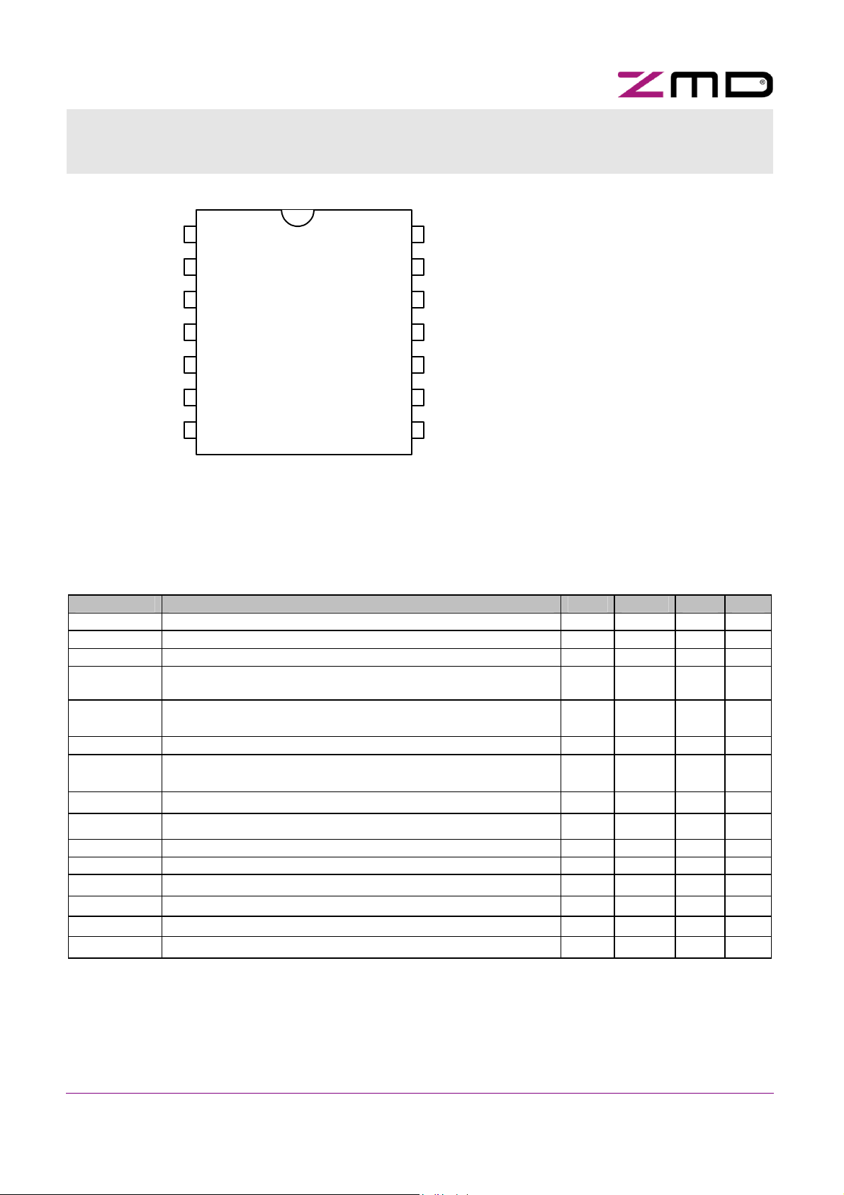
6 Pin Configuration
There is only one die used for both the 14- and 16-pin-version of the A²SI-L. In the 14-pin-version, the internal
ports FID and LED are not bonded to external pins.
ASIPOS
ASINEG
TEST1
TEST2
FID
DI2
DI3
OSC1
1
2
3
4
5
6
7
8 9
A²SI-L16
16
15
14
13
12
11
10
VIN
0V
CAP
GND
LED
DO0
DO1
OSC2
Figure 6-1: SOP16 Pin out
Rev. 2.0, Copyright © 2005, ZMD AG
All rights reserved. The material contained herein may not be reproduced, adapted, merged, translated, stored, or used without the prior written consent of the copyright owner. The
Information furnished in this publication is preliminary and subject to changes without notice.
4/22
A²SI-Lite 14 / A²SI-Lite 16
Data Sheet
Low End Device AS-Interface IC
ASIPOS
ASINEG
TEST1
TEST2
DI2
DI3
OSC1
1
2
3
4
5
6
7
A²SI-L14
14
13
12
11
10
VIN
0V
CAP
GND
DO0
9
DO1
OSC2
8
Figure 6-2: SOP14 Pin out
7 Electrical Specification
7.1 Absolute Maximum Ratings (Non Operating)
Table 7-1: Absolute Maximum Ratings
Symbol Parameter min max. Unit Note
V0V ,VGND Voltage reference 0 0 V
VASIP Positive AS-i supply voltage -0.3 40 V
VASIN Negative AS-i supply voltage -0.3 20 V 1
VASIPASIN
VASIPP
VVIN Power supply input voltage -0.3 40 V
Vinputs1 Voltage at pins DI2, DI3, DO0, DO1, LED, FID -0.3 VVIN +
Vinputs2 Voltage at pins OSC1, OSC2, CAP, TEST1, TEST2 -0.3 7 V
Iin Input current into any pin except supply pins -25 25 mA
Voltage difference from ASIP to ASIN (VASIP - VASIN) -0.3 40 V 2
AS-i supply pulse voltage, voltage difference between pins
50 V 3
ASIP and ASIN (from ASIP to ASIN)
V
0.3
H Humidity non-condensing 4
VHBM1 Electrostatic discharge – human body model (HBM1) 3000 V 5
VHBM2 Electrostatic discharge – human body model (HBM2) 2000 V 6
VEDM Electrostatic discharge – equipment discharge model (EDM) 400 V 7
T
Storage temperature -55 125 °C
STG
Ptot Total power dissipation 500 mW 8
1
ASIN-pin shall be shorted to the 0V and GND pin on the PCB
2
reverse polarity protection has to be performed externally
3
pulse with =< 50us, repetition rate =< 0.5 Hz
4
defined in DIN 40040 cond. F
5
HBM1: C = 100pF charged to VHBM1 with resistor R = 1.5kOhm in series, valid for ASIP-ASIN only.
6
HBM2: C = 100pF charged to VHBM2 with resistor R = 1.5kOhm in series, valid for all pins except ASIP-ASIN
7
EDM: C = 200pF charged to VEDM with no resistor in series, valid for ASIP-ASIN only
Rev. 2.0, Copyright © 2005, ZMD AG
All rights reserved. The material contained herein may not be reproduced, adapted, merged, translated, stored, or used without the prior written consent of the copyright owner. The
Information furnished in this publication is preliminary and subject to changes without notice.
5/22
A²SI-Lite 14 / A²SI-Lite 16
Data Sheet
Low End Device AS-Interface IC
8
at max. operating temperature, the allowed total power dissipation depends on the additional thermal resistance from case to ambient and
on the operation ambient temperature.
7.2 Recommended Operating Conditions
Table 7-2: Recommended Operating Conditions
Symbol Parameter min max. Unit Note
VVIN,1 Positive supply voltage 12 31.6 V 1
VVIN,2 Positive supply voltage 20 31.6 V 2
VASIN Negative AS-i supply voltage 0 0 V 3
V0V, VGND Negative supply voltage 0 0 V
IVIN Supply current at VVIN = 30V 8.5 mA 4
ICL1 max. output sink current at pins DO0, DO1 15 mA
T
Ambient temperature range, operating range -25 85 °C
amb
1 all operations without EEPROM-write access are allowed
2 necessary for operations with EEPROM-write access only (processing of ADRA and WID1 master calls,
refer to Table 8-1)
3 ASIN shall be shorted with 0V and GND in order to ensure proper functionality of transmitter circuit.
4 fc = 16.000 MHz, no load at any pin, without reaction of the circuit, ASIN is short-circuit to 0V, VIN = 30V.
Table 7-3 describes the crystal parameter that shall be satisfied by the x-tal that is interconnected to the pins OSC1 and OSC2. Due to the
fact that the crystal parameter do not represent the entire internal and external oscillator circuit at all practical tests must indicate whether a
crystal may work in a certain application circuit (PCB) or not. Appendix A list certain types of crystals that are going to be used as reference
devices.
Table 7-3: Crystal Properties1
Symbol Parameter Nom. Min. Max. Unit Note
Fc Crystal frequency 16000 Fc – 60 ppm Fc + 60 ppm kHz
Cs Series capacitor 5 13 fF
Rs Series resistor 65 Ohm
Cp Parasitic parallel capacitor 5 pF
Cload Crystal dedicated parallel load 152 pF
1
Crystal properties according to the crystal manufacturer data sheet
2
In order to keep the influence of the crystal to the network error rate low as possible it is recommended to keep the crystal dedicated load
between 8 pF and 32 pF. The IC provides approximately a load capacity of about 10 pF to 15 pF (correct by design).
7.3 Quality Assurance
The quality of the IC will be ensured accordingly to the ZMD quality standards.
7.4 DC and AC Characteristic of all Pins and Functions
All parameters are valid for the recommended range of VASIP - VASIN and TAMB. The devices are tested within the
recommended range of V
stated. Unused input pins shall be connected to a suitable potential within the application circuit because there
are no internal pull-up/down resistors. It is recommended to connect these pins either to 0V or via resistor to
VIN.
In order to ensure a normal operation of the IC the pins TEST1 and TEST must be connected to ground
potential (GND).
Rev. 2.0, Copyright © 2005, ZMD AG
All rights reserved. The material contained herein may not be reproduced, adapted, merged, translated, stored, or used without the prior written consent of the copyright owner. The
Information furnished in this publication is preliminary and subject to changes without notice.
6/22
ASIP - VASIN, TAMB = +25°C (+ 85°C and - 25°C on sample base only) unless otherwise
A²SI-Lite 14 / A²SI-Lite 16
Data Sheet
Low End Device AS-Interface IC
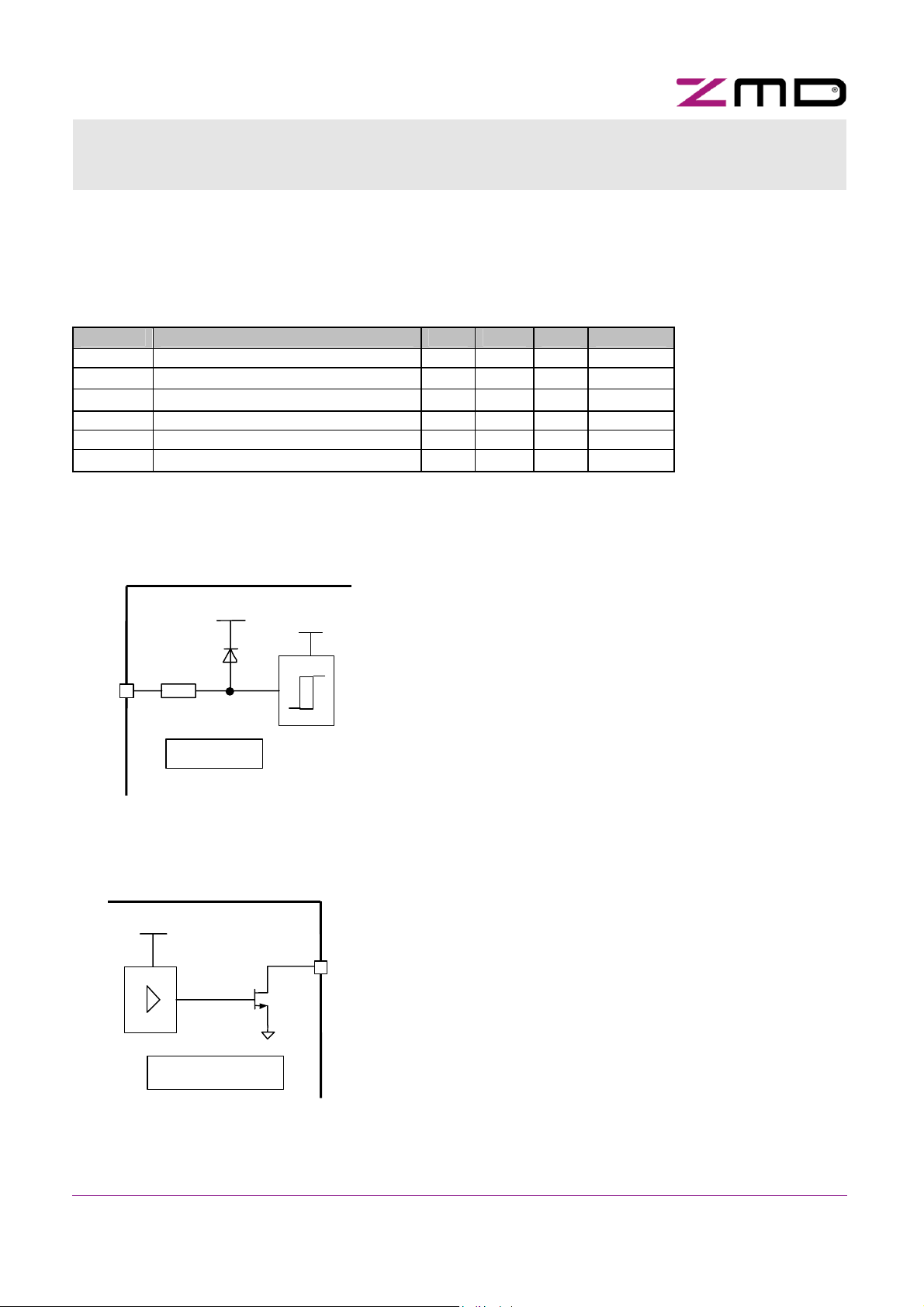
7.4.1 Digital input and output Pins
Controlled by a configuration flag that is stored inside the EEPROM the data output signals can be pulse width
modulated (PWM, for information refer to chapter 8.6.2).
The functionality of the FID output port is described in chapter 8.7.
Table 7-4: Input Voltages and Currents: Pins DI2, DI3, FID, TEST1/2 1
Symbol Parameter Min Max. Unit Note
VIL Voltage range for input ”low” level 0 2.5 V
VIH Voltage range for input ”high” level 3.5 V
V
Hysteresis for switching level 0.25 V 2
HYST
IIL Current range for input ”low” level -20 -5 µA
IIH Current range for input ”high” level -10 10 µA VO = 5V
I
Current range for high voltage input 2 mA VO = 30V
IHV
1
TEST1/2 are inputs for test purposes only.
2
switching level approx. 3V, i.e. 3V +/- VHYST ; the maximum hysteresis is determined by (min.) VIH – (max) VIL
3
Valid for high voltage input pins DI2, DI3 and FID. The regular logic swing is 0 .. 5V although higher input voltages might be applied (refer
to parameter V
that is caused by the input protection circuitry (refer to parameter I
inputs1 in Table 7-1). In the case of input voltages that exceed 5V a significant higher input current will flow into the input
IHV of Table 7-4 and Figure 7-1).
V 3
VIN
5V
DIx/
FID
A²SI-L IC
Figure 7-1: Data Input Schematic in
Principle
5V
5V
DOx
A²SI-L IC
Figure 7-2: Data Output Schematic in Principle
Rev. 2.0, Copyright © 2005, ZMD AG
All rights reserved. The material contained herein may not be reproduced, adapted, merged, translated, stored, or used without the prior written consent of the copyright owner. The
Information furnished in this publication is preliminary and subject to changes without notice.
7/22

A²SI-Lite 14 / A²SI-Lite 16
Data Sheet
Low End Device AS-Interface IC
Table 7-5: Output Voltages and Currents: Pins DO0, DO1, LED
Symbol Parameter Min Max. Unit Note
VOL Voltage range for output ”low” level 1 V IOL1 = 15mA
IOH Output leakage current -10 5 µA VOH = 30V
7.4.2 AS-i Bus Load (Pins ASIP/ASIN and Power Supply Input VIN)
The following parameters are determined with short-cut between the pins ASIN, GND, and 0V (GROUND). The
pin VIN is connected to ASIP via an external coil. A decoupling capacitor has to be interconnected between VIN
and GROUND as shown in Figure 8-1.
Table 7-6: AS-i Bus Interface Properties
Symbol Parameter min max. Unit Note
ILIN Input current limit at VIN 25 mA
VSIG Input signal voltage difference between ASIP and ASIN 3 8 VPP
ISIG Modulated output peak current from ASIP to ASIN 55 68 mAP
C
Parasitic capacitance of the external over-voltage protection diode
zener
20 pF 1
(Zener diode)
RIN Equivalent resistor of the ASIC 50 kOhm 1
CIN Equivalent capacitor of the ASIC 15 pF 1
1
The equivalent circuit of a slave has to satisfy the Complete AS-i Specification v.2.11 concerning the requirements for the extended
address range. The input impedance as function of frequency is considered as correct by design.
7.4.3 Pins OSC1, OSC2
The on chip x-tal oscillator requires a 16 MHz crystal that must be interconnected to the pins OSC1 and OSC2.
Internal capacitors make sure that no external capacitors from OSC1/OSC2 to ground are required.
Furthermore no external capacitors shall be added to OSC1 and OSC2, respectively. Due to this parasitic
capacitors shall be limited to C
to be used in A²SI-L IC application circuits.
Table 7-7: Oscillator Pins
Symbol Parameter Min max. Unit Note
COSC External parasitic capacitor at oscillator pins OSC1, OSC2 0 7 pF
VIL Input ”low” voltage 0 1.5 V 1
VIH Input ”high” voltage 3.5 5 V 2
1
for external clock applied to OSC1 only
2
for external clock applied to OSC1 only
(Table 7-7). Appendix A shows the parameter of the crystal that is supposed
OSC
7.5 Information Data for Development
Table 7-8: Information Data
Symbol Parameter min max. Unit Note
V
Falling edge of the internal 5V supply voltage that activates the
PORIF
internal power-on-reset signal
V
Rising edge of the internal voltage 5V supply voltage that causes
PORIR
the deactivation of the internal power-on-reset signal what will
cause the start of the INIT procedure
T
Chip temperature that causes an overtemp shut down 125 160
shut
Symbol Parameter min max. Unit Note
Rev. 2.0, Copyright © 2005, ZMD AG
All rights reserved. The material contained herein may not be reproduced, adapted, merged, translated, stored, or used without the prior written consent of the copyright owner. The
Information furnished in this publication is preliminary and subject to changes without notice.
8/22
3 4 V 1
2.5 3.5 V 1
o
C

A²SI-Lite 14 / A²SI-Lite 16
Data Sheet
Low End Device AS-Interface IC
V
Receiver comparator threshold level (refer to Figure 7-3) 45 50 % related to
LSIGon
amplitude of
st
1
pulse
t
reset1
T
Power-on reset pulse width 4 6 us 1
Low
1
guaranteed by design only
Reset time - either after the end bit of the sent out slave response
that is related to a received master Call Reset AS-i-Slave - or after
the IC has deactivated its power-on-reset signal
2 ms 1
"DC level"
The IC determines the
amplitude of the first
negative pulse of the
ASI telegram. This
amplitude is asserted
to be VSIG / 2.
V
LSIGon
first negative
pulse of the
V
LSIGon
= (0.45 ... 0.5) * V
V
/ 2
SIG
SIG
ASI telegram
Figure 7-3: Receiver comparator threshold set-up in principle
/ 2
V
VIN
< ca. 15V
V
CAP
V
POR1F
V
POR1R
0V
POR (low active)
t
Low
Power-on Reset will
be active if the V
drops below V
CAP
POR1F
Figure 7-4: Reset Behavior
Note: The power-on reset circuit has a threshold voltage reference. This reference matches the process
tolerance of the logic levels and is not required to be very accurate. All values depend slightly on the raise and
fall time of the supply voltage.
Rev. 2.0, Copyright © 2005, ZMD AG
All rights reserved. The material contained herein may not be reproduced, adapted, merged, translated, stored, or used without the prior written consent of the copyright owner. The
Information furnished in this publication is preliminary and subject to changes without notice.
reset will be
initalised
9/22

A²SI-Lite 14 / A²SI-Lite 16
Data Sheet
Low End Device AS-Interface IC
8 Functional Description
8.1 Functional Block Diagram
100nF
10uF
VIN
OSC1
24V
16MHz
OSC2
Power Supply
Power on
Reset
DIGITAL
State Machine
TEST1 TES T2
Oscillator
LOGIC
UART
Ports
A²SI-L
Pulse
Width
Modulation
Output
Stages
Input
Stages
Output
Stages
Input
Stages
DO0
DO1
DI2
DI3
LED
FID
Available at 16
Pin version only
ASI+
ASI-
1uF
CAP
100nF
ASIP
ASIN
5V
Receiver
Transmitter
0V
Thermal
Protection
EEPROM
GND
Figure 8-1: Functional Block Diagram
8.2 Power Supply
The power supply is derived from the AS-i line through an external reverse polarity protection diode and coil,
and provided at pin V
IN. An on-chip voltage regulator regulates the voltage at approximately 5V.
8.3 Receiver
The receiver detects the signals on the AS-i line and delivers the appropriate pulses to the digital logic. The DC
value of the input signal is removed and the AC signal is band-pass filtered. This circuit is operating on both
ASI+ and ASI- lines to take the differential nature of the signals into account. The digital output signals are
extracted from the sin
2
-shaped input pulses by a set of comparators. The maximum voltage of the first pulse
determines the threshold level for all following pulses. This maximum value is digitally filtered to guarantee
stable conditions (burst spikes have no effect). This approach combines a fast adaptation to changing signal
amplitudes with a high detection safety. The receiver delivers the positive and negative pulses to the ASIC’s
logic. The logic resets the comparators after receiving with the REC_RESET signal. When the receiver is turned
on the transmitter is turned off to reduce the power consumption.
8.4 Transmitter
The transmitter draws a modulated current between the ASI+ and ASI- pins to generate the communication
signals. The shape of the current corresponds to the integral of a sin
DAC and a high current driver. This driver must be activated before the transmission to achieve operating
conditions. A small current is required which will be ramped up slowly to avoid any false voltage pulses on the
Rev. 2.0, Copyright © 2005, ZMD AG
All rights reserved. The material contained herein may not be reproduced, adapted, merged, translated, stored, or used without the prior written consent of the copyright owner. The
Information furnished in this publication is preliminary and subject to changes without notice.
10/22
2
-function. The transmitter uses a current

A²SI-Lite 14 / A²SI-Lite 16
Data Sheet
Low End Device AS-Interface IC
AS-i line. The amount of circuitry between the ASI+ and ASI- pins is minimized to allow high impedance values.
When the transmitter is turned on the receiver is turned off to reduce the power consumption.
8.5 Digital Logic
The digital logic block analyses the received signal, controls the reaction of the slave, transmits the slave
response and switches the output ports.
Essential parts of the digital logic are as follows:
• The UART performs a syntactical analysis of the incoming master signal and executes the Manchester-
coding of the outgoing slave answer.
• The STATE MACHINE controls the overall behavior of the slave. Depending on the configuration data
provided by the EEPROM and the logic levels at the digital input ports it computes the contents of the slave
answer where required. Table 8-1 lists all master calls that will be decoded by the A²SI-L IC. Moreover, the
logic state of the digital output ports is controlled by the
contain more detailed descriptions of the digital I/O-ports.
• The EEPROM stores the non-volatile data of the A²SI-L circuit. A specification of the EEPROM contents is
given in Table C-1 on page 22. The meaning of some configuration flags are explained below and in
Chapter 8.6, respectively.
By setting the
Program_Mode_Disable flag (refer to Table C-1), the manufacturers of AS-i slave components
may protect the entire firmware area – addresses 0x8 up to 0xC – against accidental overwriting.
Watchdog_Active flag enables the internal communication watchdog. Once the communication was
The
activated, it will trigger an unconditional reset as soon as it detects a data communication pause longer than
40ms. It should be noted that only the reception of a
master call can reset the watchdog.
STATE MACHINE as well. Chapters 8.6 and 8.7
Write Parameter (WPAR) or Data Exchange (DEXG)
Table 8-1: A²SI-L Master Calls and Related Slave Responses
Instructi on MNE ST CB A4 A3 A2 A1 A0 I4 I3 I2 I1 I0 PB EB SB I3 I2 I1 I0 PB EB
Data Exchange
Write Parameter
Address Assignment
Write Extented ID
Code_1
Delete Address
Reset Slave
Read IO
Configuration
Read ID Code
Read ID Code_1
Read ID Code_2
Read Status
Broadcast (Reset)
Enter Program Mode
DEXG 0 0 A4 A3 A2 A1 A0 0
WPAR 0 0 A4 A3 A2 A1 A0 1
ADRA 0 0 0 0 0 0 0 A4 A3 A2 A1 A0 PB 1 0 0 1 1 0 PB 1
WID1 01000000ID3ID2ID1ID0PB1 00000PB1
DELA 0 1 A4 A3 A2 A1 A0 0 0 Sel 0 0 0 PB 1 0 0 0 0 0 PB 1
RES 0 1 A4A3A2A1A0 1
RDIO 0 1 A4A3A2A1A0 1
RDID 0 1 A4A3A2A1A0 1
RID1 0 1 A4 A3 A2 A1 A0 1
RID2 0 1 A4 A3 A2 A1 A0 1
RDST 0 1 A4A3A2A1A0 1
BR01 0 1 1 1 1 1 1 1 0 1 0 1 PB 1 --- no slave response ---
PRGM 0 1 0 0 0 0 0 1 1 1 0 1 PB 1 --- no slave response ---
Master Request Slave Response
D3
D2 D1 D0 PB 1 0
~Sel
P3
P2 P1 P0 PB 1 0 P3 I3 P2 I2 P1 I1 P0 I0 PB 1
~Sel
1
100PB1 00110PB1
~Sel
0
0 0 0 PB 1 0 IO3 IO2 IO1 IO0 PB 1
Sel
0
0 0 1 PB 1 0 ID3 ID2 ID1 ID0 PB 1
Sel
0
0 1 0 PB 1 0 ID3 ID2 ID1 ID0 PB 1
Sel
0
0 1 1 PB 1 0 ID3 ID2 ID1 ID0 PB 1
Sel
1
1 1 0 PB 1 0 S3 S2 S1 S0 PB 1
~Sel
0 E30 E2D1 E1D0
Notes:
E0
PB 1
Rev. 2.0, Copyright © 2005, ZMD AG
All rights reserved. The material contained herein may not be reproduced, adapted, merged, translated, stored, or used without the prior written consent of the copyright owner. The
Information furnished in this publication is preliminary and subject to changes without notice.
11/22

A²SI-Lite 14 / A²SI-Lite 16
Data Sheet
Low End Device AS-Interface IC
• In extended address mode the "Select Bit" defines whether the A- Slave or B- Slave is being addressed.
• The Enter Program Mode master call is intended for factory programming of the IC only. In order to achieve
EEPROM firmware protection and in order to satisfy the AS-interface Complete Specification the call
Program Mode must be deactivated by setting the Program_Mode_Disable flag before shipment of the
slave.
8.6 Data I/O Ports
8.6.1 Data Exchange Model
All Data_Out and Data_In signals are directly connected to the respective port (refer to Figure 8-2). The A²SI-L
IC has only two data output pins (DO0 and DO1). Therefore the information bits I3 and I2 of the master call are
not transferred to the
lower order information bit (I1 and I0) of the slave response are set to “0” if the IC answers a
master telegram.
If the EEPROM flag
the circuitry for NPN-inputs.
A²SI-L data outputs. Since the A²SI-L IC has only two data input pins (DI2 and DI3) both
Data Exchange
Invert_Data_In (refer to Table C-1) is set, all input data is inverted. This feature will simplify
Enter
3
2
1
I
n.c.
I
n.c.
I
I
0
0
I3
I2
I1
Master
I0
0
A²SI-L IC
Figure 8-2: A²SI-L IC Data Exchange master call data model
The data input pins (DI2 and DI3) are sampled in a time frame that starts not earlier as the point in time of the
end bit of the related
corresponding slave response. In the same time frame the data output pins will change their state if
appropriated.
8.6.2 PWM Function
The regular function of the data pins DO0 and DO1 is to send out the corresponding master telegram data of
the call
addition to that the
that are interconnected to DO0 and/or DO1, respectively. The PWM function may be enabled by the EEPROM
flag
Data Exchange (DEXG, refer to Table 7-5). DO0 corresponds to I0 and DO1 corresponds to I1. In
PWM_enable (refer to Table C-1).
Data Exchange master call and ends at least at the end of the start bit of the
A²SI-L IC performs a PWM function which is dedicated for the brightness control of LEDs
data ports
DI3
DI2
DO1
DO0
Rev. 2.0, Copyright © 2005, ZMD AG
All rights reserved. The material contained herein may not be reproduced, adapted, merged, translated, stored, or used without the prior written consent of the copyright owner. The
Information furnished in this publication is preliminary and subject to changes without notice.
12/22

A²SI-Lite 14 / A²SI-Lite 16
Data Sheet
Low End Device AS-Interface IC
Table 8-2: PWM specification of Outputs: Pins DO0, DO1
LED
“Write Parameter” command from Master 1 Intensity of
P2 P1 P0
PWM
Frequency 2
Pulse duty ratio
3
ton / tPWM
1 / tPWM
100.00% Select DO0 or
1 1 DC (default) 16/16
DO1
50.00% Select DO0 or
0 1 125Hz 8/16
DO1
25.00% Select DO0 or
1 0 125Hz 4/16
DO1
12.50% Select DO0 or
1
The write parameter call is used to control the intensity of LEDs that are interconnect to the data output pins.
2
Correct by design
3
Pulse/duty ratio is defined as the quotient ton / tPWM (refer to Table 8-2)
DO1
0 0 125Hz 2/16
Provided that a lit LED is caused by a logic low level output signal of the related data pin brightness of the LED
can be controlled by the master call
Write Parameter (WPAR, refer to Table 8-1) as shown in Figure 8-3. After a
Write Parameter call has been received the pulse duty ratio will be effective after the slave response has been
sent. The default duty pause ration is 100% which is set after the initialization phase of the IC automatically.
Figure 8-3 shows the telegram structure of the
Write Parameter call. and the related slave response data.
0 A0A1A2A3A40 1 1PBP0P1P2
ST SB
Slave address
Master Telegram
~Sel
P3
EB
Intensity
data
Output select
1: DO0
0: DO1
~Sel
0 1PBP0P1P2
P3
ST
Intensity data
Slave Response
sent back
from the slave
to the master
Figure 8-3: PWM control
Rev. 2.0, Copyright © 2005, ZMD AG
All rights reserved. The material contained herein may not be reproduced, adapted, merged, translated, stored, or used without the prior written consent of the copyright owner. The
Information furnished in this publication is preliminary and subject to changes without notice.
13/22

A²SI-Lite 14 / A²SI-Lite 16
Data Sheet
Low End Device AS-Interface IC
LED on
logic
low
level
LED off
logic
high
level
output driver DO0, DO1
V
il
time
ton
t
PWM
Figure 8-4: PWM Output Signal Timing
8.7 FID Input and LED Output Ports
The fault indication input FID is a digital input that is dedicated for a periphery fault messaging signal (for
electrical properties refer to Table 7-4 on page 7). The S1 status bit is equivalent to the FID input signal. An FID
transition will occur at S1 with a certain delay due to a synchronizer circuit which is put in between.
In case of the 14 pin IC version the FID input is not available. The manufacturer (ZMD) will disable this function
by setting the EEPROM flag
logic low input signal at an enabled FID pin. Therefore the status bit S1 is always cleared if an IC is having a
disabled FID pin.
The LED output port is used as a status indicator. An active FID (logic high) signal causes a flashing status
LED (frequency approx. 2Hz). Otherwise, if FID is not active (logic low) the status LED operation depends on
the communication status of the
exchange allowed), a steady-on LED shall indicate that the communication is off.
:
Notes
• An active FID has priority and will cause a flashing LED even if the Data_Exchange_Disable flag is set.
• If the FID pin is disabled (EEPROM flag FID_Disable set), the LED output is always set to logic high state.
FID_Disable (refer to Table C-1). A disabled FID pin function is equivalent to a
A²SI-L device. If the internal Data_Exchange_Disable flag is set (no data
Rev. 2.0, Copyright © 2005, ZMD AG
All rights reserved. The material contained herein may not be reproduced, adapted, merged, translated, stored, or used without the prior written consent of the copyright owner. The
Information furnished in this publication is preliminary and subject to changes without notice.
14/22

A²SI-Lite 14 / A²SI-Lite 16
Data Sheet
Low End Device AS-Interface IC
9 Typical application circuit of A²SI-L
ASI+
ASI-
VIN DI2
OSC1
OSC2
ASIP
ASIN
CAP
0V
GND
A²SI-L14
DI3
DO0
DO1
TEST1
TEST2
Switch
Voltage
regulator
+24V
LED lamp
Figure 9-1: Typical Application of A²SI-L14 IC
The pins ASIN, 0V and GND must be connected on the PCB.
+24V
A²SI-L16
DI2
DI3
DO0
DO1
FID
LED
TEST1
TEST2
Red
(fault in-
dication)
DI2
DI3
DO0
DO1
FAULT_IN
Green
ASI+
ASI-
VIN
OSC1
OSC2
ASIP
ASIN
CAP
0V
GND
Figure 9-2: Typical Application of A²SI-L16 IC
Rev. 2.0, Copyright © 2005, ZMD AG
All rights reserved. The material contained herein may not be reproduced, adapted, merged, translated, stored, or used without the prior written consent of the copyright owner. The
Information furnished in this publication is preliminary and subject to changes without notice.
15/22

A²SI-Lite 14 / A²SI-Lite 16
Data Sheet
Low End Device AS-Interface IC
10 Package Outline and Device Marking
The IC is available in a 14 or 16 pin SOIC-package (Figure 10-1). It has the dimensions as shown in Table 10-1.
Figure 10-2 and Figure 10-3 indicate the device marking.
Figure 10-1: SOIC Package Outline Dimensions
Rev. 2.0, Copyright © 2005, ZMD AG
All rights reserved. The material contained herein may not be reproduced, adapted, merged, translated, stored, or used without the prior written consent of the copyright owner. The
Information furnished in this publication is preliminary and subject to changes without notice.
16/22

A²SI-Lite 14 / A²SI-Lite 16
Data Sheet
Low End Device AS-Interface IC
Table 10-1: Package Outline Dimensions
A A1 B C e D E L H h alpha
SOIC 14 Inches
Min. 0.061 0.004 0.0138 0.0075 0.337 0.150 0.016 0.230 0.010 0°
Max. 0.068 0.0098 0.0192 0.0098
SOIC 16 Inches
Min. 0.061 0.004 0.0138 0.0075 0.386 0.150 0.016 0.230 0.010 0°
Max. 0.068 0.0098 0.0192 0.0098
0.050
Typ.
0.344 0.157 0.035 0.244 0.016 8°
0.050
Typ.
0.393 0.157 0.035 0.244 0.016 8°
A²SI-L14
ZMD
B
- YYWWLZZD
Pin 1 mark
A²SI-L14: Product Name
ZMD: Manufacturer
B: Revision Code
YYWW: Year / Workweek (Datecode)
L: Assembly Location
ZZD: Traceability and Status Code
Figure 10-2: Mark Diagram of 14 Pin SOIC Version
11 Ordering Information
Ordering Code Description Operating
A2SI-L14-ST
A2SI-L14-SR
A2SI-L16-ST
A2SI-L16-SR
14 pin version -25°C to 85°C SOP14 (150 mil) Tubes
14 pin version -25°C to 85°C SOP14 (150 mil) Tape-and-Reel
16 pin version
with FID / LED pin
16 pin version -25°C to 85°C SOP16 (150 mil) Tape-and-Reel
Pin 1 mark
Figure 10-3: Mark Diagram of 16 Pin SOIC Version
A²SI-L16
B
-
YYWWLZZD
A²SI-L16 : Product Name
ZMD: Manufacturer
B: Revision Code
YYWW: Year / Workweek (Datecode)
L: Assembly Location
ZZD: Traceability and Status Code
ZMD
Package Type Shipping Form
Temperature
Range
(55 parts/tube)
(2500 parts/reel)
-25°C to 85°C SOP16 (150 mil) Tubes
(55 parts/tube)
Rev. 2.0, Copyright © 2005, ZMD AG
All rights reserved. The material contained herein may not be reproduced, adapted, merged, translated, stored, or used without the prior written consent of the copyright owner. The
Information furnished in this publication is preliminary and subject to changes without notice.
17/22

A²SI-Lite 14 / A²SI-Lite 16
Data Sheet
Low End Device AS-Interface IC
with FID / LED pin (2500 parts/reel)
12 Application Support
12.1 AS-International Association
Documentation and promotional materials as well as detailed technical specifications regarding the AS-Interface
Bus Standard are available from:
AS-International Association
Contact - Rolf Becker
Zum Taubengarten 52
D-63571 Gelnhausen
PO Box 1103 Zip (63551)
Tel: +49 6051 47 32 12
Fax: +49 6051 4732 82
Email: as-interface@t-online.de
http://www.as-interface.net
Refer to the Association’s website hereabove for contact info on different local AS-Interface associations which
provide local support within Europe, in the US and in Japan.
12.2 ZMD
A²SI-L14 / A²SI-L16 device related application support requests can be addressed to asi@zmd.de
12.3 ZMD Application Support Partners
ZMD
Application
Support
Partners:
Bihl+Wiedemann
Flosswoerthstrasse 41
D-68199 Mannheim, Germany
Tel.: +49(0) 621 3 3996 0
Fax: +49(0) 621 3 3922 39
Email: mail@bihl-wiedemann.de
http://www.bihl-wiedemann.de
ICS Industrial Communication
Solutions GmbH
Hopfenstraße 1
D-88069 Tettnang, Germany
Tel: +49 (0) 7542 98 04 50
Fax: +49 (0) 7542 97 88 650
e-mail: info@ics-gmbh.com
http://www.ics-gmbh.com
13 ZMD Sales Contacts
For further
information:
ZMD AG
Grenzstrasse 28
01109 Dresden, Germany
Tel.: +49 (0)351.8822.366
Fax: +49 (0)351.8822.337
sales@zmd.de
ZMD America Inc.
201 Old Country Road, Suite 204
Melville, NY 11747
Tel.: (631) 549-2666
Fax: (631) 549-2882
sensors@zmda.com
Rev. 2.0, Copyright © 2005, ZMD AG
All rights reserved. The material contained herein may not be reproduced, adapted, merged, translated, stored, or used without the prior written consent of the copyright owner. The
Information furnished in this publication is preliminary and subject to changes without notice.
18/22

A²SI-Lite 14 / A²SI-Lite 16
Data Sheet
Low End Device AS-Interface IC
14 ZMD Distribution Partners
Germany
WBC GmbH
Im Technologiepark 2-8
D-85586 Poing
Phone: +49 8121 775 155
Fax: +49 8121 775 592
E-mail: juergen.dudda@wbc-europe.com
France
WBC
12C, rue du 35ième Régiment d'Aviation
F- 69500 Bron
Phone: +33(0) 4 72 14 84 06
Fax: +33 (0) 4 72 14 10 03
E-mail: franck.chapuis@wbc-europe.com
Austria
WBC GmbH
Diefenbachgasse 35/II/3.OG
A-1150 Wien
Phone: +43 1 89199 43,
Fax: +43 1 89199 50
E-mail: m.schania@wbc-europe.com
Products sold by ZMD are covered exclusively by the warranty, patent indemnification and other provisions appearing in ZMD standard "Terms of Sale". ZMD
makes no warranty (express, statutory, implied and/or by description), including without limitation any warranties of merchantability and/or fitness for a particular
purpose, regarding the information set forth in the Materials pertaining to ZMD products, or regarding the freedom of any products described in the Materials from
patent and/or other infringement. ZMD reserves the right to discontinue production and change specifications and prices of its products at any time and without
notice. ZMD products are intended for use in commercial applications. Applications requiring extended temperature range, unusual environmental requirements,
or high reliability applications, such as military, medical life-support or life-sustaining equipment, are specifically not recommended without additional mutually
agreed upon processing by ZMD for such applications.
ZMD reserves the right to change the detail specifications as may be required to permit improvements in the design of its products.
Northern Europe
WBC-Nordic GmbH
Anelystparken 31c,
DK-8381 Tilst
Phone: +45 8745 5858
Fax: +45 8745 5850
E-mail: claus.mortensen@wbc-europe.com
Netherlands
WBC
Smederijstraat 1B
NL-4814 Breda
Phone: +31 (0)765 30 57 -58
Fax: +31 (0) 765 305759
E-mail: W.Althuijzen@wbc-europe.com
Poland
WBC Sp. z o.o.
Wlodkowica 21
50-072 Wroclaw POLAND
Phone: +48 (0) 71 788 80 11
Fax: +48 (0) 71 788 80 13
E-mail: l.kaczmarski@wbc-europe.com
UK
WBC GmbH
Suite 7, Challenge House,
Sherwood Drive
Bletchley, Milton Keynes, MK3 6DP
Phone: +44 (0)1908 27 93 00
Fax: +44 (0) 7887 926 402
E-mail: kevin.doyle@wbc-europe.com
Itally
WBC, Manuel Nardiello
v. Frova, 34
I-20092 Cinisello Balsamo (MI)
Phone: +39-02618704.321
Fax +39-0261298226
E-mail: m.nardiello@wbc-europe.com
Russia
WBC GmbH
Korovinskoye Chaussee 10, Building 2
RUS-127486 Moscow
Tel.: +7 (095) 937 87 08
Fax: +7 (095) 937 21 66
E-mail: sergey.zabolotskiy@wbc-europe.com
Rev. 2.0, Copyright © 2005, ZMD AG
All rights reserved. The material contained herein may not be reproduced, adapted, merged, translated, stored, or used without the prior written consent of the copyright owner. The
Information furnished in this publication is preliminary and subject to changes without notice.
19/22

A²SI-Lite 14 / A²SI-Lite 16
Data Sheet
Low End Device AS-Interface IC
Appendix A: Crystal Parameter
A.1 Parameter data of Crystal
Different crystals types are described in Table A-1. The models of those crystals are described in Table A-2.
Table A-1: 16 MHz crystals
Symbol Model Maker Size
Operating Temperature Range (oC)
W* D* H (mm)
A LIM-T-16.000 Kyusyu Dentsu Co. 7.5*5.0*1.2 -25 … +85
B LAP-16.000 Kyusyu Dentsu Co. 6.0*3.5*1.2 -25 … +85
C SXN-A 16 MHz Nippon Industries 6.0*3.5*1.2 -40 … +85
D SXH-A 16 MHz Nippon Industries 7.5*5.0*1.0 -40 … +85
E DSX630G Daishinku corp. 6.0*3.5*1.2 -25 … +85
Table A-2: Crystal models
L1 (mH) C1 (fF) R1 (Ohm) C0 (pF) CL (pF) Symbol
Min. Typ. Max. Min. Typ. Max. Min. Typ. Max. Min. Typ. Max. Min. Typ. Max.
A
B
C
D
E
6.7 7.9 9.1 9.0 10.6 12.2 - - 60.0 2.4 2.9 3.3 12.0 16.0 20.0
7.9 9.3 10.7 9.0 10.6 12.2 - - 60.0 2.4 2.9 3.3 12.0 16.0 20.0
7.9 9.3 10.7 9.0 10.6 12.2 - 10.0 60.0 2.4 2.9 3.3 8.0 - 32.0
6.7 7.9 9.1 9.0 10.6 12.2 - 10.0 60.0 2.4 2.9 3.3 8.0 - 32.0
14.1 16.6 19.1 5.1 6.0 6.9 10.0 50.0 - 1.8 2.1 2.4 12.0 - 20.0
Note: A crystal is fabricated for a dedicated load capacitor. This load capacitor CL is equivalent to the sum of
CL’ (internal oscillator circuit capacitor) and the parasitic capacitor CP (capacity that is caused by the PCB,
e.g. by copper areas and wires on the PCB).
Figure A-1 shows an equivalent circuit of the crystal oscillator that should illustrate the modeling method.
A.2 Capacitance on PCB
R1
C0 CP -R
C1
L1
crystal parasitics oscillator
CL'
Figure A-1: Crystal oscillator equivalent circuit
Rev. 2.0, Copyright © 2005, ZMD AG
All rights reserved. The material contained herein may not be reproduced, adapted, merged, translated, stored, or used without the prior written consent of the copyright owner. The
Information furnished in this publication is preliminary and subject to changes without notice.
20/22

A²SI-Lite 14 / A²SI-Lite 16
Data Sheet
Low End Device AS-Interface IC
Appendix B: External Coil
B.1 Target Coil
In order to satisfy the Complete Specification AS-interface an application circuit has to achieve a certain input
impedance. Besides the A²SI-L IC properties the applied external coil will have an significant influence.
Therefore a suitable coil shall be recommended. During the product development period recommended data
of this coil have to be worked out. The following coil is considered as target component and shall be applied
(between ASIP and VIN, refer to Figure 9-1 and Figure 9-2, respectively) as long no other recommendation
has been made:
Coil No, SD75-183k
Core No, M5D DR7.8*5.0 DIM
Maker EASY MAGNET Corp. http://www.easymagnet.com.tw
Inductance: 18mH +-10% (f=1kHz Ambient Temperature : 20'C DC Bias 0A)
DC resistance : Max 72.0 ohm ( Ambient Temperature :20'C DC Bias 0A)
B.2 Coil Modeling
R' L' C'
AC circuit DC circuit
Figure B-1: External Coil equivalent circuits
Figure B-1 shows the model parameters that will be used in order to recommend suitable external coils. Until
the end of the development process the following parameters have shall be recommended by ZMD:
L' : Real value of Inductance
C' : Parasitic capacitor
R' : AC Resistance
Rdc : DC Resistance
Measurement frequency : 50k...300kHz C' R' L'
Rdc
B.3 Electronic Inductor
ZMD provides an optional application (
inductor* to replace a mechanical coil with some inexpensive electronic parts. This solution save costs,
board space and will be more resistant against mechanical vibrations. This inductor provides a supply
current up to 90mA to Vin and the connected circuit, respectively
see separate application note) for a bipolar (GND free) electronic
.
ZMD AG provides a license to ZMD AS-Interface IC customers free of charge.
patent pending
*
Rev. 2.0, Copyright © 2005, ZMD AG
All rights reserved. The material contained herein may not be reproduced, adapted, merged, translated, stored, or used without the prior written consent of the copyright owner. The
Information furnished in this publication is preliminary and subject to changes without notice.
21/22

A²SI-Lite 14 / A²SI-Lite 16
Data Sheet
Low End Device AS-Interface IC
For further information, please contact:
ZMD AG
BUS-Interface IC’s
Grenzstrasse 28
01109 Dresden,Germany
asi@zmd.de
Appendix C: EEPROM
Table C-1: Contents of the A²SI-L14 / A²SI-L16 EEPROM
EEPROM
Address
0x0 0 ... 3 A0 ... A3 Slave Address low nibble
0x1 0 A4 Slave Address high nibble
0x1 1 ... 3 (not useable) none
0x2 0 ... 3 ID1_0 ... ID1_3 ID code extension 1
0x3 0 ... 3 Not implemented - do not access
0x4 ... 0x7 0 ... 3 Not implemented - do not access
Bit
Position
EEPROM Cell Content
EEPROM Register
Content
0x8 0 ... 3 ID_0 ... ID_3 ID code
0x9 0 ... 3 ID2_0 ... ID2_3 ID code extension 2
0xA 0 ... 3 IO_0 ... IO_3 IO code
0xB 0 PWM_enable Configuration Flags
0xB 1 PWM_32k_mode
0xB 2 Reserved
0xB 3 Reserved
0xC 0 FID_Disable Configuration Flags
0xC 1 Program_Mode_Disable
0xC 2 Watchdog_Active
0xC 3 Invert_Data_In
0xD 0 ... 3 Not implemented - do not access
0xE 0 ... 3 Trimm Information, do not access
0xF 0 ... 3 Trimm Information, do not access
Rev. 2.0, Copyright © 2005, ZMD AG
All rights reserved. The material contained herein may not be reproduced, adapted, merged, translated, stored, or used without the prior written consent of the copyright owner. The
Information furnished in this publication is preliminary and subject to changes without notice.
22/22
 Loading...