


Zilog
FEATURES
PRELIMINARY
PRELIMINARY
CUSTOMER PROCUREMENT SPECIFICATION
Z90349/348
DIGITAL TELEVISION CONTROLLER
IN-CIRCUIT EMULATOR (ICE) DEVICE
Z90349/Z90348
■ Part ROM RAM Speed
Number (Word) (Word) (MHz)
Z90349 0 1K 12
Z90348 0 1K 12
■ 144-Pin Grid Array (PGA) Package (Z90349)
100-Pin Quad Flat Pack (QFP) Package (Z90348)
■ 4.5- to 5.5-Volt Operating Range
■ Z89C00 RISC Processor Core
■ 0°C to +70°C Temperature Range
GENERAL DESCRIPTION
The Z90349 and Z90348 are ROMless versions of the
Z89300 family of Zilog's Digital Television Controllers
designed for use in emulators and development boards to
provide complete audio and video control of television
receivers, video recorders, and advanced on-screen
display facilities.
The powerful Z89C00 RISC processor core allows users to
control on-board peripheral functions and registers using
the standard processor instruction set.
In closed caption mode, text can be decoded directly from
the composite video signal and displayed on the screen
with assistance from the processor's digital signal
processing capabilities. The character representation in
this mode allows for a simple attribute control through the
insertion of control characters.
The character control mode provides access to the full set
of attribute controls. The modification of attributes is allowed
on a character-by-character basis. The insertion of control
characters permits direction of other character attributes.
Display attributes, including underlining, italics, blinking,
eight foreground/background colors, character position
offset delay, and background transparency, are made
possible through a fully customized 512 character set.
■ Direct Closed Caption Decoding
■ TV Tuner Serial Interface
■ Customized Character Set
■ Character Control Mode
■ Directly Controlled Receiver Functions
■ V-Chip Decode
Serial interfacing with the television tuner is provided
through the tuner serial port. Digital channel tuning
adjustments may be accessed through the industrystandard I2C port.
Additional hardware provides the capability to display two
to three times normal size characters. The smoothing logic
contained in the on-screen display circuit improves the
appearance of larger fonts. Special circuitry can be
activated to improve the visibility of text by adding a rightsided shadow effect to the characters.
Receiver functions such as color and volume can be
directly controlled by six 8-bit pulse width modulated
ports.
Notes:
All Signals with a preceding front slash, "/", are active Low, e.g.:
B//W (WORD is active Low); /B/W (BYTE is active Low, only).
Power connections follow conventional descriptions below:
Connection Circuit Device
Power V
Ground GND V
CC
V
DD
SS
CP97TEL2600
1
Zilog
PRELIMINARY
GENERAL DESCRIPTION (Continued)
Z90349/Z90348
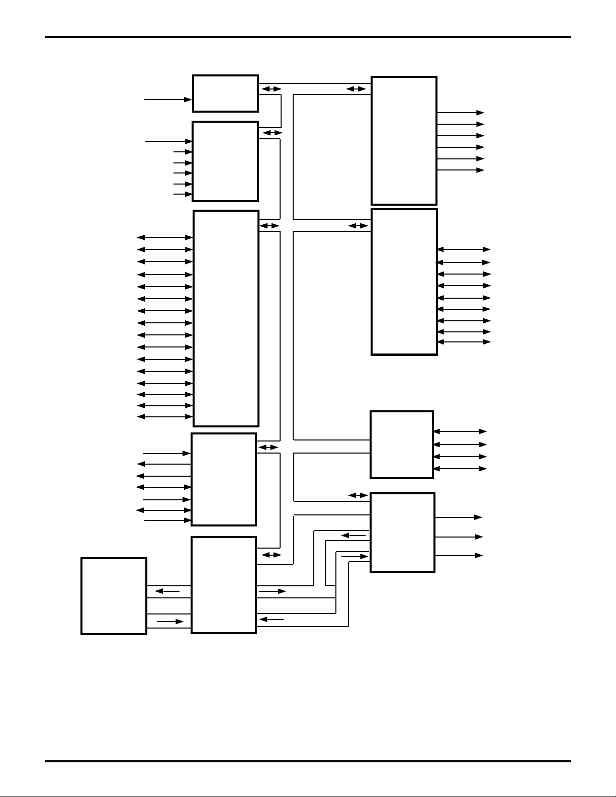
CVI
PWM6
Port 17
Port 00
Port 05
Port 04
Capture
IRIN
ADC
ADC0
ADC1
ADC2
ADC3
ADC4
ADC5
Port 0
Port 00
Port 01
Port 02
Port 03
Port 04
Port 05
Port 06
Port 07
Port 08
Port 09
Port 0A
Port 0B
Port 0C
Port 0D
Port 0E
Port 0F
Control
XTAL1
XTAL2
LPF
HSYNC
HSYNC2
VSYNC
/Reset
Register Addr/Data
PWM
PWM1
PWM2
PWM3
PWM4
PWM5
PWM6
Port1
Port 10
Port 11
Port 12
Port 13
Port 14
Port 15
Port 16
Port 17
Port 18
I2C
SCL/MSCL2
SCD/MSCD2
MSCL1
MSCD1
OSD
V1(R)
Port 01/11
Port 02/12
CPU
V2(G)
V3(B)
RAM
1K x 16
Address
Addr
Data
Data
Functional Block Diagram
2
CP97TEL2600
Zilog
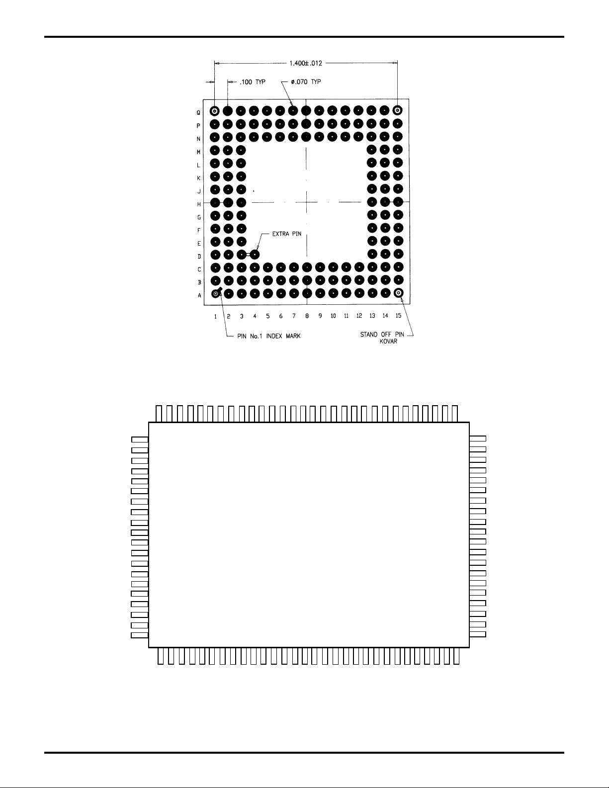
PIN DESCRIPTION
PRELIMINARY
Z90349/Z90348
100
144-Pin PGA Configuration
1
Z90348
76
75
25
26
50
51
CP97TEL2600
100-Pin QFP Configuration
3

Zilog
PRELIMINARY
PIN DESCRIPTION (Continued)
Z90349/Z90348 Pin Identification Table
Number Pin Name 144-Pin 100-Pin
1 P03 D3 52
2 P02/I2CSSC C2 53
3V
CC
4 gnd D2
5 address12 E3 54
6 address11 C1 55
7 P0I/I2CSS0 E2 56
8 address10 D1 57
9 address9 F3 58
10 address8 F2 59
11 address7 E1 60
12 address6 G2 61
13 CVI/ADC0 G3 62
14 address5 F1 63
15 address4 G1 64
16 V
CC
17 gnd H1
18 address3 H3 65
19 LPF J3 66
20 address2 J1 67
21 address1 K1 68
22 address0 J2 69
23 IE K2 70
24 R/W K3 71
25 AGNDF L1 72
26 sys_clk L2 73
27 EA0 M1 74
28 EA1 N1 75
29 EA2 M2 76
30 ADC5 L3 77
31 P04/ADC4 N2 78
address19 P1
address18 M3
address17 N3
32 P05/ADC3 N4 79
33 gnd P3
34 P00/ADC2 P2 80
35 int_bus0 P4
B1
H2
Z90349/Z90348
Number Pin Name 144-Pin 100-Pin
46 V1 (R) R7 89
47 gnd P8
48 Blank R8 90
49 HSync N8 91
50 int_bus4 N9
51 VSync R9 92
52 P12/I2CMSD2 R10 93
53 int_bus5 P9
54 P11/I2CMSC2 P10 94
55 int_bus6 N10 95
56 P0E R11 96
57 int_bus7 P11 97
58 I2CMSD1 R12 98
59 V
CC
R13
60 I2CMSC1 P12 99
61 int_bus8 N11 100
62 /Reset P13 1
address 16 R14
address 15 N12
XR/W N13
/XOE P14
63 XTAL1 P15 2
64 XTAL2 L13 3
65 int_bus9 N15
66 gnd L14
67 data15 M15 4
68 data11 X13 5
69 GND K14 6
70 data10 L15 7
71 data14 J14 8
72 data13 J13 9
73 data12 X15 10
74 _pabus J15 11*
75 VCC/V
DD
H14 12
76 _romless H15 13*
77 data9 H13 14
78 data8 G13 15
79 data7 G15 16
80 stopwdt F15
36 P17/ADC1 N5 81
37 int_bus1 R3 82
38 AGND P5 83
39 int_bus2 R4
40 AV
CC
N6 84
41 int_bus3 P6 85
42 P0F/strans R5 86
43 V3 (B) P7 87
44 V
CC
N7
45 V2 (G) R6 88
4
81 AGNDX G14 17
82 single-stop F14
83 data6 F13 18
84 data5 E15 19
85 data4 E14 20
86 data3 D15 21
87 PWM1 C15 22
88 data2 D14 23
89 data1 E13 24
90 data0 C14 25
91 V
CC
B15
CP97TEL2600

Zilog
PRELIMINARY
Number Pin Name 144-Pin 100-Pin
92 PWM2 D15 26
93 gnd C13
P1A B14
P1B A15
PIC C12
94 PWM3 B13 27
95 PWM4 A14 28
96 PWM5 B12 29
97 int_bus10 C11 30
98 PWM6 A13 31
99 int_bus11 B11 32
100 P10/4<0> A12 33
101 int_bus12 C10 34
102 P08/R<1> B10 35
103 VCC A11
104 P18/G<0> B9 36
105 P13/G<1> C9 37
106 gnd A10
107 P14/B<0> A9 38
108 P15/B<1> B8 39
109 int_bus13 A8
110 P16/SCLK C8 40
111 int_bus14 C7
Z90349/Z90348
112 IRIN A7 41
113 int_bus15 A6
114 P0C B7 42
115 P0B B6 43
116 P0A C6 44
117 P19 A5 45
118 P09 B5 46
119 V
CC
A4
120 P0D A3 47
121 address14 B4 48
122 P07/CSync C5 49
123 address13 B3 50
124 P06/Cnter A5 51
P1D C4
P1E C3
P1F B2
CP97TEL2600
5

Zilog
V1, V2, V3 ANALOG OUTPUT
Specifications VCC = 5.25 V
VCC = 5.25 V Condition Limit
Output Voltage Bit = 11 2.10 V ± 0.3 V
Setting Time 70% of DC Level, < 50 ns
V1, V2, V3 ANALOG OUTPUT
Specifications VCC = 4.75 V
VCC = 4.75 V Condition Limit
Output Voltage Bit = 11 1.90 V ± 0.30 V
PRELIMINARY
Bit = 10 1.75 V ± 0.30 V
Bit = 01 1.28 V ± 0.30 V
Bit = 00 0.0
10pf Load
Bit = 10 1.60 V ± 0.30 V
Bit = 01 1.20 V ± 0.30 V
Bit = 00 0.0
Z90349/Z90348
Setting Time 70% of DC Level, < 50 ns
10pf Load
Z9034X
68pF
560pF
10 Mohm
32K Oscillator Recommended Circuit
32.768k
27k
XTAL1
XTAL2
6
CP97TEL2600

Zilog
PRELIMINARY
ABSOLUTE MAXIMUM RATINGS
Symbol Parameter Min Max Units Conditions
Z90349/Z90348
V
CC
V
ID
V
IA
V
O
I
OH
I
OH
I
OL
I
OL
T
A
T
S
Notes:
a) 1 mA max. when output pad impedance is 600 Ω.
b) 1 mA max. when output pad impedance is 600 Ω.
Power Supply Voltage 0 7 V
Input Voltage –0.3 V
Input Voltage –0.3 V
Output Voltage –0.3 V
Output Current High –10/–1
+0.3 V Digital Inputs
CC
+0.3 V Analog Inputs (A/D0...A/D4)
CC
+0.3 V All Push-Pull Digital Output
CC
a
mA One Pin
Output Current High –100 mA All Pins
Output Current Low 20/1
b
mA One Pin
Output Current Low 200 mA All Pins
Operating Temperature 0 70 °C
Storage Temperature –65 150 °C
DC CHARACTERISTICS
T
= 0°C to + 70°C; V
A
Symbol Parameter Min Max Typical Units Conditions
V
IL
V
IH
Input Voltage Low 0 0.2 V
Input Voltage High 0.6 V
= 4.5 V to + 5.5 V; F
CC
CC
= 32.768 KHz
OSC
CC
V
CC
0.4 V
3.6 V
V
V
V
V
V
I
I
I
I
I
OL
OH
XL
XH
HY
IR
IL
CC
CC1
CC2
Output Voltage Low 0.4 0.16 V @ IOL = 1 mA
Output Voltage High V
Input Voltage XTAL1 Low 0.3 V
–0.9 4.75 V @ IOL = 0.75 mA
CC
CC
1.0 V External Clock
Input Voltage XTAL1 High VCC –2.0 3.5 V Generator Driven
Schmitt Hysteresis 3.0 0.75 0.5 V On XTAL1 Input Pin
Reset Input Current 150 90 µAV
RL
Input Leakage –3.0 3.0 0.01 µA @ 0 V and V
Supply Current 100 60 mA
Supply Current 300 100 µA Sleep Mode @ 32 KHz
Supply Current 40 5 µA Stop Mode
= 0 V
CC
CP97TEL2600
7

Zilog
PRELIMINARY
Z90349/Z90348
AC CHARACTERISTICS
T
= 0°C to + 70°C; V
A
= 4.5 V to 5.5 V; F
CC
= 32.768 KHz
OSC
Symbol Parameter Min Max Typical Units Note
TPC Input Clock Period 16 100 32 µs
TRC,TFC Clock Input Rise and Fall 12 µs
TDPOR Power On Reset Delay 0.8 1.2 s Depends on Crystal
AC CHARACTERISTICS*
T
= 0°C to + 70°C; V
A
Symbol Parameter Min Max Typical Units
TWRES Power-On Reset Min. Width 5TPC µs
TDH
TDV
TDE
S
S
S
H_Sync Incoming Signal Width 5.5 12.5 11 µs
V_Sync Incoming Signal Width 0.15 1.5 1.0 ms
Time Delay Between Leading Edge –12 +12 0 µs
of V_Sync and H_Sync in Even Field
= 4.5 V to 5.5 V; F
CC
= 32.768 KHz
OSC
TDO
S
Time Delay Between Leading Edge 20 44 32 µs
of H_Sync in Odd Field
TWHV
S
Notes:
All timing of the I2C bus interface are defined by related specifications of
the I2C bus interface.
© 1997 by Zilog, Inc. All rights reserved. No part of this document
may be copied or reproduced in any form or by any means
without the prior written consent of Zilog, Inc. The information in
this document is subject to change without notice. Devices sold
by Zilog, Inc. are covered by warranty and patent indemnification
provisions appearing in Zilog, Inc. Terms and Conditions of Sale
only. Zilog, Inc. makes no warranty, express, statutory, implied or
by description, regarding the information set forth herein or
regarding the freedom of the described devices from intellectual
property infringement. Zilog, Inc. makes no warranty of merchantability or fitness for any purpose. Zilog, Inc. shall not be
responsible for any errors that may appear in this document.
Zilog, Inc. makes no commitment to update or keep current the
information contained in this document.
H_Sync/V_Sync Edge Width 2.0 0.5 µs
Zilog’s products are not authorized for use as critical components in life support devices or systems unless a specific written
agreement pertaining to such intended use is executed between
the customer and Zilog prior to use. Life support devices or
systems are those which are intended for surgical implantation
into the body, or which sustains life whose failure to perform,
when properly used in accordance with instructions for use
provided in the labeling, can be reasonably expected to result in
significant injury to the user.
Zilog, Inc. 210 East Hacienda Ave.
Campbell, CA 95008-6600
Telephone (408) 370-8000
Telex 910-338-7621
FAX 408 370-8056
Internet: http://www.zilog.com
8
CP97TEL2600
 Loading...