

Datasheet Z86C9008VSC, Z86C9012FSC, Z86C9012PSC, Z86C9012VSC, Z86C8912FEC Datasheet (ZILOG)
...
1
Z86C90/C89
ROMLESS CMOS
Z8® 8-BIT MICROCONTROLLER
The Z86C90/C89 CCP™ (Consumer Controller Processor) introduces a new level of sophistication to single-chip architecture.
The Z86C90/C89 are ROMless members of the Z8 single-chip
microcontroller family with 236 bytes of general purpose RAM.
The only difference that exists between the Z86C89 and the
Z86C90 is that the on-chip oscillator of the Z86C89 can accept an
external RC network or other external clock source, while the
Z86C90's on-chip oscillator accepts a crystal, ceramic resonator,
LC, or external clock source drive. The CCP controllers are
housed in a 40-pin DIP, 44-pin Leaded Chip Carrier, or a 44-pin
Quad Flat Pack, and are CMOS compatible. The CCP offers the
use of external memory which enables this Z8 microcomputer to
be used where code flexibility is required. Zilog's CMOS microcomputer offers fast execution, efficient use of memory, sophisticated interrupts, input/output bit manipulation capabilities, and
easy hardware/software system expansion along with low cost
and low power consumption.
The Z86C90/C89 architecture is based on Zilog's 8-bit
microcontroller core with an Expanded Register File to allow
access to register mapped peripheral and I/O circuits. The CCP
offers a flexible I/O scheme, an efficient register and address
space structure, and a number of ancillary features that are useful
in many industrial, automotive, computer peripherals, and advanced scientific applications.
The CCP applications demand powerful I/O capabilities. The
Z86C90/C89 fulfills this with 32 pins dedicated to input and
output. These lines are grouped into four ports. Each port consists
of eight lines, and is configurable under software control to
provide timing, status signals, parallel I/O with or without handshake, and an address/data bus for interfacing external memory.
There are four basic address spaces available to support this wide
range of configurations: Program Memory, Register File, Data
Memory, and Expanded Register File. The Register File is
composed of 236 bytes of general purpose registers, four I/O port
registers, and fifteen control and status registers. The Expanded
Register File consists of two control registers.
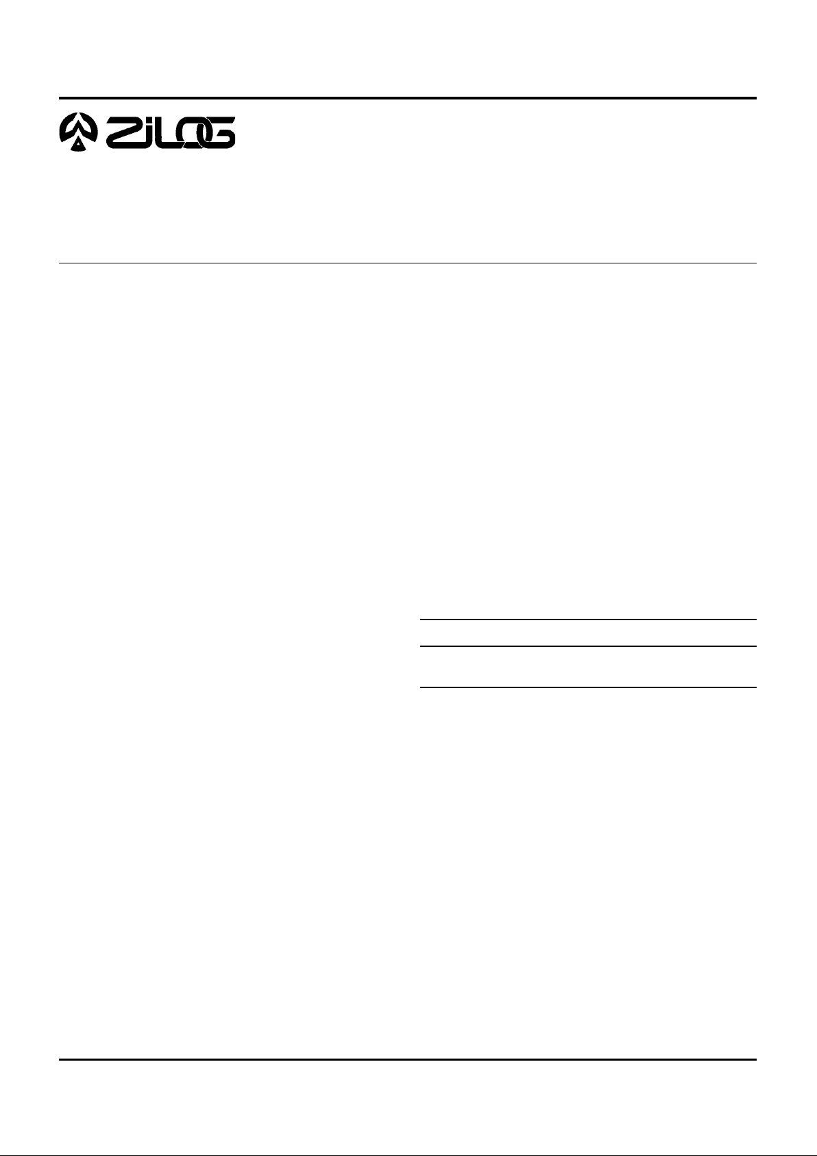
To unburden the program from coping with the real-time problems, such as counting/timing and data communication, the
Z86C90/C89 offers two on-chip counter/timers. Included are a
large number of user selectable modes, and two on-board comparators to process analog signals with a common reference
voltage (see Functional Block Diagram).
Notes:
All Signals with a preceding front slash, "/", are active Low, e.g.: B//W
(WORD is active Low); /B/W (BYTE is active Low, only).
Power connections follow conventional descriptions below:
Connection Circuit Device
Power V
CC
V
DD
Ground GND V
SS
CUSTOMER PROCUREMENT SPECIFICATION
GENERAL DESCRIPTION
DC-4054-01 (10-17-91)
2
GENERAL DESCRIPTION (Continued)
Port 3
Counter/
Timers (2)
Interrupt
Control
Two Analog
Comparators
Port 2
I/O
(Bit Programmable)
ALU
FLAGS
Register
Pointer
Register File
256 x 8-Bit
Machine Timing
&
Instruction Control
Program
Counter
Vcc GND XTAL
44
Port 0
Output Input
Address or I/O
(Nibble Programmable)
8
Port 1
Address/Data or I/O
(Byte Programmable)
/AS /DS
R//W
/RESET
RESET
WDT, POR
Functional Block Diagram
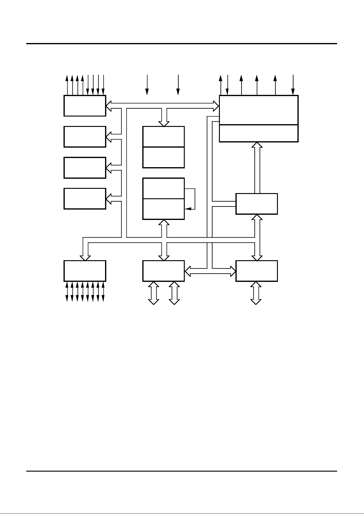
3
1
2
9
3
4
5
6
7
8
40
39
38
37
36
35
34
33
32
/DS
P24
P12
P23
P22
P21
P20
P03
P13
R//W
XTAL2
P27
P04
P05
P06
P14
31
30
29
28
27
14
10
11
12
13
XTAL1
VCC
P16
P17
P25
GND
P02
P11
P10
P01
Z86C90/C89
DIP
15 26
25
24
23
22
21
20
16
17
18
19
P15
P07
P26
P31
P34
/AS
P33
P32
P36
P00
P30
P37
P35
/RESET
PIN DESCRIPTION
40-Pin DIP Pin Assignments
4
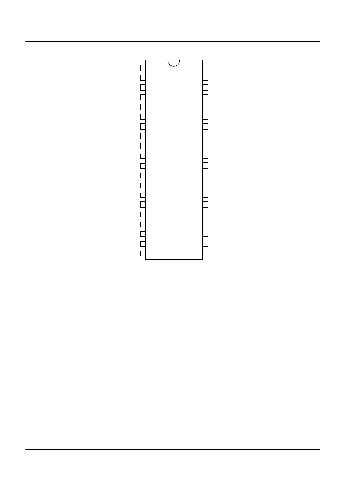
PIN DESCRIPTION (Continued)
P20
P03
P13
P12
GND
GND
P02
P11
P10
P01
P00
P05
P06
P14
P15
P07
VCC
VCC
P16
P17
P30
P36
P37
P35
/RESET
GND
/AS
P34
P33
P32
P31
P21
P22
P23
P24
/DS
N/C
R//W
P25
P26
P27
P04
XTAL1
XTAL2
7
8
9
10
11
12
13
14
15
16
17
38
37
36
35
34
33
32
31
30
29
39
Z86C90/C89
PLCC
6543214443424140
18 19 20 21 22 23 24 25 26 27 28
44-Pin PLCC Pin Assignments
34
35
36
37
38
39
40
41
42
43
44
21
20
19
18
17
16
15
14
13
12
22
33 32 31 30 29 28 27 26 25 24 23
1234567891011
Z86C90/C89
QFP
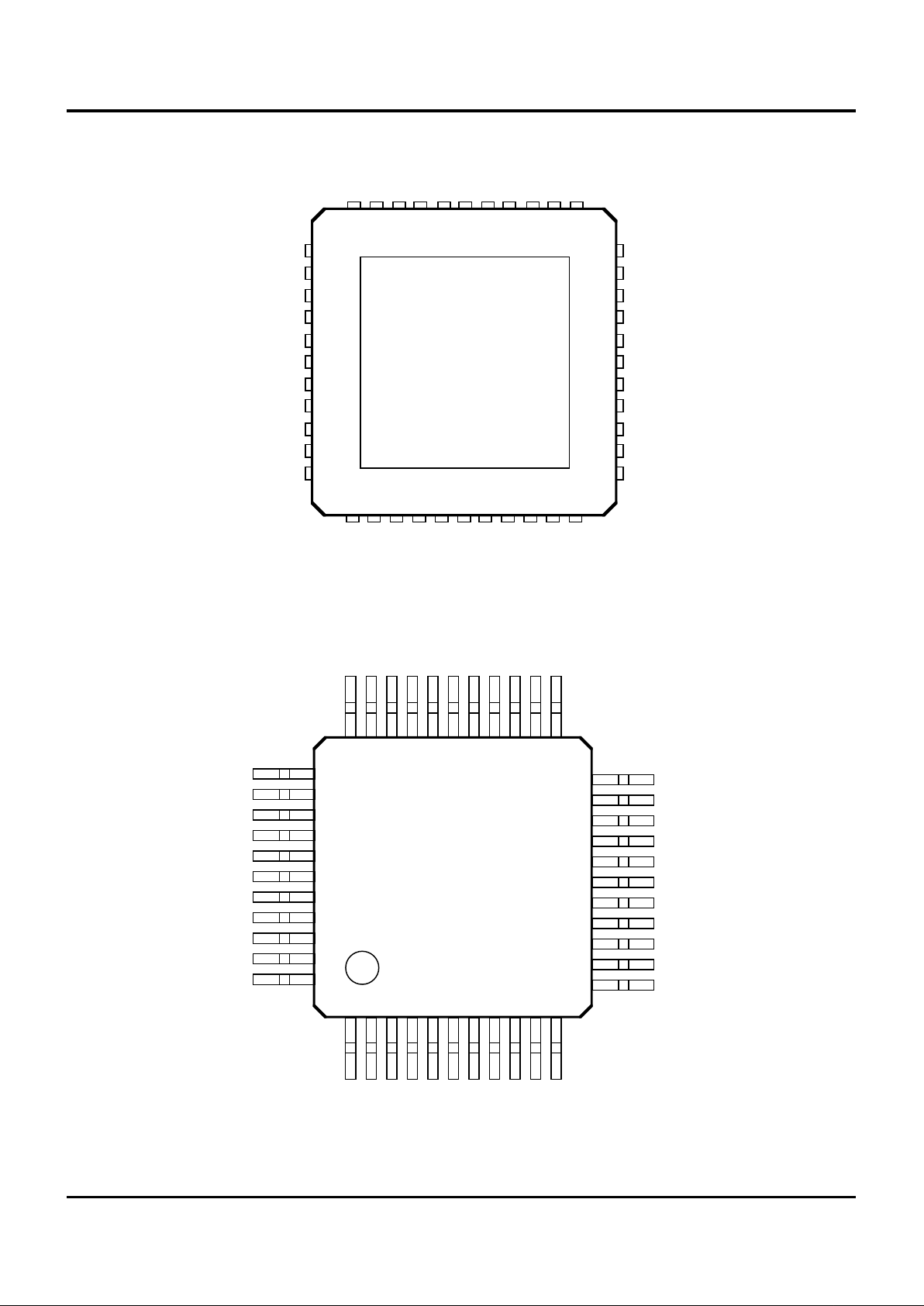
P20
P03
P13
P12
GND
GND
P02
P11
P10
P01
P00
P21
P22
P23
P24
/DS
N/C
R//W
P25
P26
P27
P04
P30
P36
P37
P35
/RESET
GND
/AS
P34
P33
P32
P31
P05
P06
P14
P15
P07
VCC
VCC
P16
P17
XTAL1
XTAL2
44-Pin QFP Pin Assignments
5
STANDARD TEST CONDITIONS
The characteristics listed below apply for standard test conditions
as noted. All voltages are referenced to GND. Positive current
flows into the referenced pin (Test Load Diagram).
Symbol Description Min Max Units
V
CC
Supply Voltage (*) -0.3 +7.0 V
T
STG
Storage Temp -65° +150° C
T
A
Oper Ambient Temp † C
Power Dissipation 2.2 W
Notes:
* Voltage on all pins with respect to GND.
† See Ordering Information.
Stress greater than those listed under Absolute Maximum Rat-
ings may cause permanent damage to the device. This is a stress
rating only; operation of the device at any condition above those
indicated in the operational sections of these specifications is not
implied. Exposure to absolute maximum rating conditions for an
extended
period may affect device reliability.
+5V
From Output
Under Test
150 pF
9.1 KΩ
2.1 KΩ
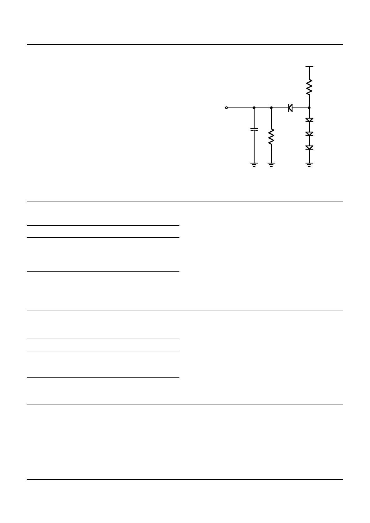
ABSOLUTE MAXIMUM RATINGS
Test Load Diagram
CAPACITANCE
TA = 25°C, VCC = GND = 0V, f = 1.0 MHz, unmeasured pins to GND
Parameter Max
Input capacitance 12 pF
Output capacitance 12 pF
I/O capacitance 12 pF
PLEASE NOTE
These devices will not operate in extended timing mode. Set Register 248, D5 = 0.

6
DC CHARACTERISTICS
Sym Parameter V
CC
TA = 0°CT
A
= -40° C Typ @ Units Conditions
Notes
Note [3] to 70°C to 105° C25°C
Min Max Min Max
Max Input Voltage 3.3V 7 7 V IIN 250µA
5.0V 7 7 V IIN 250µA
V
CH
Clock Input 3.3V 0.7 VCCVCC+0.3 0.7 VCCVCC+0.3 1.3 V Driven by External
High Voltage Clock Generator
5.0V 0.7 VCCVCC+0.3 0.7 VCCVCC+0.3 2.5 V Driven by External
Clock Generator
V
CL
Clock Input 3.3V GND -0.30.2 V
CC
GND-0.3 0.2 V
CC
0.7 V Driven by External
Low Voltage Clock Generator
5.0V GND-0.3 0.2 V
CC
GND-0.3 0.2 V
CC
1.5 V Driven by External
Clock Generator
V
IH
Input High Voltage 3.3V 0.7 VCCVCC+0.3 0.7 VCCVCC+0.3 1.3 V
5.0V 0.7 VCCVCC+0.3 0.7 VCCVCC+0.3 2.5 V
V
IL
Input Low Voltage 3.3V GND-0.3 0.2 V
CC
GND-0.3 0.2 V
CC
0.7 V
5.0V GND-0.3 0.2 V
CC
GND-0.3 0.2 V
CC
1.5 V
V
OH
Output High Voltge 3.3V VCC-0.4 VCC-0.4 3.1 V IOH = -2.0 mA
5.0V VCC-0.4 VCC-0.4 4.8 V IOH = -2.0 mA
V
OL1
Output Low Voltage 3.3V 0.6 0.6 0.2 V IOH = +4.0 mA
5.0V 0.4 0.4 0.1 V IOL = +4.0 mA
V
OL2
Output Low Voltage 3.3V 1.2 1.2 0.3 V IOL = +6 mA,
3 Pin Max
5.0V 1.2 1.2 0.3 V IOL = +12 mA,
3 Pin Max
V
RH
Reset Input 3.3V .8 V
CC
V
CC
.8 V
CC
V
CC
1.5 V
High Voltage 5.0V .8 V
CC
V
CC
.8 V
CC
V
CC
2.1 V
V
Rl
Reset Input 3.3V GND-0.3 0.2 V
CC
GND-0.3 0.2 V
CC
1.1
Low Voltage 5.0V GND-0.3 0.2 V
CC
GND-0.3 0.2 V
CC
1.7
V
OFFSET
Comparator Input 3.3V 25 25 10 mV
Offset Voltage 5.0V 25 25 10 mV
I
IL
Input Leakage 3.3V -1 1 -1 2 < 1 µAVIN = OV, V
CC
5.0V -1 1 -1 2 < 1 µAVIN = OV, V
CC
I
OL
Output Leakage 3.3V -1 1 -1 2 < 1 µAVIN = OV, V
CC
5.0V -1 1 -1 2 < 1 µAVIN = OV, V
CC
I
IR
Reset Input Current 3.3V -45 -60 -20 µA
5.0V -55 -70 -30 µA
I
CC
Supply Current 3.3V 10 10 4 mA @ 8 MHz
[4,5]
5.0V 15 15 10 mA @ 8 MHz
[4,5]
3.3V 15 15 5 mA @ 12 MHz

7
[4,5]
5.0V 20 20 15 mA @ 12 MHz
[4,5]
Sym Parameter V
CC
TA = 0°CT
A
= -40° C Typ @ Units Conditions
Notes
Note [3] to 70°C to 105° C25°C
Min Max Min Max
I
CC1
Standby Current 3.3V 3 3 1 mA HALT Mode
[4,5]
VIN = OV, V
CC
@ 8 MHz
5.0V 5 5 2.4 mA HALT Mode
[4,5]
VIN = OV, V
CC
@ 8 MHz
3.3V 4 4 1.5 mA HALT Mode
[4,5]
VIN = OV, V
CC
@ 12 MHz
5.0V 6 6 3.2 mA HALT Mode
[4,5]
VIN = OV, V
CC
@ 12 MHz
3.3V 2 2 0.8 mA Clock Divide by
[4,5]
16 @ 8 MHz
5.0V 4 4 1.8 mA Clock Divide by
[4,5]
16 @ 8 MHz
3.3V 3 3 1.2 mA Clock Divide by
[4,5]
16 @ 12 MHz
5.0V 5 5 2.5 mA Clock Divide by
[4,5]
16 @ 12 MHz
I
CC2
Standby Current 3.3V 8 15 1 µA STOP Mode [6]
VIN = OV, V
CC
WDT is not Running
5.0V 10 20 2 µA STOP Mode [6]
VIN = OV, V
CC
WDT is not Running
3.3V 500 600 310 µA STOP Mode [6]
VIN =
OV, V
CC
WDT is
Running
5.0V 800
1000 600 µA STOP
Mode
VIN =
OV, V
CC
WDT is

8
R//W
9
1
219
3
1
613
4
5
8 1
8
11
6
1
71015
7
1
4
21
Port 0, /DM
Port 1
/AS
/DS
(Read)
Port1
/DS
(Write)
A7 - A0 D7 - D0 IN
D7 - D0 OUTA7 - A0
AC CHARACTERISTICS
External I/O or Memory Read and Write Timing Diagram
External I/O or Memory Read/Write Timing

9
AC CHARACTERISTICS
External I/O or Memory Read and Write Timing Table
No Symbol Parameter V
CC
TA = 0°C to +70°CT
A
= -40°C to +105°C Units Notes
Note[3] 8 MHz 12 MHz 8 MHz 12 MHz
Min Max Min Max Min Max Min Max
1 TdA(AS) Address Valid to 3.3 55 35 55 35 ns [2]
/AS Rising Delay 5.0 55 35 55 35 ns
2 TdAS(A) /AS Rising to Address 3.3 70 45 70 45 ns [2]
Float Delay 5.0 70 45 70 45 ns
3 TdAS(DR) /AS Rising to Read 3.3 400 250 400 250 ns [1,2]
Data Required Valid 5.0 400 250 400 250 ns
4 TwAS /AS Low Width 3.3 80 55 80 55 ns [2]
5.0 80 55 80 55 ns
5 Td Address Float to 3.3 0 0 0 0 ns
/DS Falling 5.0 0 0 0 0 ns
6 TwDSR /DS (Read) Low Width 3.3 300 200 300 200 ns [1,2]
5.0 300 200 300 200 ns
7 TwDSW /DS (Write) Low Width 3.3 165 110 165 110 ns [1,2]
5.0 165 110 165 110 ns
8 TdDSR(DR) /DS Falling to Read 3.3 260 150 260 150 ns [1,2]
Data Required Valid 5.0 260 160 260 160 ns
9 ThDR(DS) Read Data to 3.3 0 0 0 0 ns [2]
/DS Rising Hold Time 5.0 0 0 0 0 ns
10 TdDS(A) /DS Rising to Address 3.3 85 45 85 45 ns [2]
Active Delay 5.0 95 55 95 55 ns
11 TdDS(AS) /DS Rising to /AS 3.3 60 30 60 30 ns [2]
Falling Delay 5.0 70 45 70 45 ns
12 TdR/W(AS) R//W Valid to /AS 3.3 70 45 70 45 ns [2]
Rising Delay 5.0 70 45 70 45 ns
13 TdDS(R/W) /DS Rising to 3.3 70 45 70 45 ns [2]
R//W Not Valid 5.0 70 45 70 45 ns
14 TdDW(DSW) Write Data Valid to /DS 3.3 80 55 80 55 ns [2]
Falling (Write) Delay 5.0 80 55 80 55 ns
15 TdDS(DW) /DS Rising to Write 3.3 70 45 70 45 ns [2]
Data Not Valid Delay 5.0 80 55 80 55 ns
16 TdA(DR) Address Valid to Read 3.3 475 310 475 310 ns [1,2]
Data Required Valid 5.0 475 310 475 310 ns
17 TdAS(DS) /AS Rising to 3.3 100 65 100 65 ns [2]
/DS Falling Delay 5.0 100 65 100 65 ns
18 TdDI(DS) Data Input Setup to 0.0 115 115 115 115 ns [1,2]
/DS Rising 5.0 75 75 75 75 ns
19 TdDM(AS) /DM Valid to /AS 3.3 55 35 55 35 ns [2]
Falling Delay 5.0 55 35 55 35 ns
Notes:
[1] When using extended memory timing add 2 TpC.
[2] Timing numbers given are for minimum TpC.
[3] 5.0V ±0.5V, 3.3V ±0.3V.
Standard Test Load
All timing references use 0.9 VCC for a logic 1 and 0.1 VCC for a logic 0.

10
Clock
1
3
4
8
2 2 3
T
IRQ
IN
N
6
5
7 7
11
Clock
Setup
1
0
9
Stop
Mode
Recovery
Source
AC CHARACTERISTICS
Additional Timing Diagram
Additional Timing

11
AC CHARACTERISTICS
Additional Timing Table
No Symbol Parameter V
CC
TA = 0°C to 70°CT
A
= -40°C to 105°C Units
Notes
Note[6] 8 MHz 12 MHz 8 MHz 12 MHz
Min Max Min Max Min Max Min Max
1 TpC Input Clock Period 3.3V 125 100000 83 100000 125 100000 83 100000 ns [1]
5.0V 125 100000 83 100000 125 100000 83 100000 ns [1]
2 TrC,TfC Clock Input Rise 3.3V 25 15 25 15 ns [1]
and Fall Times 5.0V 25 15 25 15 ns [1]
3 TwC Input Clock Width 3.3V 37 26 37 26 ns [1]
5.0V 37 26 37 26 ns [1]
4 TwTinL Timer Input 3.3V 100 100 100 100 ns [1]
Low Width 5.0V 70 70 70 70 ns [1]
5 TwTinH Timer Input 3.3V 3TpC 3TpC 3TpC 3TpC [1]
High Width 5.0V 3TpC 3TpC 3TpC 3TpC [1]
6 TpTin Timer Input Period 3.3V 8TpC 8TpC 8TpC 8TpC [1]
5.0V 8TpC 8TpC 8TpC 8TpC [1]
7 TrTin,TfTinTimer Input Rise 3.3V 100 100 100 100 ns [1]
and Fall Timers 5.0V 100 100 100 100 ns [1]
8A TwIL Interrupt Request 3.3V 100 100 100 100 ns [1,2]
Low Time 5.0V 70 70 70 70 ns [1,2]
8B TwIL Int. Request 3.3V 3TpC 3TpC 3TpC 3TpC
[1,3]
Low Time 5.0V 3TpC 3TpC 3TpC 3TpC
[1,3]
9 TwIH Interrupt Request 3.3V 3TpC 3TpC 3TpC 3TpC
[1,2]
Input High Time 5.0V 3TpC 3TpC 3TpC 3TpC
[1,2]
10 Twsm STOP Mode 3.3V 12 12 12 12 ns
Recovery Width Spec 5.0V 12 12 12 12 ns
3.3V 5TpC [7]
5.0V 5TpC [8]

12
AC CHARACTERISTICS
Additional Timing Table (Continued)
No Symbol Parameter V
CC
TA = 0°C to 70°CT
A
= -40°C to 105°C Units Notes
Note[6] 8 MHz 12 MHz 8 MHz 12 MHz
Min Max Min Max Min Max Min Max
11 Tost Oscillator 3.3V 5TpC 5TpC 5TpC 5TpC [4]
Startup Time 5.0V 5TpC 5TpC 5TpC 5TpC [4]
12 Twdt Watchdog Timer 3.3V 10 10 10 10 ms D0 = 0
[5]
Delay Time 5.0V 5555msD1 = 0
[5]
3.3V 30 30 30 30 ms D0 = 1
[5]
5.0V 15 15 15 15 ms D1 = 0
[5]
3.3V 50 50 50 50 ms D0 = 0
[5]
5.0V 25 25 25 25 ms D1 = 1
[5]
3.3V 200 200 200 200 ms D0 = 1
[5]
5.0V 100 100 100 100 ms D1 = 1
[5]
Notes:
[1] Timing Reference uses 0.9 VCC for a logic 1 and 0.1 VCC for a logic 0.
[2] Interrupt request via Port 3 (P31-P33).
[3] Interrupt request via Port 3 (P30).
[4] SMR-D5 = 0
[5] Reg. WDTMR
[6] 5.0V ±0.5V, 3.3V ±0.3V
[7] Reg. SMR - D5=0
[8] Reg. SMR - D5=1

13
Data In
1 2
3
4 5 6
/DAV
(Input)
RDY
(Output)
Next Data In Valid
Delayed RDY
Delayed DAV
Data In Valid
Data Out
/DAV
(Output)
RDY
(Input)
Next Data Out Valid
Delayed RDY
Delayed DAV
Data Out Valid
7
8 9
1
0
11
AC CHARACTERISTICS
Handshake Timing Diagrams
Output Handshake Timing
Input Handshake Timing

14
AC CHARACTERISTICS
Handshake Timing Table
No Symbol Parameter V
CC
TA = 0°C To 70° CT
A
= -40° C To 105° C
Note[1] 8 MHz 12 MHz 8 MHz 12 MHz Data
Min Max Min Max Min Max Min Max Direc-
tion
1 TsDI(DAV) Data In Setup Time 3.3V 0000 IN
5.0V 0000 IN
2 ThDI(DAV) Data In Hold Time 3.3V 160 160 160 160 IN
5.0V 115 115 115 115 IN
3 TwDAV Data Available Width 3.3V 155 155 155 155 IN
5.0V 110 110 110 110 IN
4 TdDAVI(RDY) DAV Falling to RDY 3.3V 160 160 160 160 IN
Falling Delay 5.0V 115 115 115 115 IN
5 TdDAVId(RDY) DAV Rising to RDY 3.3V 120 120 120 120 IN
Falling Delay 5.0V 80 80 80 80 IN
6 TdDO(DAV) RDY Rising to DAV 3.3V 0000 IN
Falling Delay 5.0V 0000 IN
7 TcLDAV0(RDY)Data Out to DAV 3.3V 63 42 63 42 OUT
Falling Delay 5.0V 63 42 63 42 OUT
8 TcLDAV0(RDY)DAV Falling to RDY 3.3V 0000 OUT
Falling Delay 5.0V 0000 OUT
9 TdRDY0(DAV) RDY Falling to DAV 3.3V 160 160 160 160 OUT
Rising Delay 5.0V 115 115 115 115 OUT
10 TwRDY RDY Width 3.3V 110 110 110 110 OUT
5.0V 80 80 80 80 OUT
11 TdRDY0d(DAV)RDY Rising to DAV 3.3V 110 110 110 110 OUT
Falling Delay 5.0V 80 80 80 80 OUT
Note:
[1] 5.0 V ±0.5V, 3.3V ±0.3V
responsible for any errors that may appear in this document. Zilog, Inc.
makes no commitment to update or keep current the information
contained in this document.
Zilog, Inc. 210 East Hacienda Ave.
Campbell, CA 95008-6600
Telephone (408) 370-8000
Telex 171-980 A/B ZILOG CPTO
FAX 408 370-8056/8027
© 1991 by Zilog, Inc. All rights reserved. No part of this document may
be copied or reproduced in any form or by any means without the prior
written consent of Zilog, Inc. The information in this document is subject
to change without notice. Devices sold by Zilog, Inc. are covered by
warranty and patent indemnification provisions appearing in Zilog, Inc.
Terms and Conditions of Sale only. Zilog, Inc. makes no warranty,
express, statutory, implied or by description, regarding the information
set forth herein or regarding the freedom of the described devices from
intellectual property infringement. Zilog, Inc. makes no warranty of
merchantability or fitness for any purpose. Zilog, Inc. shall not be
 Loading...