

Datasheet Z86C0412PSC, Z86C0412SAC, Z86C0412SEC, Z86C0412SSC, Z86C0412PAC Datasheet (ZILOG)
...
DS97DZ80502
P R E L I M I N A R Y
1
1
P
RELIMINARY
P
RODUCT
S
PECIFICATION
Z86C04/C08
1
CMOS 8-B
IT
L
OW
-C
OST
1K/2K-ROM M
ICROCONTROLLERS
FEATURES
■
18-Pin DIP and SOIC Packages
■
3.0V to 5.5V Operating Range
■
Available Temperature Ranges
A = –40 ° C to +125 ° C
E = –40 ° C to +105 ° C
S = 0 ° C to +70 ° C
■
14 Input / Output Lines
■
Six Vectored, Prioritized Interrupts from Six Different
Sources
■
Two On-Board Comparators
■
ROM Mask Options:
– Low Noise
– ROM Protect
– Auto Latch
– System Clock Driving WDT (Z86C04 only)
– Permanent Watch-Dog Timer (WDT)
– RC Oscillator
– 32 kHz Operation
■
Two Programmable 8-Bit Counter/Timers,
Each with 6-Bit Programmable Prescaler
■
Power-On Reset (POR) Timer
■
On-Chip Oscillator that Accepts RC, Crystal,
Ceramic Resonance, LC, or External Clock Drive
■
Clock-Free WDT Reset
■
Low-Power Consumption (50mw)
■
Fast Instruction Pointer
(1.0 µ s @ 12 MHz)
■
Fourteen Digital Inputs at CMOS Levels;
Schmitt-Triggered
■
Software Enabled Watch-Dog Timer
■
Programmable Interrupt Polarity
■
Two Standby Modes: STOP and HALT
■
Low-Voltage Protection
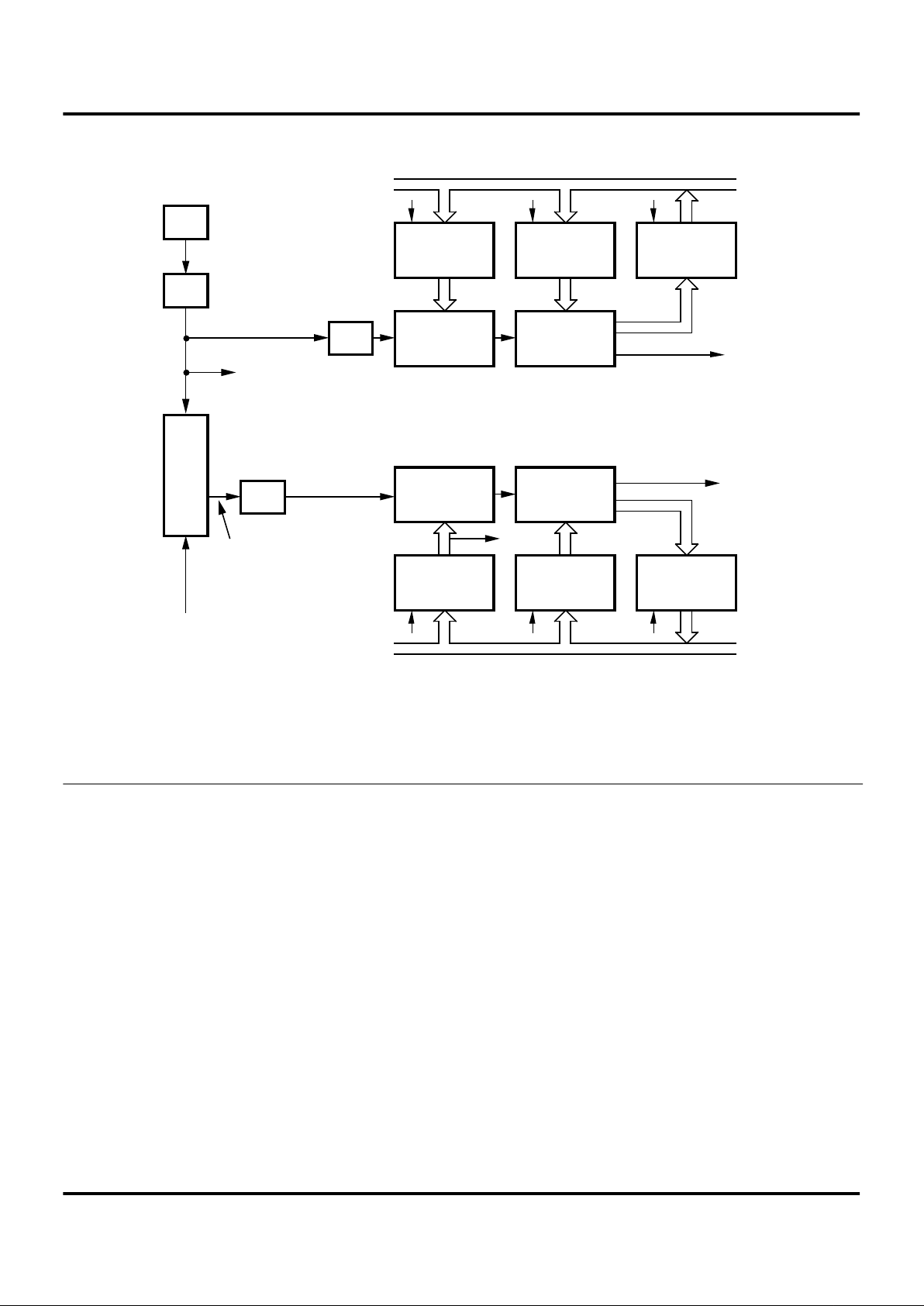
GENERAL DESCRIPTION
Zilog’s Z86C04/C08 are members of the Z8
®
MCU singlechip microcontroller family which offer easy software/hardware system expansion .
For applications demanding powerful I/O capabilities, the
Z86C04/C08’s dedicated input and output lines are
grouped into three ports, and are configurable under software control to provide timing, status signals, or parallel
I/O.
Two on-chip counter/timers, with a large number of user
selectable modes, off-load the system of administering
real-time tasks such as counting/timing and I/O data communications. Additionally, two on-board comparators process analog signals with a common reference voltage (Figure 1).
Part
Number
ROM
(KB)
RAM*
(Bytes)
Speed
(MHz)
Auto
Latch
Permanent
WDT
Z86C04
Z86C0812
125
125
1212Optional
Optional
Optional
Optional
Note: * General-Purpose
Z86C04/C08
CMOS 8-Bit Low-Cost 1K/2K-ROM Microcontrollers Zilog
2
P R E L I M I N A R Y
DS97DZ80502
GENERAL DESCRIPTION (Continued)
Note: All Signals with a preceding front slash, "/", are
active Low, e.g.: B//W (WORD is active Low); /B/W (BYTE
is active Low, only).
Power connections follow conventional descriptions below:
Connection Circuit Device
Power
Ground
V
CC
GND
V
DD
V
SS
Figure 1. Z86C04/C08
Functional Block Diagram
Port 3
Counter/
Timers (2)
Interrupt
Control
T wo Analog
Comparators
Port 2
I/O
(Bit Programmable)
ALU
FLAG
Register
Pointer
Register File
Machine
Timing & Inst.
Control
Prg. Memory
Program
Counter
Vcc GND XTALVcc
Input
Port 0
I/O
Z86C04/C08
Zilog CMOS 8-Bit Low-Cost 1K/2K-ROM Microcontrollers
DS97DZ80502
P R E L I M I N A R Y
3
1
PIN DESCRIPTIONS
Figure 2. 18-Pin DIP Configuration
1
2
9
3
4
5
6
7
8
18
17
16
15
14
13
12
11
10
P23
P22
P33
P21
P20
GND
P02
P01
P00
P24
P25
P32
P26
P27
VCC
XTAL2
XTAL1
P31
DIP
Table 1: 18-Pin DIP and SOIC Pin Identification
Pin # Symbol Function Direction
1-4
5
6
7
8
P24-P27
V
CC
XTAL2
XTAL1
P31
Port 2, Pins 4, 5, 6, 7
Power Supply
Crystal Oscillator Clock
Crystal Oscillator Clock
Port 3, Pin 1, AN1
In/Output
Output
Input
Input
9
10
11-13
14
15-18
P32
P33
P00-P02
GND
P20-P23
Port 3, Pin 2, AN2
Port 3, Pin 3, REF
Port 0, Pins 0, 1, 2
Ground
Port 2, Pins 0, 1, 2, 3
Input
Input
In/Output
In/Output
Figure 3. 18-Pin SOIC Pin Configuration
1
18
P24
P27
Vcc
XTAL2
XTAL1
P31
P32
P23
P22
P21
P20
GND
P02
P01
P00
P33
SOIC
P25
P26
2
3
4
5
6
7
8
9
17
16
15
14
13
12
11
10
Z86C04/C08
CMOS 8-Bit Low-Cost 1K/2K-ROM Microcontrollers Zilog
4
P R E L I M I N A R Y
DS97DZ80502
ABSOLUTE MAXIMUM RATINGS
Stresses greater than those listed under Absolute Maximum Ratings may cause permanent damage to the device. This is a stress rating only; functional operation of the
device at any condition above those indicated in the operational sections of these specifications is not implied. Exposure to absolute maximum rating conditions for an ex-
tended period may affect device reliability. Total power
dissipation should not exceed 462 mW for the package.
Power dissipation is calculated as follows:
Total Power dissipation = V
DD
x [I
DD
– (sum of I
OH
)] + sum of
[(V
DD
– V
OH
) x I
OH
] + sum of (V
0L
x I
0L
).
STANDARD TEST CONDITIONS
The characteristics listed below apply for standard test
conditions as noted. All voltages are referenced to
Ground. Positive current flows into the referenced pin
(Figure 4).
Parameter Min Max Units
Ambient Temperature under Bias –40 +105 C
Storage Temperature –65 +150 C
Voltage on any Pin with Respect to V
SS
[Note 1] –0.7 +12 V
Voltage on V
DD
Pin with Respect to V
SS
–0.3 +7 V
Voltage on Pin 7 with Respect to V
SS
[Note 2] –0.7 V
DD
+1 V
Total Power Dissipation 462 mW
Maximum Current out of V
SS
84 mA
Maximum Current into V
DD
84 mA
Maximum Current into an Input Pin [Note 3] –600 +600
µ
A
Maximum Current into an Open-Drain Pin [Note 4] –600 +600
µ
A
Maximum Output Current Sinked by Any I/O Pin 12 mA
Maximum Output Current Sourced by Any I/O Pin 12 mA
Total Maximum Output Current Sinked by Port 2 70 mA
Total Maximum Output Current Sourced by Port 2 70 mA
Notes:
1. This applies to all pins except where otherwise noted. Maximum current into pin must be ± 600 µ A.
2. There is no input protection diode from pin to V
DD
.
3. This excludes Pin 6 and Pin 7.
4. Device pin is not at an output Low state.
Figure 4. Test Load Diagram
From Output
Under Test
150 pF
Z86C04/C08
Zilog CMOS 8-Bit Low-Cost 1K/2K-ROM Microcontrollers
DS97DZ80502
P R E L I M I N A R Y
5
1
CAPACITANCE
T
A
= 25 ° C, V
CC
= GND = 0V, f = 1.0 MHz, unmeasured pins returned to GND.
DC ELECTRICAL CHARACTERISTICS
Parameter Min Max
Input capacitance 0 15 pF
Output capacitance 0 20 pF
I/O capacitance 0 25 pF
T
A
= –40 ° C
to +125 ° C
Typical
Sym Parameter
V
CC
[4]
Min Max @ 25 ° C Units Conditions Notes
V
CH
Clock Input High
Voltage
3.0V 0.8 V
CC
V
CC
+0.3 1.7 V Driven by External
Clock Generator
5.5V 0.8 VCCVCC+0.3 2.8 V Driven by External
Clock Generator
V
CL
Clock Input Low
Voltage
3.0V VSS–0.3 0.2 V
CC
0.8 V Driven by External
Clock Generator
5.5V VSS–0.3 0.2 V
CC
1.7 V Driven by External
Clock Generator
V
IH
Input High Voltage 3.0V 0.7 V
CCVCC
+0.3 1.8 V 1
5.5V 0.7 V
CCVCC
+0.3 2.8 V 1
V
IL
Input Low Voltage 3.0V VSS–0.3 0.2 V
CC
0.8 V 1
5.5V V
SS
–0.3 0.2 V
CC
1.5 V 1
V
OH
Output High
Voltage
3.0V VCC–0.4 3.0 V IOH = –2.0 mA 5
5.5V V
CC
–0.4 4.8 V IOH = –2.0 mA 5
3.0V V
CC
–0.4 3.0 V Low Noise @ I
OH
= –0.5 mA
5.5V V
CC
–0.4 4.8 V Low Noise @ IOH = –0.5 mA
V
OL1
Output Low Voltage 3.0V 0.8 0.2 V IOL = +4.0 mA 5
5.5V 0.6 0.1 V I
OL
= +4.0 mA 5
3.0V 0.6 0.2 V Low Noise @ I
OL
= 1.0 mA
5.5V 0.6 0.1 V Low Noise @ I
OL
= 1.0 mA
V
OL2
Output Low Voltage 3.0V 1.2 0.8 V IOL = +12 mA 5
5.5V 1.0 0.3 V I
OL
= +12 mA 5
V
OFFSET
Comparator Input
Offset V oltage
3.0V 25 10 mV
5.5V 25 10 mV
V
LV
VCC Low Voltage
Auto Reset
1.8 3.0 2.6 V Int. CLK Freq @ 2 MHz Max.
I
IL
Input Leakage
(Input Bias
Current of
Comparator)
3.0V –1.0 1.0 µAVIN = 0V, V
CC
5.5 –1.0 1.0 µAVIN = 0V, V
CC
I
OL
Output Leakage 3.0V –1.0 1.0 µAVIN = 0V, V
CC
5.5V –1.0 1.0 µAVIN = 0V, Vcc

Z86C04/C08
CMOS 8-Bit Low-Cost 1K/2K-ROM Microcontrollers Zilog
6 P R E L I M I N A R Y DS97DZ80502
DC ELECTRICAL CHARACTERISTICS (Continued)
V
VICR
Comparator Input
Common Mode
Voltage Range
0VCC –1.5 V
I
CC
Supply Current 3.0V 3.5 1.5 mA All Output and I/O Pins Floating
@ 2 MHz
5,7
5.5V 7.0 3.8 mA All Output and I/O Pins Floating
@ 2 MHz
5,7
3.0V 8.0 3.0 mA All Output and I/O Pins Floating
@ 8 MHz
5,7
5.5V 11.0 4.4 mA All Output and I/O Pins Floating
@ 8 MHz
5,7
3.0V 10 3.6 mA All Output and I/O Pins Floating
@ 12 MHz
5,7
5.5V 15 9.0 mA All Output and I/O Pins Floating
@ 12 MHz
5,7
I
CC1
Standby Current 3.0V 2.5 0.7 mA HALT mode V
IN
= 0V,
VCC @ 2 MHz
5,7
5.5V 4.0 2.5 mA HALT mode V
IN
= 0V,
V
CC
@ 2 MHz
5,7
3.0V 4.0 1.0 mA HALT mode V
IN
= 0V,
VCC @ 8 MHz
5,7
5.5V 5.0 3.0 mA HALT mode V
IN
= 0V,
VCC @ 8 MHz
5,7
3.0V 4.5 1.5 mA HALT mode V
IN
= 0V,
VCC @ 12 MHz
5,7
5.5V 7.0 4.0 mA HALT mode V
IN
= 0V,
VCC @ 12 MHz
5,7
I
CC
Supply Current
(Low Noise Mode)
3.0V 3.5 1.5 mA All Output and I/O Pins Floating
@ 1 MHz
7
5.5V 7.0 3.8 mA All Output and I/O Pins Floating
@ 1 MHz
7
3.0V 5.8 2.5 mA All Output and I/O Pins Floating
@ 2 MHz
7
5.5V 9.0 4.0 mA All Output and I/O Pins Floating
@ 2 MHz
7
3.0V 8.0 3.0 mA All Output and I/O Pins Floating
@ 4 MHz
7
5.5V 11.0 4.4 mA All Output and I/O Pins Floating
@ 4 MHz
7
Z86C04/C08
CMOS 8-Bit Low-Cost 1K/2K-ROM Microcontrollers Zilog
7 P R E L I M I N A R Y DS97DZ80502
DC ELECTRICAL CHARACTERISTICS (Continued)
T
A
= –40°C
to +125°C
Typical
Sym Parameter
V
CC
[4]
Min Max @ 25°C Units Conditions Notes
I
CC1
Standby Current
(Low Noise Mode)
3.0V 2.5 0.7 mA HALT mode V
IN
= 0V, VCC @ 1MHz 7
5.5V 4.0 2.5 mA HALT mode V
IN
= 0V, VCC @ 1MHz
3.0V 3.0 0.9 mA HALT mode V
IN
= 0V, VCC @ 2 MHz 7
5.5V 4.5 2.8 mA HALT mode V
IN
= 0V, VCC @ 2 MHz 7
3.0V 4.0 1.0 mA HALT mode V
IN
= 0V, VCC @ 4 MHz 7
5.5V 5.0 3.0 mA HALT mode V
IN
= 0V, VCC @ 4 MHz 7
I
CC2
Standby Current 3.0V 20 1.0 µA STOP mode VIN = 0V, VCC ;WDT is not
Running
7
5.5V 20 1.0 µA STOP mode V
IN
= 0V, VCC ;WDTis not
Running
7
I
ALL
Auto Latch Low Current 3.0V 8.0 3.0 µA 0V < VIN < V
CC
5.5V 30 16 µA 0V < VIN < V
CC
I
ALH
Auto Latch High Current 3.0V –5.0 –1.5 µA 0V < VIN < V
CC
5.5V –20 –8.0 µA 0V < VIN < V
CC
Notes:
1. Port 0, 2, and 3 only.
2. V
SS
= 0V = GND.
3. The device operates down to V
LV
. The minimum operational VCC is determined on the value of the voltage VLV at the ambient
temperature. The V
LV
increases as the temperature decreases.
4. V
CC
= 3.0V to 5.5V, typical values measured at VCC = 3.3V and VCC = 5.0V.
5. Standard Mode (not Low EMI mode).
6. Z86C08 only.
7. Inputs at power rail and outputs are unloaded.
Z86C04/C08
CMOS 8-Bit Low-Cost 1K/2K-ROM Microcontrollers Zilog
8 P R E L I M I N A R Y DS97DZ80502
DC ELECTRICAL CHARACTERISTICS (Continued)
TA= 0°C to
+70°C
TA= –40°C to
+105°C
Typical
Symbol Parameter
V
CC
Min Max Min Max @ 25°C Units Conditions Notes
V
CH
Clock Input High
Voltage
3.0V 0.8 VCCVCC+0.3 0.8 VCCVCC+0.3 1.7 V Driven by External
Clock Generator
5.5V 0.8 VCCVCC+0.3 0.8 VCCVCC+0.3 2.8 V Driven by External
Clock Generator
V
CL
Clock Input Low
Voltage
3.0V VSS–0.3 0.2 VCCVSS–0.3 0.2 V
CC
0.8 V Driven by External
Clock Generator
5.5V VSS–0.3 0.2 VCCVSS–0.3 0.2 V
CC
1.7 V Driven by External
Clock Generator
V
IH
Input High Voltage 3.0V 0.7 VCCVCC+0.3 0.7 VCCVCC+0.3 1.8 V 1
5.5V 0.7 V
CCVCC
+0.3 0.7 VCCVCC+0.3 2.8 V 1
V
IL
Input Low Voltage 3.0V VSS–0.3 0.2 VCCVSS–0.3 0.2 V
CC
0.8 V 1
5.5V V
SS
–0.3 0.2 VCCVSS–0.3 0.2 V
CC
1.5 V 1
V
OH
Output High Voltage 3.0V VCC–0.4 VCC–0.4 3.0 V IOH = –2.0 mA 5
5.5V V
CC
–0.4 VCC–0.4 4.8 V IOH = –2.0 mA 5
3.0V V
CC
–0.4 VCC–0.4 3.0 V Low Noise @
IOH = –0.5 mA
5.5V V
CC
–0.4 VCC–0.4 4.8 V Low Noise @
IOH = –0.5 mA
V
OL1
Output Low Voltage 3.0V 0.8 0.8 0.2 V IOL= +4.0 mA 5
5.5V 0.4 0.4 0.1 V I
OL
= +4.0 mA 5
3.0V 0.4 0.4 0.2 V Low Noise @
I
OL
= 1.0 mA
5.5V 0.4 0.4 0.1 V Low Noise @
I
OL
= 1.0 mA
V
OL2
Output Low Voltage 3.0V 1.0 1.0 0.8 V IOL = +12 mA 5
5.5V 0.8 0.8 0.3 V I
OL
= +12 mA 5
V
OFFSET
Comparator Input
Offset V oltage
3.0V 25 25 10 mV
5.5V 25 25 10 mV
V
LV
VCC Low Voltage
Auto Reset
2.2 2.8 2.6 V Int. CLK Freq @
6 MHz Max.
2.0 3.0 2.6 V Int. CLK Freq @
4 MHz Max.
I
IL
Input Leakage
(Input Bias Current
of Comparator)
3.0V –1.0 1.0 –1.0 1.0 µAVIN = 0V, V
CC
5.5V –1.0 1.0 –1.0 1.0 µAVIN = 0V, V
CC
I
OL
Output Leakage 3.0V –1.0 1.0 –1.0 1.0 µAVIN = 0V, V
CC
5.5V –1.0 1.0 –1.0 1.0 µAVIN = 0V, V
CC
V
VICR
Comparator Input
Common Mode
Voltage Range
0VCC–1.0 0 VCC–1.5 V

Z86C04/C08
CMOS 8-Bit Low-Cost 1K/2K-ROM Microcontrollers Zilog
9 P R E L I M I N A R Y DS97DZ80502
DC ELECTRICAL CHARACTERISTICS (Continued)
Icc
Supply Current 3.0V 3.5 3.5 1.5 mA All Output and I/O
Pins Floating @
2 MHz
5,7
5.5V 7.0 7.0 3.8 mA All Output and I/O
Pins Floating @
2 MHz
5,7
3.0V 8.0 8.0 3.0 mA All Output and I/O
Pins Floating @
8 MHz
5,7
5.5V 11.0 11.0 4.4 mA All Output and I/O
Pins Floating @
8 MHz
5,7
3.0V 10 10 3.6 mA All Output and I/O
Pins Floating @
12 MHz
5,7
5.5V 15 15 9.0 mA All Output and I/O
Pins Floating @
12 MHz
5,7
I
CC1
Standby Current 3.0V 2.5 2.5 0.7 mA HALT mode V
IN
= 0V ,
VCC @ 2 MHz
5,7
5.5V 4.0 4.0 2.5 mA HAL T mode V
IN
= 0V ,
VCC @ 2 MHz
5,7
3.0V 4.0 4.0 1.0 mA HAL T mode V
IN
= 0V ,
VCC @ 8 MHz
5,7
5.5V 5.0 5.0 3.0 mA HAL T mode V
IN
= 0V ,
V
CC
@ 8 MHz
5,7
3.0V 4.5 4.5 1.5 mA HAL T mode V
IN
= 0V ,
VCC @ 12 MHz
5,7
5.5V 7.0 7.0 4.0 mA HAL T mode V
IN
= 0V ,
VCC @ 12 MHz
5,7
T
A
= 0°C to
+70°C
TA= –40°C to
+105°C
Typical
Symbol Parameter
V
CC
Min Max Min Max @ 25°C Units Conditions Notes

Z86C04/C08
CMOS 8-Bit Low-Cost 1K/2K-ROM Microcontrollers Zilog
10 P R E L I M I N A R Y DS97DZ80502
DC ELECTRICAL CHARACTERISTICS (Continued)
I
CC
Supply Current
(Low Noise)
3.0V 3.5 3.5 1.5 mA All Output and I/O
Pins Floating @
1 MHz
7
5.5V 7.0 7.0 3.8 mA All Output and I/O
Pins Floating @
1 MHz
7
3.0V 5.8 5.8 2.5 mA All Output and I/O
Pins Floating @
2 MHz
7
5.5V 9.0 9.0 4.0 mA All Output and I/O
Pins Floating @
2 MHz
7
3.0V 8.0 8.0 3.0 mA All Output and I/O
Pins Floating @
4 MHz
7
5.5V 11.0 11.0 4.4 mA All Output and I/O
Pins Floating @
4 MHz
7
T
A
= 0°C to
+70°C
TA= –40°C to
+105°C
Typical
Symbol Parameter
V
CC
Min Max Min Max @ 25°C Units Conditions Notes

Z86C04/C08
Zilog CMOS 8-Bit Low-Cost 1K/2K-ROM Microcontrollers
DS97DZ80502 P R E L I M I N A R Y 11
1
I
CC1
Standby Current
(Low Noise Mode)
3.0V 2.5 2.5 0.7 mA HAL T mode V
IN
= 0V ,
VCC @ 2 MHz
5,7
5.5V 4.0 4.0 2.5 mA HAL T mode V
IN
= 0V ,
V
CC
@ 2 MHz
5,7
3.0V 3.0 3.0 0.9 mA HAL T mode V
IN
= 0V ,
VCC @ 8 MHz
5,7
5.5V 4.5 4.5 2.8 mA HAL T mode V
IN
= 0V ,
VCC @ 8 MHz
5,7
3.0V 4.0 4.0 1.0 mA HAL T mode V
IN
= 0V ,
VCC @ 12 MHz
5,7
5.5V 5.0 5.0 3.0 mA HAL T mode V
IN
= 0V ,
VCC @ 12 MHz
5,7
I
CC2
Standby Current 3.0V 10 20 1.0 µA STOP mode VIN =
0V,Vcc WDT is not
Running
7
5.5V 10 20 1.0 µA STOP mode VIN =
0V,Vcc WDT is not
Running
7
I
ALL
Auto Latch Low
Current
3.0V 12 8.0 3.0 µA 0V < VIN < V
CC
5.5V 32 30 16 µA 0V < VIN < V
CC
I
ALH
Auto Latch High
Current
3.0V –8 –5.0 –1.5 µA 0V < VIN < V
CC
5.5V –16 –20 –8.0 µA 0V < VIN < V
CC
Notes:
1. Port 0, 2, and 3 only.
2. V
SS
= 0V = GND.
3. The device operates down to V
LV
. The minimum operational VCC is determined on the value of the voltage VLV at the ambient
temperature. The V
LV
increases as the temperature decreases.
4. V
CC
= 3.0V to 5.5V, typical values measured at VCC = 3.3V and VCC = 5.0V.
5. Standard Mode (not Low EMI mode).
6. Z86C08 only.
7. Inputs at power rail and outputs are unloaded.
TA= 0°C to
+70°C
TA= –40°C to
+105°C
Typical
Symbol Parameter
V
CC
Min Max Min Max @ 25°C Units Conditions Notes

Z86C04/C08
CMOS 8-Bit Low-Cost 1K/2K-ROM Microcontrollers Zilog
12 P R E L I M I N A R Y DS97DZ80502
Figure 5. AC Electrical Timing Diagram
1
3
4
8
223
T
IRQ
IN
N
6
5
7
7
9
Clock

Z86C04/C08
Zilog CMOS 8-Bit Low-Cost 1K/2K-ROM Microcontrollers
DS97DZ80502 P R E L I M I N A R Y 13
1
AC ELECTRICAL CHARACTERISTICS
Timing Table (Standard Mode for SCLK/TCLK = XTAL/2)
TA = -40C to +125C
8 MHz 12 MHz
No Symbol Parameter
V
CC
Min Max Min Max Units Notes
1 TpC Input Clock Period 3.0V 125 DC 83 DC ns 1
5.5V 125 DC 83 DC ns 1
2 TrC,TfC Clock Input Rise
and Fall Times
3.0V 25 15 ns 1
5.5V 25 15 ns 1
3 TwC Input Clock Width 3.0V 62 41 ns 1
5.5V 62 41 ns 1
4 TwTinL Timer Input Low Width 3.0V 100 100 ns 1
5.5V 70 70 ns 1
5 TwTinH Timer Input High Width 3.0V 5TpC 5TpC 1
5.5V 5TpC 5TpC 1
6 TpTin Timer Input Period 3.0V 8TpC 8TpC 1
5.5V 8TpC 8TpC 1
7 TrTin,
TtTin
Timer Input Rise
and Fall Time
3.0V 100 100 ns 1
5.5V 100 100 ns 1
8 TwIL Int. Request Input
Low Time
3.0V 100 100 ns 1,2
5.5V 70 70 ns 1,2
9 TwIH Int. Request Input
High Time
3.0V 5TpC 5TpC 1
5.5V 5TpC 5TpC 1,2
10 Twdt Watch-Dog Timer
Delay Time Before
Timeout
3.0V 25 25 ms
5.5V 10 10 ms
11 Tpor Power-On Reset Time 3.0V 50 180 50 180 ms 3
5.5V 20 100 20 100 ms 3
3.0V 4 60 4 60 ms 4
5.5V 2 30 2 30 ms 4
Notes:
1. Timing Reference uses 0.7 V
CC
for a logic 1 and 0.2 VCC for a logic 0.
2. Interrupt request through Port 3 (P33-P31).
3. Z86C08.
4. Z86C04

Z86C04/C08
CMOS 8-Bit Low-Cost 1K/2K-ROM Microcontrollers Zilog
14 P R E L I M I N A R Y DS97DZ80502
T
A
= 0°C to +70°C
T
A
= -40°C to +105°C
8 MHz 12 MHz 8 MHz 12 MHz
No Symbol Parameter
V
CC
Min Max Min Max Min Max Min Max Units Notes
1 TpC Input Clock Period 3.0V 125 DC 83 DC 125 DC 83 DC ns 1
5.5V 125 DC 83 DC 125 DC 83 DC ns 1
2 TrC,TfC Clock Input Rise
and Fall Times
3.0V 25 15 25 15 ns 1
5.5V 25 15 25 15 ns 1
3 TwC Input Clock Width 3.0V 62 41 62 41 ns 1
5.5V 62 41 62 41 ns 1
4 TwTinL Timer Input Low
Width
3.0V 100 100 100 100 ns 1
5.5V 70 70 70 70 ns 1
5 TwTinH Timer Input High
Width
3.0V 5TpC 5TpC 5TpC 5TpC 1
5.5V 5TpC 5TpC 5TpC 5TpC 1
6 TpTin Timer Input Period 3.0V 8TpC 8TpC 8TpC 8TpC 1
5.5V 8TpC 8TpC 8TpC 8TpC 1
7 TrTin,
TtTin
Timer Input Rise
and Fall Time
3.0V 100 100 100 100 ns 1
5.5V 100 100 100 100 ns 1
8 TwIL Int. Request Input
Low Time
3.0V 100 100 100 100 ns 1,2
5.5V 70 70 70 70 ns 1,2
9 TwIH Int. Request Input
High Time
3.0V 5TpC 5TpC 5TpC 5TpC 1
5.5V 5TpC 5TpC 5TpC 5TpC 1,2
10 T wdt Watch-Dog Timer
Delay Time
Before Timeout
3.0V 25 25 25 25 ms
5.5V 12 12 10 10 ms
11 Tpor Power-On Reset
Time
3.0V 50 160 50 160 50 160 50 160 ms 3
5.5V 20 80 20 80 20 80 20 80 ms 3
3.0V 4 38 4 38 4 38 4 38 ms 4
5.5V 3 18 3 18 2 18 2 18 ms 4
Notes:
1. Timing Reference uses 0.7 V
CC
for a logic 1 and 0.2 VCC for a logic 0.
2. Interrupt request through Port 3 (P33-P31).
3. Z86C08.
4. Z86C04
Z86C04/C08
CMOS 8-Bit Low-Cost 1K/2K-ROM Microcontrollers Zilog
15 P R E L I M I N A R Y DS97DZ80502
AC ELECTRICAL CHARACTERISTICS
Low Noise Mode (SCLK/TCLK = XTAL)
TA= –40°C to +125°C
1 MHz 4 MHz
No Symbol Parameter
V
CC
Min Max Min Max Units Notes
1 TpC Input Clock Period 3.0V 1000 DC 250 DC ns 1
5.5V 1000 DC 250 DC ns 1
2 TrC,TfC Clock Input Rise
and Fall Times
3.0V 25 25 ns 1
5.5V 25 25 ns 1
3 TwC Input Clock Width 3.0V 500 125 ns 1
5.5V 500 125 ns 1
4 TwTinL Timer Input Low Width 3.0V 100 100 ns 1
5.5V 70 70 ns 1
5 TwTinH Timer Input High Width 3.0V 2.5TpC 2.5TpC 1
5.5V 2.5TpC 2.5TpC 1
6 TpTin Timer Input Period 3.0V 4TpC 4TpC 1
5.5V 4TpC 4TpC 1
7 TrTin,
TtTin
Timer Input Rise
and Fall Time
3.0V 100 100 ns 1
5.5V 100 100 ns 1
8 TwIL Int. Request Input
Low Time
3.0V 100 100 ns 1,2
5.5V 70 70 ns 1,2
9 TwIH Int. Request Input
High Time
3.0V 2.5TpC 2.5TpC 1
5.5V 2.5TpC 2.5TpC 1,2
10 Twdt Watch-Dog Timer
Delay Time Before Timeout
3.0V 25 25 ms 3
5.5V 10 10 ms 3
Notes:
1. Timing Reference uses 0.7 V
CC
for a logic 1 and 0.2 VCC for a logic 0.
2. Interrupt request through Port 3 (P33-P31).
3. Internal RC Oscillator driving WDT.
Z86C04/C08
CMOS 8-Bit Low-Cost 1K/2K-ROM Microcontrollers Zilog
16 P R E L I M I N A R Y DS97DZ80502
T
A
= 0°C to 70°CT
A
= –40°C to +105°C
1 MHz 4 MHz 1 MHz 4 MHz
No Symbol Parameter
V
CC
Min Max Min Max Min Max Min Max Units Notes
1 TpC Input Clock Period 3.0V 1000 DC 250 DC 1000 DC 250 DC ns 1
5.5V 1000 DC 250 DC 1000 DC 250 DC ns 1
2 TrC,TfC Clock Input Rise
and Fall Times
3.0V 25 25 25 25 ns 1
5.5V 25 25 25 25 ns 1
3 TwC Input Clock Width 3.0V 500 125 500 125 ns 1
5.5V 500 125 500 125 ns 1
4 TwTinL Timer Input Low Width 3.0V 100 100 100 100 ns 1
5.5V 70 70 70 70 ns 1
5 TwTinH Timer Input High Width 3.0V 2.5TpC 2.5TpC 2.5TpC 2.5TpC 1
5.5V 2.5TpC 2.5TpC 2.5TpC 2.5TpC 1
6 TpTin Timer Input Period 3.0V 4TpC 4TpC 4TpC 4TpC 1
5.5V 4TpC 4TpC 4TpC 4TpC 1
7 TrTin,
TtTin
Timer Input Rise
and Fall Timer
3.0V 100 100 100 100 ns 1
5.5V 100 100 100 100 ns 1
8 TwIL Int. Request Input
Low Time
3.0V 100 100 100 100 ns 1,2
5.5V 70 70 70 70 ns 1,2
9 TwIH Int. Request Input
High Time
3.0V 2.5TpC 2.5TpC 2.5TpC 2.5TpC 1
5.5V 2.5TpC 2.5TpC 2.5TpC 2.5TpC 1,2
10 Twdt Watch-Dog Timer
Delay Time Before
Timeout
3.0V 25 25 25 25 ms 3
5.5V 12 12 10 10 ms 3
Notes:
1. Timing Reference uses 0.7 V
CC
for a logic 1 and 0.2 VCC for a logic 0.
2. Interrupt request through Port 3 (P33-P31).
3. Internal RC Oscillator driving WDT.

Z86C04/C08
Zilog CMOS 8-Bit Low-Cost 1K/2K-ROM Microcontrollers
DS97DZ80502 P R E L I M I N A R Y 17
1
LOW NOISE VERSION
Low EMI Emission
The Z8® can be programmed to operate in a Low EMI
emission mode by means of a mask ROM bit option. Use
of this feature results in:
■ All pre-driver slew rates reduced to 10 ns typical.
■ Internal SCLK/TCLK operation limited to a maximum of
4 MHz - 250 ns cycle time.
■ Output drivers have resistances of 200 ohms (typical).
■ Oscillator divide-by-two circuitry eliminated.
The Low EMI mode is mask-programmable to be selected
by the customer at the time the ROM code is submitted.a
APPLICATION PRECAUTIONS:
1. Emulator does not support the 32KHz operation.
2. For the Z86C04, the WDT only runs in Stop Mode if the
permanent WDT option is selected and if the on-board RC
oscillator is selected as the clock source for the WDT.
3. For the Z86C08, the WDT only runs in Stop Mode if the
permanent WDT option is selected.
4. The registers %FE (GPR) and %FF (SPL) are reset to
00Hex after Stop Mode recovery or any reset.
5. Emulator does not support the system clock driving the
WDT mask option.
Z86C04/C08
CMOS 8-Bit Low-Cost 1K/2K-ROM Microcontrollers Zilog
18 P R E L I M I N A R Y DS97DZ80502
PIN DESCRIPTION
XTAL1, XTAL2
Crystal In, Crystal Out
(time-based input
and output, respectively). These pins connect a RC, parallel-resonant crystal, LC, or an external single-phase clock
to the on-chip clock oscillator and buffer.
Auto Latch. The Auto Latch puts valid CMOS levels on all
CMOS inputs (except P33, P32, P31) that are not externally driven. After Power-On Reset, this level is 0 or 1 cannot
be determined. A valid CMOS level, rather than a floating
node, reduces excessive supply current flow in the input
buffer. To change the Auto Latch state, the auto latches
must be over driven with current greater than I
ALH
(high to
low) or I
ALL
(low to high).
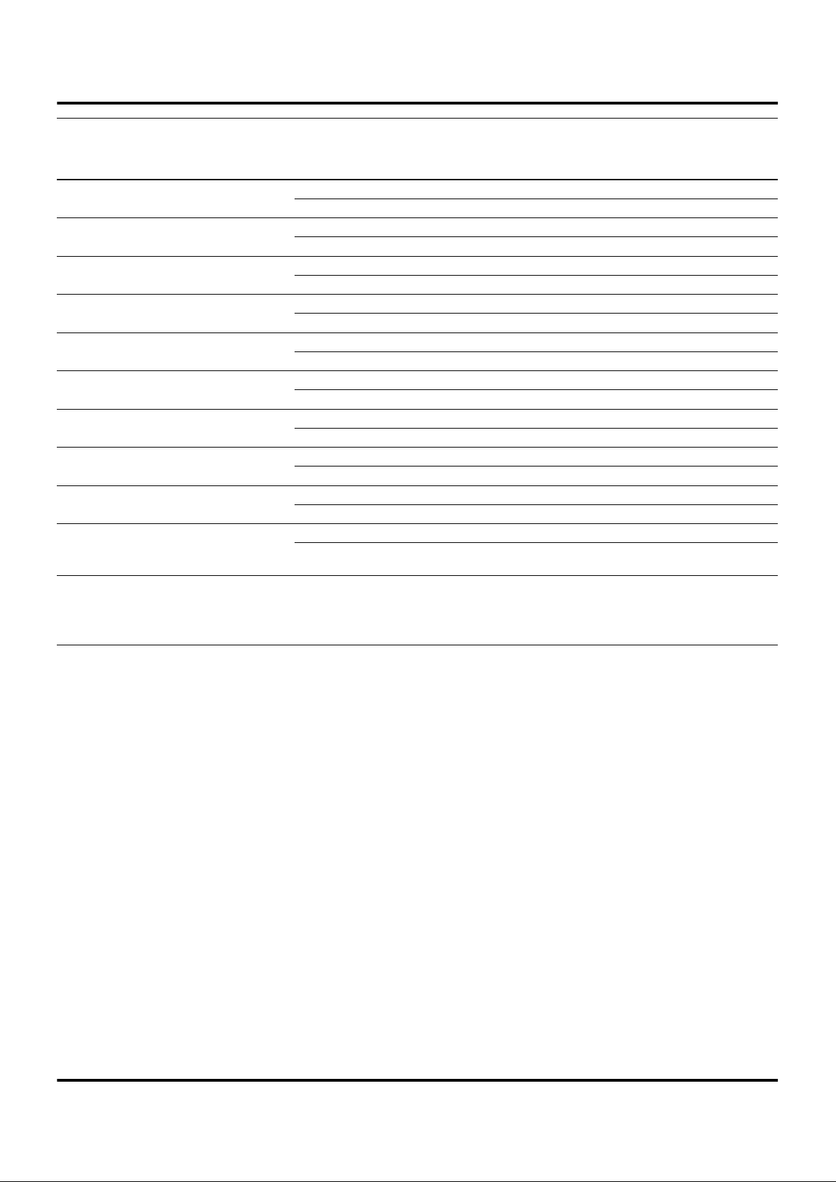
Port 0 (P02-P00). Port 0 is a 3-bit I/O, bidirectional,
Schmitt-triggered CMOS compatible I/O port. These three
I/O lines can be configured under software control to be all
inputs or all outputs (Figure 7).
Figure 6. Port 0 Configuration
Open
Out
In
1.5 2.3 Hysteresis
PAD
Port 0 (I/O)
Z86E04
and
Z86E08
Auto Latch Option
R 500 kΩ
VCC @ 5.0V
Z86C04/C08
CMOS 8-Bit Low-Cost 1K/2K-ROM Microcontrollers Zilog
19 P R E L I M I N A R Y DS97DZ80502
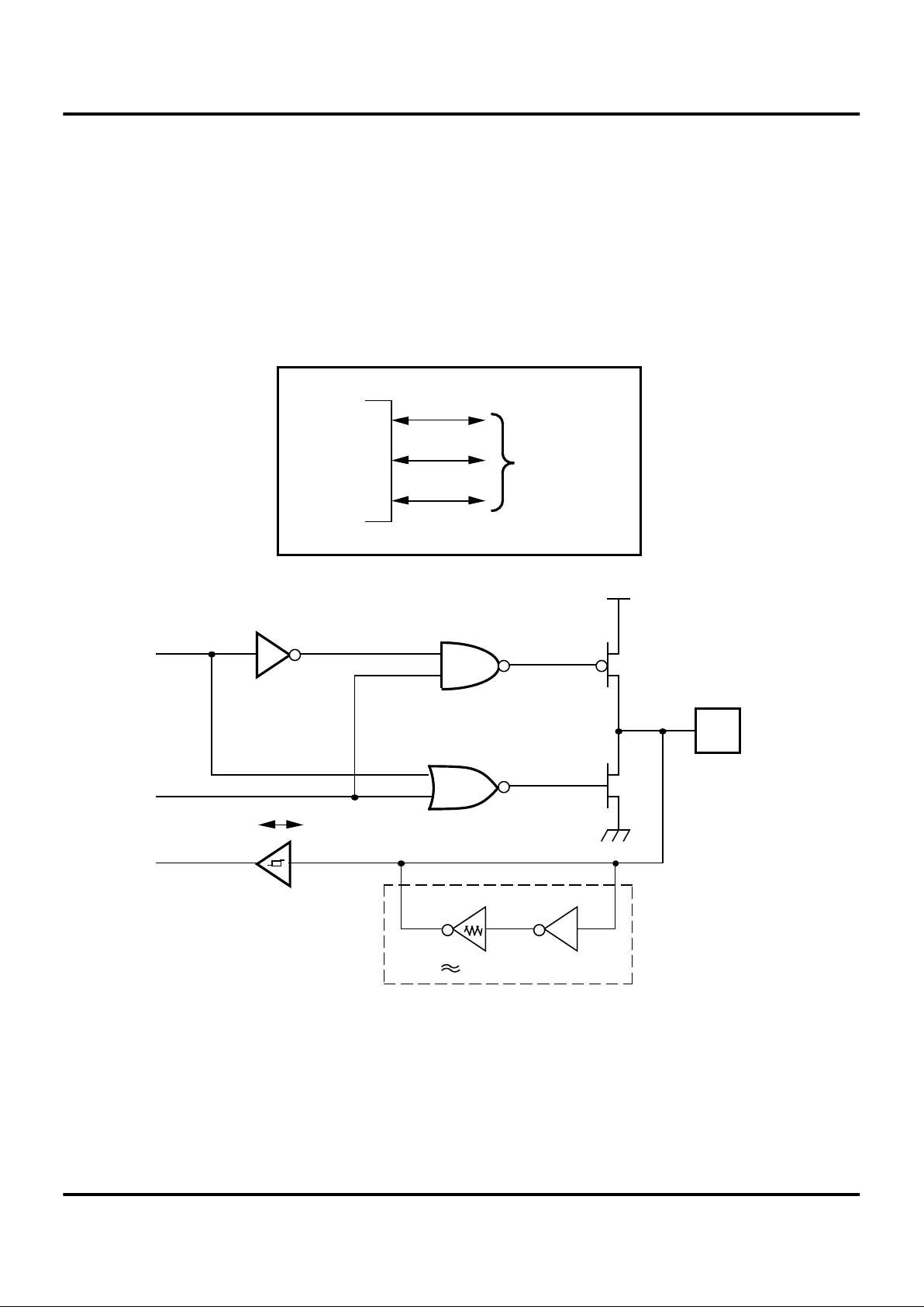
Port 2 (P27-P20). Port 2 is an 8-bit I/O, bit programmable,
bi-directional, Schmitt-triggered CMOS compatible I/O
port. These eight I/O lines can be configured under soft-
ware control to be an input or output, independently. Bits
programmed as outputs may be globally programmed as
either push-pull or open-drain (Figure 8).
Figure 7. Port 2 Configuration
Port 2 (I/O)
MCU
Open
Out
In
PAD
Open Drain
Auto Latch
R 500 kΩ
1.5 2.3 Hysteresis Vcc @ 5.0V
Z86C04/C08
CMOS 8-Bit Low-Cost 1K/2K-ROM Microcontrollers Zilog
20 P R E L I M I N A R Y DS97DZ80502
PIN DESCRIPTION (Continued)
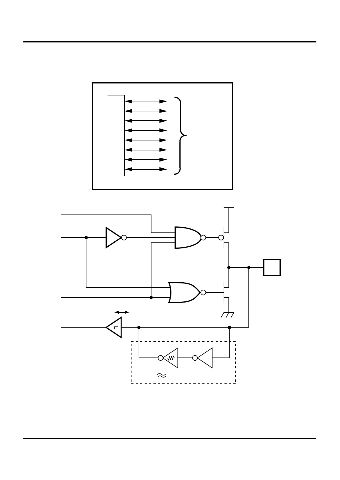
Port 3 (P33-P31). Port 3 is a 3-bit, Schmitt-triggered
CMOS compatible port with three fixed input (P33-P31)
lines. These three input lines can be configured under soft-
ware control as digital inputs or analog inputs. These three
input lines can also be used as the interrupt sources IRQ0IRQ3 and as the timer input signal (TIN) (Figure 9).
Comparator Inputs. Two analog comparators are added to
Port 3 inputs for interface flexibility. Typical applications for
these on-board comparators are: Zero crossing detection,
A/D conversion, voltage scaling, and threshold detection.
The dual comparator (common inverting terminal) features
a single power supply which discontinues power in STOP
mode. The common voltage range is 0-4V when the V
CC
is
5.0V.
Interrupts are generated on either edge of Comparator 2’s
output, or on the falling edge of Comparator 1’s output.
The comparator output may be used for interrupt generation, Port 3 data inputs, or TIN through P31. Alternately, the
comparators may be disabled, freeing the reference input
(P33) for use as IRQ1 and/or P33 input.
Figure 8. Port 3 Configuration
D1
R247 = P3M
P31 (AN1)
P32 (AN2)
1 = Analog
0 = Digital
P31
Data Latch
IRQ, Tin
DIG.
AN.
+
-
+
-
Port 3
MCU
IRQ3
P32
Data Latch
IRQ0
Vcc
P33
Data Latch
IRQ1
IRQ 0,1,2 = Falling Edge Detection
IRQ 3 = Rising Edge Detection
PAD
PAD
PAD
P33 (REF)
Z86C04/C08
Zilog CMOS 8-Bit Low-Cost 1K/2K-ROM Microcontrollers
DS97DZ80502 P R E L I M I N A R Y 21
1
FUNCTIONAL DESCRIPTION
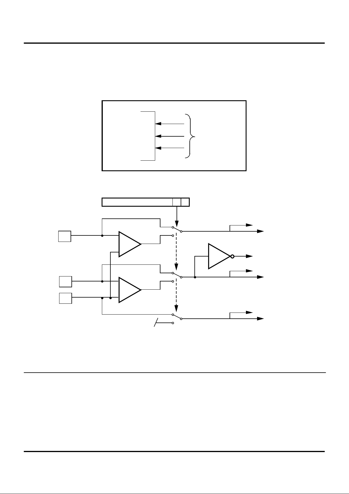
RESET. Upon power-up the Power-On Reset circuit waits
for T
POR
ms, plus 18 clock cycles, and then starts program
execution at address%000C (Hex) (Figure 10). The device
control registers’ reset value is shown in Table 2.
Figure 9. Internal Reset Configuration
Table 1. Z86C04/C08 & C05/C07 Control Registers
Reset Condition
Addr. Reg. D7 D6 D5 D4 D3 D2 D1 D0 Comments
03H (3)* Port 3 U UUUU U U U
02H (2)* Port 2 U UUUU U U U
00H (0)* Port 0 U UUUU U U U
FFH(255) SPL 0 0000 0 0 0
FFH (254) GPR 0 0000 0 0 0
FDH (253) RP 0 0000 0 0 0
FCH (252) FLAGS U UUUU U U U
FBH (251) IMR 0 UUUU U U U
FAH (250) IRQ U U 0 0 0 0 0 0 IRQ3 is used
for positive
edge detection
F9H (249) IPR U UUUU U U U
F8H (248)* P01M U U U 0 U U 0 1
F7H (247)* P3M U UUUU U 0 0
F6H (246)* P2M 1 1111 1 1 1 Inputs after
reset
F5H (245) PRE0 U UUUU U U 0
F4H (244) T0 U UUUU U U U
F3H (243) PRE1 U UUUU U 0 0
F2H (242) T1 U UUUU U U U
F1H (241) TMR 0 0000 0 0 0
Note: *Registers are not reset after a STOP-Mode Recovery using P27 pin.
A subsequent reset will cause these control registers to be re-configured as shown in
Table 2 and the user must avoid bus contention on the port pins or it may affect device reliability.
POR
(Cold Start)
P27
(Stop Mode)
Delay Line
T
POR
ms
18 CLK
Reset Filter
Chip
Reset
XTAL OSC
INT OSC
Z86C04/C08
CMOS 8-Bit Low-Cost 1K/2K-ROM Microcontrollers Zilog
22 P R E L I M I N A R Y DS97DZ80502
FUNCTIONAL DESCRIPTION (Continued)
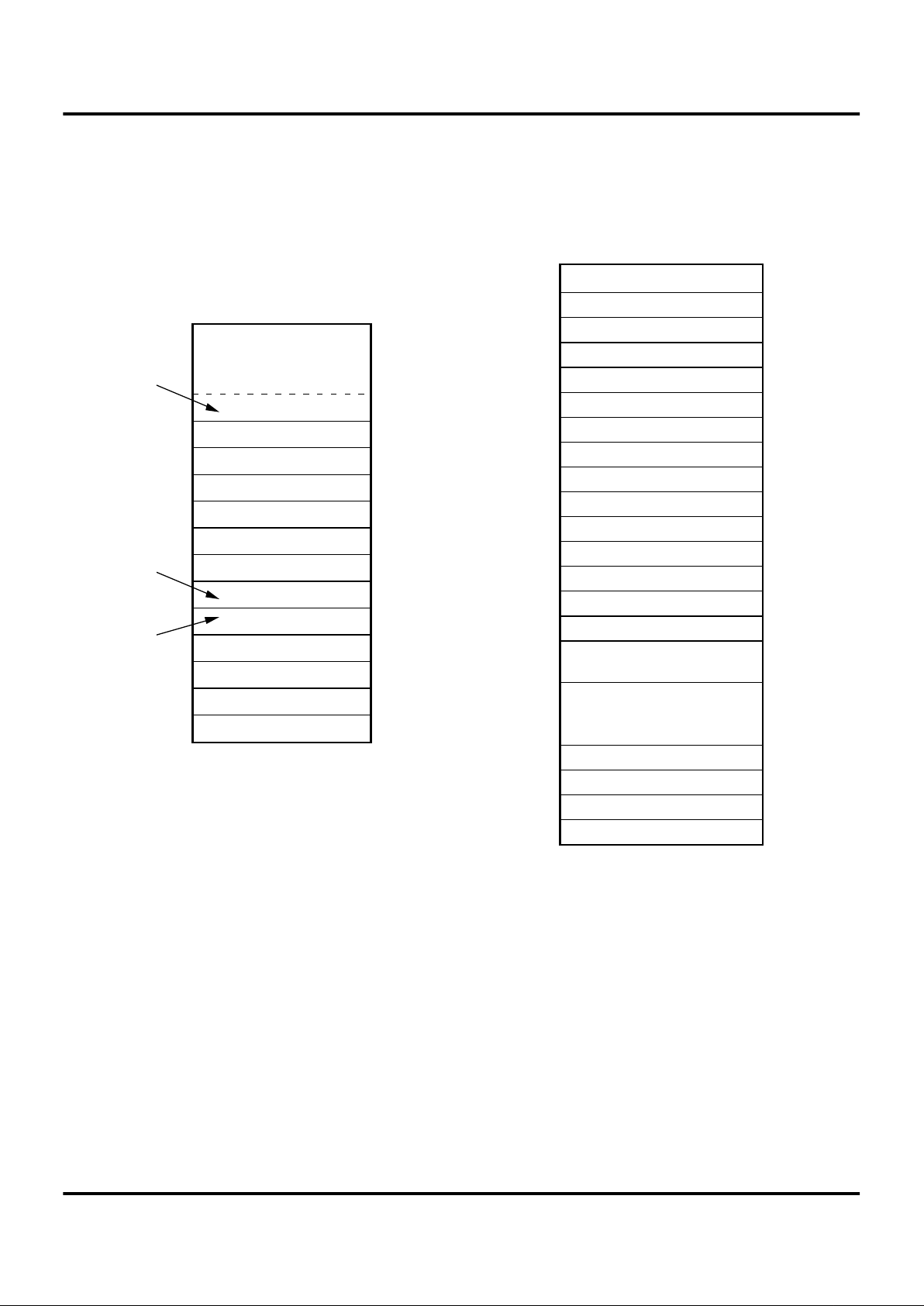
Program Memory. The Z86C04/C08 can address up to
1K/2K bytes of internal program memory (Figure 11). The
first 12 bytes of program memory are reserved for the interrupt vectors. These locations contain six 16-bit vectors
that correspond to the six available interrupts. Bytes 01023/2047 are on-chip mask-programmed ROM.
Register File. The Register File consists of three I/O port
registers, 125 general-purpose registers, and 14 control
and status registers (R0, R2-R3, R4-R127, and R241R255, respectively; see Figure 12). Note that R254 is
available for general purpose use. The Z8 instructions can
access registers directly or indirectly through an 8-bit address field. This allows short 4-bit register addressing using the Register Pointer. In the 4-bit mode, the register file
is divided into eight working register groups, each occupying 16 continuous locations. The Register Pointer (Figure
13) addresses the starting location of the active working-
register group. Upon power-up, the general purpose registers are undefined.
Figure 10. Program Memory Map
12
11
10
9
8
7
6
5
4
3
2
1
0
On-Chip
ROM
Location of
First Byte of
Instruction
Executed
After RESET
Interrupt
Vector
(Lower Byte)
Interrupt
Vector
(Upper Byte)
IRQ5
IRQ4
IRQ4
IRQ3
IRQ3
IRQ2
IRQ2
IRQ1
IRQ1
IRQ0
IRQ0
IRQ5
1023/2047
3FH/7FFH
0CH
0BH
09H
08H
07H
06H
05H
04H
03H
02H
01H
00H
0AH
Figure 11. Register File
SPL
Stack Pointer (Bits 7-0)
Reserved
Register Pointer
Program Control Flags
Interrupt Mask Register
Interrupt Request Register
Interrupt Priority Register
Ports 0-1 Mode
Port 3 Mode
Port 2 Mode
To Prescaler
Timer/Counter0
T1 Prescaler
Timer/Counter1
Timer Mode
Not Implemented
General Purpose
Registers
Port 3
Port 2
Reserved
Port 0
RP
IMR
IRQ
IPR
P3M
P2M
PRE0
T0
PRE1
T1
TMR
P3
P2
P1
P0
P01M
Flags
IndentifiersLocation
255
254
253
252
251
250
249
248
247
246
245
244
243
242
241
240
4
3
2
1
0
128
127
Z86C04/C08
Zilog CMOS 8-Bit Low-Cost 1K/2K-ROM Microcontrollers
DS97DZ80502 P R E L I M I N A R Y 23
1
Stack Pointer. The Z8 has an 8-bit Stack Pointer (R255)
used for the internal stack that resides within the 124 general-purpose registers.
General-Purpose Register (GPR). The general-purpose
register upon device power-up is undefined. The generalpurpose register upon a STOP-Mode Recovery and reset
stays in its last state. It may not keep its last state from a
VLV reset if the VCC drops below 2.6V. Note: Register R254
has been designated as a general-purpose register and is
set to 00H after any reset.
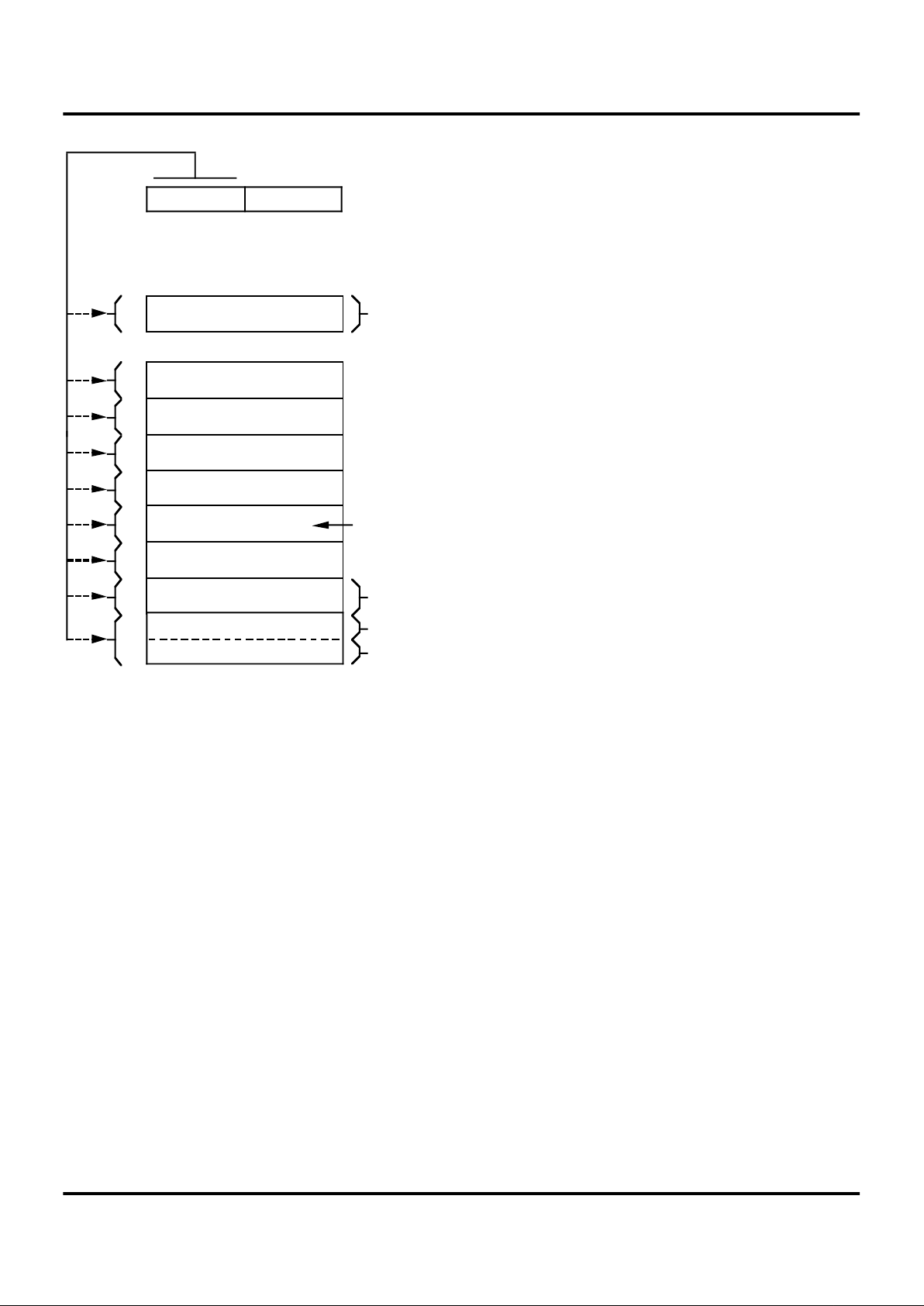
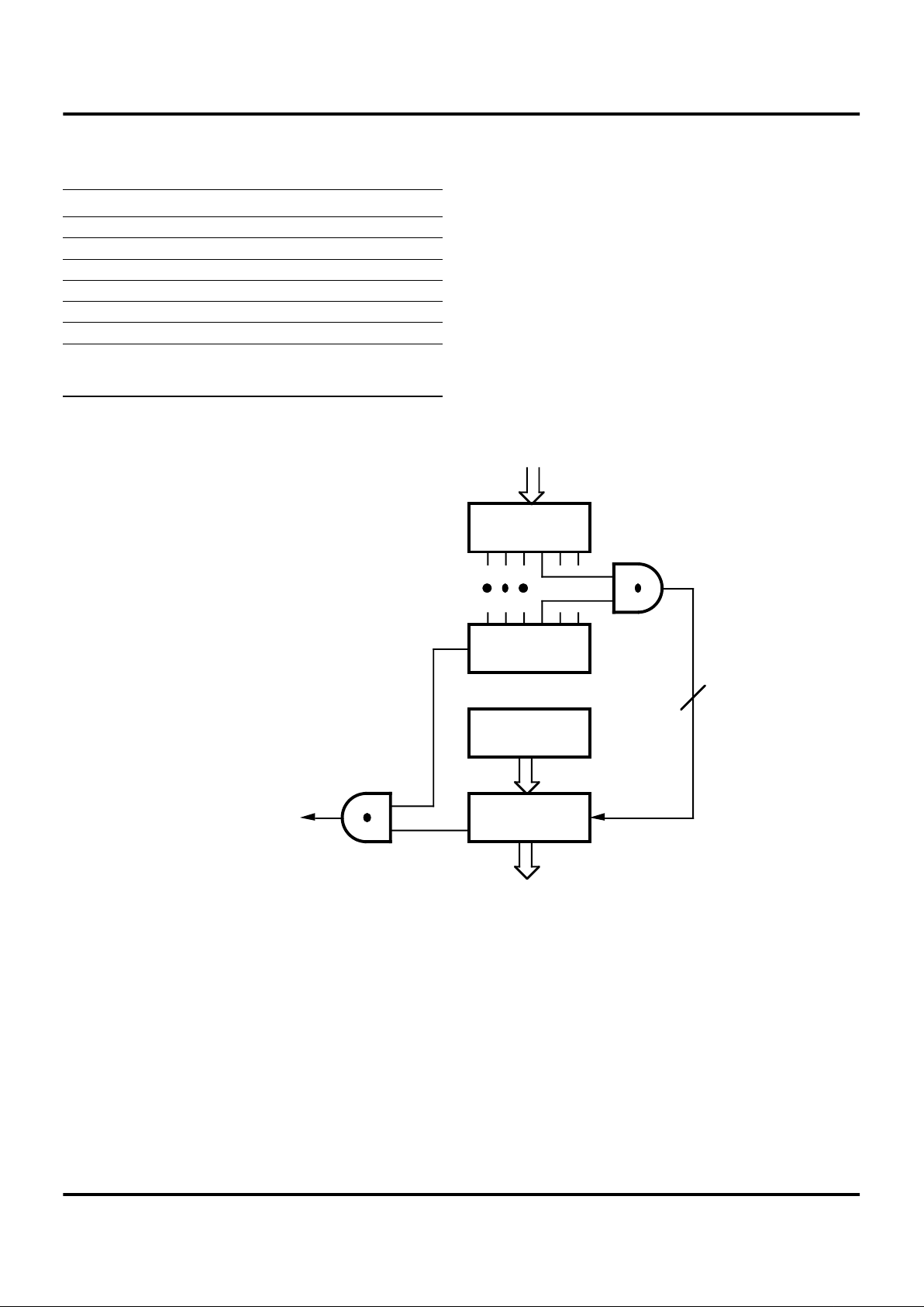
Counter/Timer. There are two 8-bit programmable
counter/timers (T0 and T1), each driven by its own 6-bit
programmable prescaler. The T1 prescaler can be driven
by internal or external clock sources, however the T0 can
be driven by the internal clock source only (Figure 14).
The 6-bit prescalers can divide the input frequency of the
clock source by any integer number from 1 to 64. Each
prescaler drives its counter, which decrements the value
(1 to 256) that has been loaded into the counter. When
both counter and prescaler reach the end of count, a timer
interrupt request, IRQ4 (T0) or IRQ5 (T1), is generated.
The counter can be programmed to start, stop, restart to
continue, or restart from the initial value. The counters can
also be programmed to stop upon reaching zero (single
pass mode) or to automatically reload the initial value and
continue counting (modulo-n continuous mode).
The counters, but not the prescalers are read at any time
without disturbing their value or count mode. The clock
source for T1 is user-definable and can be either the internal microprocessor clock divided by four, or an external
signal input through Port 3. The Timer Mode register configures the external timer input (P31) as an external clock,
a trigger input that is retriggerable or non-retriggerable, or
as a gate input for the internal clock.
Figure 12. Register Pointer
The upper nibble of the register file address
provided by the register pointer specifies
the active working-register group.
r7 r6 r5 r4 R253
(Register Pointer)
I/O Ports
Specified Working
Register Group
The lower nibble
of the register
file address
provided by the
instruction points
to the specified
register.
r3 r2 r1 r0
Register Group 1
Register Group 0
R15 to R0
Register Group F
R15 to R4*
R3 to R0
R15 to R0
FF
F0
0F
00
1F
10
2F
20
3F
30
4F
40
5F
50
6F
60
7F
70
*Expanded Register Group (0) is selected in this figure
by handling bits D3 to D0 as "0" in Register R253(RP).
Z86C04/C08
CMOS 8-Bit Low-Cost 1K/2K-ROM Microcontrollers Zilog
24 P R E L I M I N A R Y DS97DZ80502
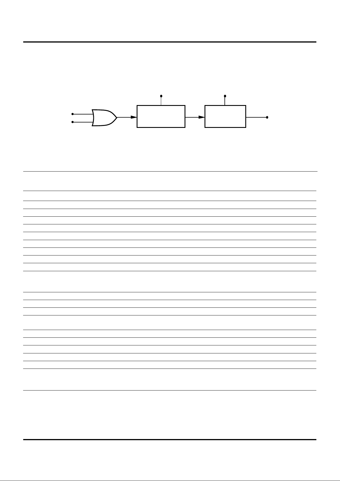
Interrupts. The Z8 has six interrupts from six different
sources. These interrupts are maskable and prioritized
(Figure 15). The six sources are divided as follows: the falling edge of P31 (AN1), P32 (AN2), P33 (REF), the rising
edge of P32 (AN2), and the two counter/timers. The Interrupt Mask Register globally or individually enables or disables the six interrupt requests (Table 3).
When more than one interrupt is pending, priorities are resolved by a programmable priority encoder that is controlled by the Interrupt Priority register. All Z8 interrupts are
vectored through locations in program memory. When an
Interrupt machine cycle is activated, an interrupt request is
granted. This disables all subsequent interrupts, saves the
Program Counter and Status Flags, and then branches to
the program memory vector location reserved for that interrupt. This memory location and the next byte contain the
16-bit starting address of the interrupt service routine for
that particular interrupt request.
To accommodate polled interrupt systems, interrupt inputs
are masked and the interrupt request register is polled to
determine which of the interrupt requests needs service.
Note: User must select any Z86C08 mode in Zilog’s C12
ICEBOX
™
emulator. The rising edge interrupt is not
supported on the Z86CCP00ZEM emulator.
Figure 13. Counter/Timers Block Diagram
OSC
PRE0
Initial Value
Register
T0
Initial Value
Register
T0
Current Value
Register
6-Bit
Down
Counter
8-Bit
Down
Counter
÷ 2
÷4
6-Bit
Down
Counter
8-Bit
Down
Counter
PRE1
Initial Value
Register
T1
Initial Value
Register
T1
Current Value
Register
Clock
Logic
IRQ4
IRQ5
Internal Data Bus
Write
Write
Read
Internal Clock
Gated Clock
Triggered Clock
External Trigger
T P31
Write Write Read
Internal Data Bus
Internal
Clock
÷4
IN
*
*
Note: Divide-by-two is not used in Low EMI Mode.
Z86C04/C08
CMOS 8-Bit Low-Cost 1K/2K-ROM Microcontrollers Zilog
25 P R E L I M I N A R Y DS97DZ80502
FUNCTIONAL DESCRIPTION (Continued)
Table 2. Interrupt Types, Sources, and Vectors
Name Source Vector Location Comments
IRQ0 AN2(P32) 0,1 External (F) Edge
IRQ1 REF(P33) 2,3 External (F) Edge
IRQ2 AN1(P31) 4,5 External (F) Edge
IRQ3 AN2(P32) 6,7 External (R) Edge
IRQ4 T0 8,9 Internal
IRQ5 T1 10,11 Internal
Notes:
F = Falling edge triggered
R = Rising edge triggered.
Figure 14. Interrupt Block Diagram
IRQ
IMR
IPR
PRIORITY
LOGIC
6
Global
Interrupt
Enable
Vector Select
Interrupt
Request
IRQ0 - IRQ5

Z86C04/C08
CMOS 8-Bit Low-Cost 1K/2K-ROM Microcontrollers Zilog
26 P R E L I M I N A R Y DS97DZ80502
Clock. The on-chip oscillator has a high-gain, parallel-res-
onant amplifier for connection to a RC, crystal, ceramic
resonator, LC, or any suitable external clock source
(XTAL1 = Input, XTAL2 = Output). The crystal should be
AT cut, 12 MHz max, with a series resistance (RS) less
than or equal to 100 Ohms.
The crystal should be connected across XTAL1 and
XTAL2 using the vendor’s crystal recommended capacitors (which depends on the crystal manufacturer, ceramic
resonator and PCB layout) from each pin directly to device
Ground pin 14 (Figure 16).
Note that the crystal capacitor loads should be connected
to V
SS
pin 14 to reduce ground noise injection.
To use 32 KHz crystal, the 32 KHz operational mask option
must be selected, and an external resistor R must be connected across XTAL1 and XTAL2.To use RC oscillator,
the RC oscillator option must be selected.
HALT Mode. This instruction turns off the internal CPU
clock but not the crystal oscillation. The counter/timers and
external interrupts IRQ0, IRQ1, IRQ2, and IRQ3 remain
active. The device can be recovered by interrupts, either
externally or internally generated. An interrupt request
must be executed (enabled) to exit HALT mode. After the
interrupt service routine, the program continues from the
instruction after the HALT.
STOP Mode. This instruction turns off the internal clock
and external crystal oscillation and reduces the standby
current. The STOP mode can be released by two methods.
The first method is a RESET of the device by removing
VCC or dropping the VCC below VLV. The second method
is if P27 is at a low level when the device executes the
STOP instruction. A low condition on P27 releases the
STOP mode regardless if configured for input or output.
Program execution under both conditions begins at location 000C (Hex). However, when P27 is used to release
the STOP mode, the I/O port mode registers are not reconfigured to their default power-on conditions. This prevents any I/O, configured as output when the STOP instruction was executed, from glitching to an unknown
state. To use the P27 release approach with STOP mode,
use the following instruction:
Note: (X = dependent upon user’s application.)
In order to enter STOP or HALT mode, it is necessary to
first flush the instruction pipeline to avoid suspending execution in mid-instruction. To do this, the user must execute
a NOP (opcode = FFH) immediately before the appropriate
sleep instruction, that is, as follows:
Watch-Dog Timer (WDT). The Watch-Dog Timer is enabled by instruction WDT. When the WDT is enabled, it
cannot be stopped by the instruction. With the WDT instruction, the WDT should be refreshed once the WDT is
enabled within every Twdt period; otherwise, the Z8 resets
itself. The WDT instruction affects the Flags accordingly: Z
= 1, S = 0, V = 0.
WDT = 5F (Hex)
LD P2M, #1XXX XXXXB
NOP
STOP
FF NOP ; clear the pipeline
6F STOP ; enter STOP mode
or
FF NOP ; clear the pipeline
7F HALT ; enter HALT mode
Figure 15. Oscillator Configuration
XTAL1
XTAL2
C1
C2
C1
C2
Ceramic
Resonator
or Crystal
External Clock
L
LC Clock
XTAL1
XTAL2
XTAL1
XTAL2
*
*
*
*
*
= Use pin 14.
XTAL1
XTAL2
C1
C2
R
32 KHz
32 KHz Crystal Clock
XTAL1
XTAL2
R
RC Clock
C
*
*
*

Z86C04/C08
Zilog CMOS 8-Bit Low-Cost 1K/2K-ROM Microcontrollers
DS97DZ80502 P R E L I M I N A R Y 27
1
Opcode WDT (5FH). The first time opcode 5FH is execut-
ed, the WDT is enabled, and subsequent execution clears
the WDT counter. This has to be done within the maximum
T
WDT
period; otherwise, the WDT times out and generates
a Reset. The generated Reset is the same as a Power-On
Reset of T
POR
plus 18 XTAL clock cycles. The WDT does
not work (run) in STOP mode. The WDT is disabled during
and after a Reset, until the WDT is enabled again.
Opcode WDH (4FH). When this instruction is executed it
will enable the WDT during HALT. If not, the WDT will stop
when entering HALT. This instruction does not clear the
counters, it facilitates running the WDT function during
HALT mode. A WDH instruction executed without executing WDT (5FH) has no effect.
Permanent WDT Mask Option. Only when the
Permanent WDT Mask Option is selected, then the WDT
is hardwired to be enabled after reset. The WDT will
operate in Run mode, HALT mode, and STOP mode. The
Opcode 5FH is used to refresh or clear the WDT counter.
The WDH instruction (4FH) has no effect The WDT will not
run in Stop Mode if the system clock driving the WDT is
selected (Z86C04 only).
System Clock Driving WDT Mask Option (Z86C04 only)
When this option is selected, the Z8’s system clock drives
the WDT instead of the on-board RC oscillator driving the
WDT. The WDT time-out will be SCLK x 32,512.The WDT
will not run in Stop Mode.
Note: The internal clock frequency is one-half the external
clock frequency in standard mode.
The device will function normally at or above 3.0V under all
conditions. Below 3.0V, the device functions normally until
the Low Voltage Protection trip point (V
LV
) is reached. The
device is guaranteed to function normally at supply
voltages above the low voltage trip point for the
temperatures and operating frequencies in Cases 1 and 2.
The actual low voltage trip point is a function of
temperature and process parameters (Figure 17).
ROM Protect. ROM Protect fully protects the Z86C04/C08
ROM code from being read internally. When ROM Protect
is selected. ROM look-up tables can be used in this
mode.
Low V oltage Protection (V
LV
). Maximum (VLV) Conditions:
Case 1: TA= –40°C , +85°C , Internal Clock
Frequency equal or less than 6 MHz
Case 2: T
A
= –40°C , +105°C , Internal Clock
Frequency equal or less than 4 MHz
2 MHz (Typical)
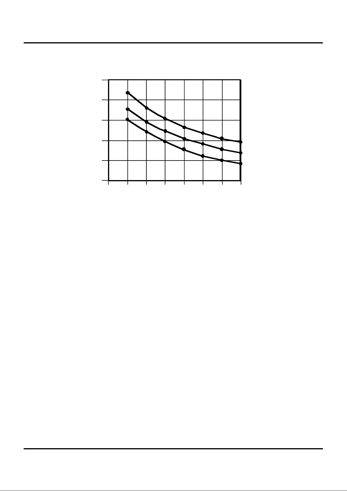
Temp –40C° 0°C +25°C +70°C +105°C
V
LV
3.0 2.75 2.6 2.3 2.1
Figure 16. Typical Z86C04/C08 VLV vs. Temperature
V
CC
(Volts)
3.2
2.8
2.6
2.4
2.2
2.0
-60 -40 -20 0 20 40 60 80 100 120 140
3.0
Temperature (°C)
VLV (Typical)

Z86C04/C08
CMOS 8-Bit Low-Cost 1K/2K-ROM Microcontrollers Zilog
28 P R E L I M I N A R Y DS97DZ80502
Z8® CONTROL REGISTER DIAGRAMS
Figure 17. Timer Mode Register (F1H: Read/Write)
Figure 18. Counter Time 1 Register (F2H: Read/Write)
Figure 19. Prescaler 1 Register (F3H: Write Only)
D7 D6 D5 D4 D3 D2 D1 D0
0 Disable T Count
1 Enable T Count
0 No Function
1 Load T
0
0
0
0 No Function
1 Load T
1
0 Disable T Count
1 Enable T Count
1
1
T Modes
00 External Clock Input
01 Gate Input
10 Trigger Input
(Non-retriggerable)
11 Trigger Input
(Retriggerable)
IN
R241 TMR
Reserved (Must be 0.)
D7 D6 D5 D4 D3 D2 D1 D0
T Initial Value
(When Written)
(Range 1-256 Decimal
01-00 HEX)
T Current Value
(When READ)
1
1
R242 T1
D7 D6 D5 D4 D3 D2 D1 D0
Count Mode
0 T Single Pass
1 T Modulo
1
1
Clock Source
1 T Internal
0 T External Timing Input
(T ) Mode
IN
1
1
Prescaler Modulo
(Range: 1-64 Decimal
01-00 HEX)
R243 PRE1
Figure 20. Counter/Timer 0 Register (F4H: Read/Write)
Figure 21. Prescaler 0 Register (F5H: Write Only)
Figure 22. Port 2 Mode Register (F6H: Write Only)
Figure 23. Port 3 Mode Register (F7
H
: Write Only)
D7 D6 D5 D4 D3 D2 D1 D0
T Initial Value
(When Written)
(Range: 1-256 Decimal
01-00 HEX)
T Current Value
(When READ)
0
0
R244 T0
D7 D6 D5 D4 D3 D2 D1 D0
Count Mode
0 T0 Single Pass
1 T
0
Modulo-n
Reserved (Must be 0.)
Prescaler Modulo
(Range: 1-64 Decimal
01-00 Hex)
R245 PRE0
D7 D6 D5 D4 D3 D2 D1 D0
P2 - P2 I/O Definition
0 Defines Bit as OUTPUT
1 Defines Bit as INPUT
70
R246 P2M
D7 D6 D5 D4 D3 D2 D1 D0
0 Port 2 Open-Drain
1 Port 2 Push-Pull Active
Port 3 Inputs
0 Digital
1 Analog
Reserved (Must be 0.)
R247 P3M

Z86C04/C08
Zilog CMOS 8-Bit Low-Cost 1K/2K-ROM Microcontrollers
DS97DZ80502 P R E L I M I N A R Y 29
1
Figure 24. Port 0 and 1 Mode Register
(F8H: Write Only)
Figure 25. Interrupt Priority Register (F9
H
: Write Only)
Figure 26. Interrupt Request Register (FA
H
:
Read/Write)
D7 D6 D5 D4 D3 D2 D1 D0
P0 - P0 Mode
00 = Output
01 = Input
Reserved (Must be 0.)
Must be 1.
R248 P01M
03
D7 D6 D5 D4 D3 D2 D1 D0
Interrupt Group Priority
000 Reserved
001 C > A > B
010 A > B > C
011 A > C > B
100 B > C > A
101 C > B > A
110 B > A > C
111 Reserved
IRQ3, IRQ5 Priority (Group A)
0 IRQ5 > IRQ3
1 IRQ3 > IRQ5
IRQ0, IRQ2 Priority (Group B)
0 IRQ2 > IRQ0
1 IRQ0 > IRQ2
IRQ1, IRQ4 Priority (Group C)
0 IRQ1 > IRQ4
1 IRQ4 > IRQ1
Reserved (Must be 0.)
R249 IPR
D7 D6 D5 D4 D3 D2 D1 D0
IRQ0 = P32 Input ↓
IRQ1 = P33 Input ↓
IRQ2 = P31 Input ↓
IRQ3 = P32 Input ↑
IRQ4 = T0
IRQ5 = T1
Reserved (Must be 0.)
R250 IRQ
Figure 27. Interrupt Mask Register (FBH: Read/Write)
Figure 28. Flag Register (FCH: Read/Write)
Figure 29. Register Pointer (FD
H
: Read/Write)
Figure 30. Stack Pointer (FFH: Read/Write)
D7 D6 D5 D4 D3 D2 D1 D0
Reserved (Must be 0.)
1 Enables IRQ5-IRQ0
(D = IRQ0)
1 Enables Interrupts
0
R251 IMR
D7 D6 D5 D4 D3 D2 D1 D0
User Flag F1
User Flag F2
Half Carry Flag
Decimal Adjust Flag
Overflow Flag
Sign Flag
Zero Flag
Carry Flag
R252 Flags
D7 D6 D5 D4 D3 D2 D1 D0
Reserved (Must be 0.)
Register Pointer
R253 RP
D7 D6 D5 D4 D3 D2 D1 D0
Stack Pointer Lower
Byte (SP - SP )
7 0
R255 SPL

Z86C04/C08
CMOS 8-Bit Low-Cost 1K/2K-ROM Microcontrollers Zilog
30 P R E L I M I N A R Y DS97DZ80502
DEVICE CHARACTERISTICS
Standard Mode
Figure 31. VIL, VOL vs. Temperature
1.0
.5
1.5
2.0
2.5
3.0
3.5
4.0
4.5
5.0
5.5
6.0
-20 0 406080
5.5V
3.0V
5.5V
3.0V
Vcc (Volt)
V
V
Temp
(C )
100-60 -40 20 120
OL
IL

Z86C04/C08
Zilog CMOS 8-Bit Low-Cost 1K/2K-ROM Microcontrollers
DS97DZ80502 P R E L I M I N A R Y 31
1
Standard Mode
Figure 32. VIH, VOH vs. Temperature
1.0
1.5
2.0
2.5
3.0
3.5
4.0
4.5
5.0
5.5
6.0
-20 0 40 60 80
5.5V
3.0V
3.0V
Vcc (Volt)
V Vs Temp
V Vs Temp
100
-60
-40 20 120
5.5V
OH
IH
Temp
C
Figure 33. Typical IOH vs. V
OH
-7.0
-8.0
-6.0
-5.0
-4.0
-3.0
0
-2.0
I
(mA)
OH
2.0 3.0 4.0 5.0 6.0 V
(Volt
)
OH
3.0V
5.5V
125
25
-40 C
125 25
-40 C
Z86C04/C08
CMOS 8-Bit Low-Cost 1K/2K-ROM Microcontrollers Zilog
32 P R E L I M I N A R Y DS97DZ80502
Figure 34. Typical WDT Time Out Period vs. V
CC
Over Temperature
-40°C
10
20
30
40
2.5 3.0 3.5 4.0 4.5 5.0 5.5 6.0
Voltage
+25°C
+105
°
C
Time
(ms)
0
Z86C04/C08
Zilog CMOS 8-Bit Low-Cost 1K/2K-ROM Microcontrollers
DS97DZ80502 P R E L I M I N A R Y 33
1
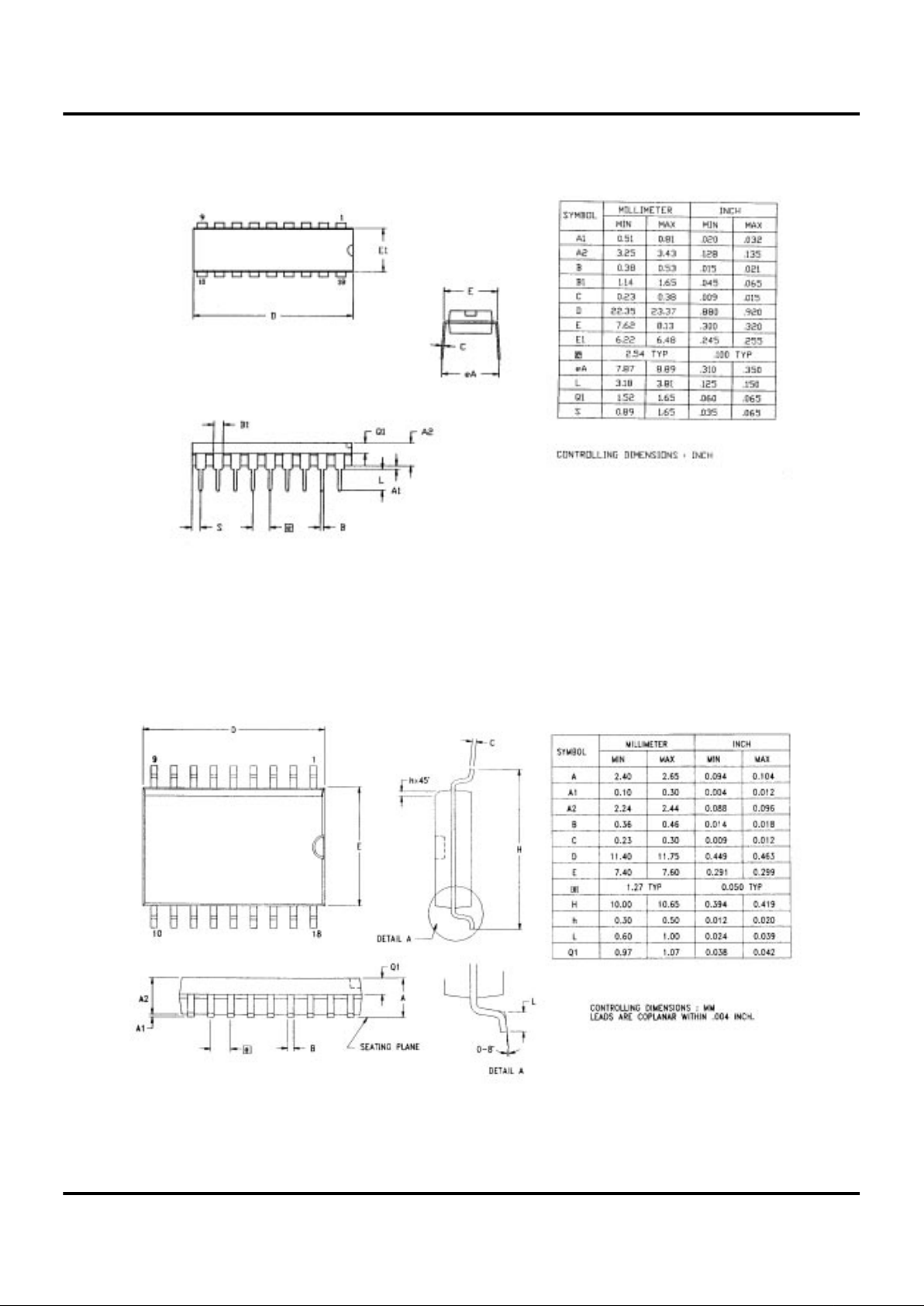
PACKAGE INFORMATION
Figure 35. 18-Pin DIP Package Diagram
Figure 36. 18-Pin SOIC Package Diagram

Z86C04/C08
CMOS 8-Bit Low-Cost 1K/2K-ROM Microcontrollers Zilog
34 P R E L I M I N A R Y DS97DZ80502
ORDERING INFORMATION
For fast results, contact your local Zilog sale offices for assistance in ordering the part(s) desired.
CODES
Preferred Package
P = DIP
S = SOIC
Preferred Temperature
S = 0°C to +70°C
Longer Lead Time
E = –40°C to +105°C
A = -40°C to +125°C
Speeds
12 = 12 MHz
Environmental
C = Plastic Standard
Z86C04
(12 MHz)
Standard Temperature
Z86C08
(12 MHz)
Standard Temperature
18-Pin DIP 18-Pin SOIC 18-Pin DIP 18-Pin SOIC
Z86C0412PSC Z86C0412SSC Z86C0812PSC Z86C0812SSC
Extended Temperature Extended Temperature
18-Pin DIP 18-Pin SOIC 18-Pin DIP 18-Pin SOIC
Z86C0412PEC
Z86C0412PAC
Z86C0412SEC
Z86C0412SAC
Z86C0812PEC
Z86C0812PAC
Z86C0812SEC
Z86C0812SAC
Example:
Z 86C04 12 P S C
Environmental Flow
Temperature
Package
Speed
Product Number
Zilog Prefix
is a Z86C04, 12 MHz, DIP, 0°C to +70°C, Plastic Standard Flow
 Loading...