


GENERAL DESCRIPTION
PRELIMINARY
P
RELIMINARY
C
USTOMER PROCUREMENT SPECIFICATION
Z86228
LINE 21 CLOSED CAPTION
CONTROLLER (L21C)
CPS DC-4243-00
Z86228
The Z86228 (Line 21 Closed-Caption Controller) is a single
I.C. designed to provide the functional performance of a
L21C Decoder module. This Superintegration™ VLSI device
is completely self contained requiring only composite
video, a horizontal timing signal as input and an external
keyer (i.e., video switch between TV video and ClosedCaption video) to produce captioned video. The Z86228
uses a wired logic approach to perform the functions
selected through its input control signals. It is fabricated
using standard CMOS technology and designed to achieve
the lowest possible cost.
The Z86228 is intended for use in a set-top decoder or in
any television receiver conforming to the NTSC standard.
It is capable of processing and displaying all standard
L21C format transmissions including the codes specified
by the FCC "Report and Order" on GEN Docket No. 91-1,
dated April 12, 1991. In addition, the device conforms to
the Electronic Industry Association's Recomended Practice
608, which provides supplemental guidelines for the
transmission of captions, text, and Extended Data Services
(EDS) on NTSC Field 2. Extended Data Services (EDS)
packets encoded on Field 2 , may be displayed in either of
two screen formats. If and when PAL and SECAM TV
standards define a protocol using the Line 21 format, this
design will be readily convertible to that standard.
The Line 21 Closed Captioning System
The L21C system provides for the transmission of CAPTION
information and other TEXT material as an encoded
composite data signal. This is during the unblanked portion
of Line 21, field 1, of the standard NTSC video signal. The
video signal conforms to the Standard Synchronizing
Waveform for Color Transmission given in Sub-part E, Part
73 of the FCC Rules and Regulations.
DC-4243-00 (2-18-94)
1
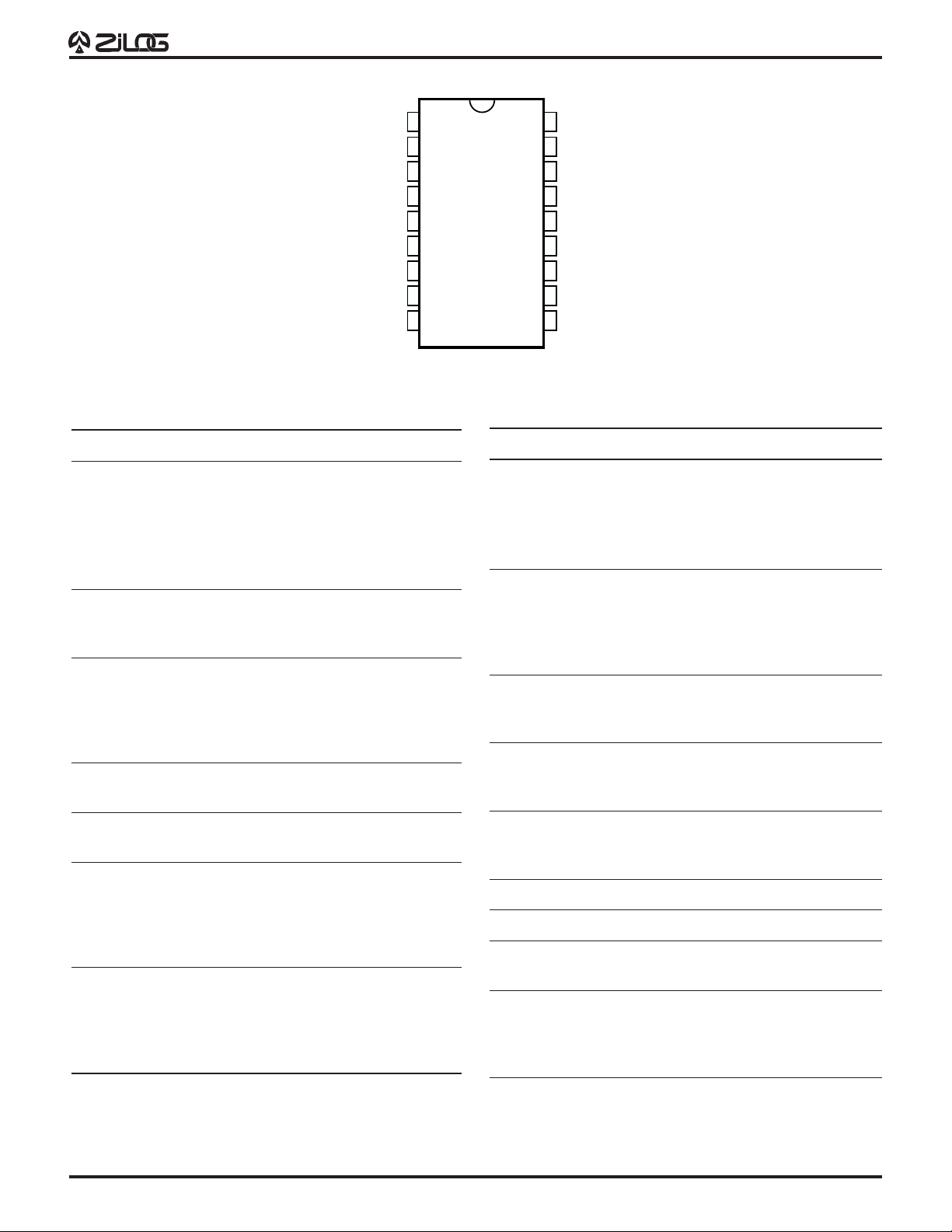
PIN DESCRIPTION
PRELIMINARY
CPS DC-4243-00
Z86228
DONF/SEN
NRESET
VSS (Digital)
Pin No. Signal Description
11 Composite Video Input (CVI)
Composite NTSC video, nominally 1.0V p-p,.
band limited to 600 kHz. Circuit operates with
signal variations between 0.7-1.4V p-p. It is
recommended that this signal pin be driven by
an emitter follower through a 0.1 µF capacitor.
12 Sync Slice Level (SSL)
Capacitor (0.1µF) to store sync slice level
voltage.
8 H Flyback Input (HFI)
Horizontal sync input at CMOS levels, polarity
independent. Typically derived from the H
Flyback pulse or any other horizontal timing
signal.
13 H Loop Filter (HLF)
Value to be specified
18
17
16
15
14
13
12
11
10
LNG/SCK
CT/SDA
NSIN
VDD (Digital)
VDD (Analog)
HLF
SSL
CVI
VSS (Analog)
BOX
LUM
HFI
1
2
3
4
R
5
G
6
B
7
8
9
18-Pin DIP Package Diagram
Pin No. Signal Description
2 NRESET
Master reset for the I.C. and must be used in the
Parallel Control Mode. It may be tied High in the
Serial Mode if reset is to be performed through
the serial data stream.
18 LAG/SCK Input (control)
In Parallel Mode this input selects the Data
Channel to be processed (along with CT). CMOS
input High=LANGUAGE I, Low=LANGUAGE II.
In Serial Mode this input is Serial Clock In.
3 Box Output (Box)
Active High, CMOS level “black box” keying
signal for Caption/Text display area.
4 Luminance Output (LUM)
Active High, CMOS level signal.
Character video luminance signal.
9V
(Digital) Digital Ground
SS
Connect to system ground
1 DONF/SEN Input (control)
In Parallel Mode this input controls the Decoder
On/Off function CMOS input with High = On,
Low = Off. In Serial Mode this input is the Enable
for serial data input.
17 CT/SDA Input (control)
In Parallel Mode this input selects the Data
Channel to be processed (along with LNG).
CMOS input with High=CAPTIONS, Low =TEXT.
In Serial mode this input is serial data input.
2
5, 6, 7 Color signals, RGB Outputs
Active High, CMOS level color character video
for color receiver use.
15 V
14 V
10 V
Digital Power pin. Connect to +5V source.
DD
Analog
DD
Analog. Analog Ground. Connect to
SS
system ground.
16 (NSIN) Input (Control)
Selects the mode to be used in interpreting the
signals on the three Control pins. High = Parallel
Mode, Low = Serial Mode.
Horizontal Timing
PRELIMINARY
CPS DC-4243-00
Z86228
The timing of the output signals; Box, Luminance, and RGB
is set so that the start of the leading box preceding the first
displayable character cell will occur at 13.6*µs. (*Value
may be altered by a Mask change - consult factory.) This
is after the midpoint of the leading edge of the horizontal
sync pulse of the composite video signal measured at pin
11 of the Z86228. It is assumed that the delay through the
low pass filter will be 220 ns (refererence Figure).
There are two ways to execute a FULL RESET of the
Z86228:
1. Hold NRESET Low for 100 ns. This stops all internal
circuits. The part is static and the 100 ns is the worst
case time for the NRESET signal to propagate through
the various gates.
ABSOLUTE MAXIMUM RATINGS
Sym Description Min Max Units
V
cc
T
STG
T
A
Notes:
* Voltages on all pins with respect to GND.
Supply Voltage* –0.3 +7.0 V
Storage Temp –65°C +150° C
Oper Ambient Temp 0° 70° C
2. Send NRESET command through the serial interface.
The result is the same as in number 1.
FULL RESET is useful during power-up. A FULL RESET of
the part during normal operation is not necessary.
A partial reset may also be executed through the serial
interface only. This is the COMMAND PROCESSOR RESET.
Basically, all internal timing circuits continue to operate,
but the caption display is removed from the screen and the
Z86228 waits for new line 21 data. This is useful for
situations such as channel change.
Stress greater than those listed under Absolute Maximum
Ratings may cause permanent damage to the device. This
is a stress rating only; operation of the device at any
condition above those indicated in the operational sections
of these specifications is not implied. Exposure to absolute
maximum rating conditions for an extended period may
affect device reliability.
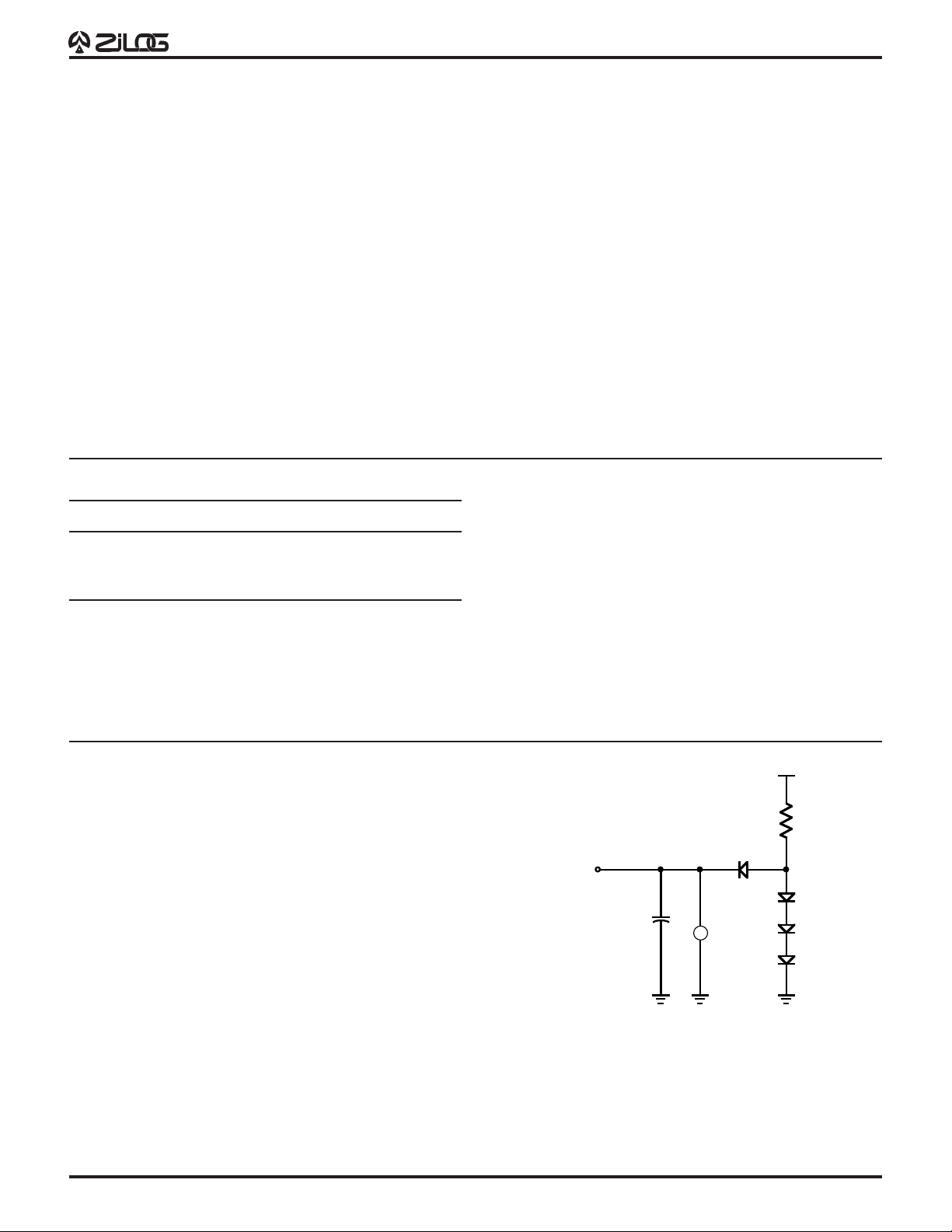
STANDARD TEST CONDITIONS
The characteristics listed below apply for standard test
conditions as noted. All voltages are referenced to GND.
Positive current flows into the referenced pin in Standard
Test Load.
From Output
Under Test
+5V
2.1 kΩ
150 pF
▼ 250 µA
Standard Test Load
3

PRELIMINARY
DC CHARACTERISTICS
TA = 0°C to +70°C; VCC = +4.75V to +5.25V
Sym Parameter Min Max Units Conditions
CPS DC-4243-00
Z86228
V
IL
V
IH
V
OL
V
OH
I
IL
I
CC
Notes:
[1] Pin 13 (HLF)
[2] Pin 17 (CT/SDA) is Open-Drain.
[3] VDD Digital + VDD Analog combined.
Input Voltage Low 0 0.2V
Input Voltage High 0.7V
Output Voltage Low 0.4 V IOL = 1.00 mA
Output Voltage High VCC–0.4 V IOH = 0.75 mA [2]
Input Leakage –.0 3.0 µA 0V, V
Supply Current 25 mA [3]
AC AND TIMING CHARACTERISTICS*
(Reference Line 21 AC/DC Timing)
Composite Video Input
Amplitude: 1.0 V p-p, ±3 dB
Polarity: Sync tips negative
Bandwidth 600 kHz
Horizontal Signal Input (preferably H Flyback)
Amplitude: CMOS level signal, Low ≤ 0.2VCC, High ≥ 0.7V
Polarity: Any
Frequency: 15,734.263 Hz, ± 3%
CC
CC
V
CC
1V I
CC
V
V
= 50 µA [1]
OL
CC
Line 211 Input Parameters (at 1.0 V p-p)
Code Level: 50 IRE ± 10 IRE
Clock Run-in Start 2: 10.5 µs, ±0.5µs
Input Signal-to-Random Noise Performance
Unit will function down to a 25 dB ratio (CCIR weighted) with one error per row or better at that level.
Internal Sync Circuits
The internal sync circuits will lock to all 525 line signals having a vertical sync pulse that meets the following conditions:
■ It is at least 2.5H long.
■ It starts at the proper 2H boundary for its field.
■ If equalizing pulse serrations are present they must be less than 0.125H in width.
Timing Signals
Dot Clock: 768 x FH = 12.0839 MHz
Dot Period: 82.75 nsec
Character Cell Width: 1.324 µsec
Width of Row (Box): 45.018 µsec
Width of Row (Char): 42.370 µsec
*All values are nominal and not fully characterized.
4

AC/DC TIMING
Line 21
PRELIMINARY
Center of Active Video
CPS DC-4243-00
Z86228
Log Ref
"white"
Blanking 0 IRE
-40 IRE
-100 IRE
Comp Video
A
LOW
PASS
FILTER
13.6µs
Cell Width = 1.324 µs
-(100) IRE
1st CHAR
2nd CHAR
CHAR LUM = 42.370 µs
BOX = 45.018 µs
35.73µs
1
Z86228
LUM
BOX
R
G
B
32nd CHAR
-(0) IRE
-(40) IRE
Line 21 AC/DC Timing
5

PRELIMINARY
AC CHARACTERISTICS
TA = 0°C to + 70°C; VCC = +4.75V to +5.25V
CPS DC-4243-00
Z86228
SEN
SCK
SDA
Tckd
Tout Toff
HI-Z
SS-OUT D0-IN D(1-7)-IN A0-IN
Tckl Tenl
Tckh
Tdsu
Tdh
HI-Z
HI-Z
Tout ToffTasu Tah
SS-OUT
Serial Mode Timing Diagram
Symbol Description Min. Max. Units
T
OUT
T
OFF
T
CKD
T
CKL
T
CKH
T
DSU
T
DH
T
ENI
T
ASU
T
AH
Output enable time, ENA rising edge to Data Out 200 ns
Output disable time, CLK or ENA falling edge to Data Hi-Z 100 ns
Data read time, ENA rising edge to CLK low 200 ns
CLK low time 200 ns
CLK high time 200 ns
Data set-up time 100 ns
Data hold time 100 ms
ENA low time 200 ns
A0 set-up time 100 ns
A0 hold time 100 ns
HI-Z
6

PRELIMINARY
Low Margin:
Customer is advised that this product does not meet
Zilog's internal guardbanded test policies for the
specifcation requested and is supplied on an exception
basis. Customer is cautioned that delivery may be uncertain
and that, in addition to all other limitations on Zilog liability
Pre-Characterization Product:
The product represented by this CPS is newly introduced
and Zilog has not completed the full characterization of the
product. The CPS states what Zilog knows about this
product at this time, but additional features or non-
CPS DC-4243-00
Z86228
stated on the front and back of the slaes order
acknowledgement, Zilog makes no claim as to quality and
reliability under the CPS. The product remains subject to
standard warranty for replacement due to defects in
materials and workmanship.
conformance with some aspects of the CPS may be found,
either by Zilog or its customers in the course of further
application and characterization work. In addition, Zilog
cautions that delivery may be uncertain at times, due to
start-up yield issues.
© 1994 by Zilog, Inc. All rights reserved. No part of this document
may be copied or reproduced in any form or by any means
without the prior written consent of Zilog, Inc. The information in
this document is subject to change without notice. Devices sold
by Zilog, Inc. are covered by warranty and patent indemnification
provisions appearing in Zilog, Inc. Terms and Conditions of Sale
only. Zilog, Inc. makes no warranty, express, statutory, implied or
by description, regarding the information set forth herein or
regarding the freedom of the described devices from intellectual
property infringement. Zilog, Inc. makes no warranty of merchantability or fitness for any purpose. Zilog, Inc. shall not be
responsible for any errors that may appear in this document.
Zilog, Inc. makes no commitment to update or keep current the
information contained in this document.
Zilog’s products are not authorized for use as critical components in life support devices or systems unless a specific written
agreement pertaining to such intended use is executed between
the customer and Zilog prior to use. Life support devices or
systems are those which are intended for surgical implantation
into the body, or which sustains life whose failure to perform,
when properly used in accordance with instructions for use
provided in the labeling, can be reasonably expected to result in
significant injury to the user.
Zilog, Inc. 210 East Hacienda Ave.
Campbell, CA 95008-6600
Telephone (408) 370-8000
Telex 910-338-7621
FAX 408 370-8056
7
 Loading...