

Datasheet Z8613112PSC, Z8613112SSC, Z8612912PSC, Z8612912SSC, Z8613012PSC Datasheet (ZILOG)
...
1
P
RELIMINARY
P
RODUCT
S
PECIFICATION
Z86129/130/131
NTSC L
INE
21 D
ECODER
1
FEATURES
Speed Pin Count/ Standard On-Screen Display Automatic Data Extraction
Devices (MHz) Package Types Temp. Range & Closed Captioning V-Chip Time of Day
Z86129 12 18-Pin DIP, SOIC 0 ° to +70 ° C Yes Yes Yes
Z86130 12 18-Pin DIP, SOIC 0 ° to +70 ° C No Yes Yes
Z86131 12 18-Pin DIP, SOIC 0 ° to +70 ° CNo NoYes
■
Complete Stand-Alone Line 21 Decoder for ClosedCaptions and Extended Data Services (XDS).
■
Preprogrammed to Provide Full Compliance with EIA608 Specifications for Extended Data Services.
■
Automatic Extraction and Serial Output of Special
XDS Packets such as Time of Day, Local Time Zone,
and Program Rating ( V-Chip ).
■
Cost-Effective Solution for NTSC Violence Blocking
inside Picture-in-Picture (PiP) Windows.
■
Minimal Communications and Control Overhead
Provides Simple Implementation of Violence Block,
Closed Caption, and Auto Clock Set Features.
■
Programmable, Full Screen On-Screen Display (OSD)
for Creating OSD or Captions inside a Picture-inPicture (PiP) Window (Z86129 only).
2
■
I
C Serial Data and Control Communication
■
User-Programmable Horizontal Display Position for
easy OSD Centering and Adjustment (Z86129 only).
GENERAL DESCRIPTION
The Z86129/130/131 is a stand-alone integrated circuit,
capable of processing Vertical Blanking Interval (VBI) data
from both fields of the video frame in data conforming to
the transmission format defined in the Television Decoder
Circuits Act of 1990 and in accordance with the Electronics
Industry Association specification 608 (EIA-608).
The Line 21 data stream can consist of data from several
data channels multiplexed together. Field 1 has four data
channels, two Captions and two Text. Field 2 has five
additional data channels, two Captions, two Text and
Extended Data Services (XDS). XDS data structure is
defined in EIA-608. The Z86129 can recover and display
data transmitted on any of these nine data channels. The
Z86130 and Z86131 are derivatives of the Z86129 which
can recover XDS data and output the recovered data via
the serial port. The Z86130 and Z86131 do not have OSD
DS96TEL0200 1
capability, but are ideally suited for Line 21 data slicer
applications.
The Z86129/130/131 can recover and output to a host
processor via the I
defined in EIA-608. On-chip XDS filters are fully
programmable, enabling recovery of only those XDS data
packets selected by the user, making the Z86129/130 an
ideal choice for implementing NTSC Violence Block. The
Z86131 is designed especially for extracting XDS time
information for Automatic Clock-Set features in TVs,
VCRs, and Set-Top boxes.
In addition, the Z86129/130 is ideally suited to monitor Line
21 of video displayed in a PiP window for violence blocking
purposes. A block diagram of the Z86129/130/131 is
shown in Figure 1.
2
C serial bus any XDS data packet
Z86129/130/131
NTSC Line 21 Decoder P R E L I M I N A R Y
GENERAL DESCRIPTION (Continued)
+5V
6 4 15 14 1613
VDD
12
SDO
SDA
SCK
Serial
SEN
SMS
Intro
VIN/
Data Line
Data CLK
Data
Sliced
Data
Buffer
Addr Bus
Row
Status Reg
Control Port
VW
Data Bus
FEW
Recovery
AW
Slicer
SIG
Lock
Command
Test Reg
II Lock
Digital
PG
Processor
4
Row
Slicer
SYNC
Address
10
Latch
MUX
6
DOT CLK
RAM
Display
DIV
DOT CLK
V Lock
COMP SYNC
DEC
ADDR
Character
13
8
Latch
Display
FLD
CIR
CHAR
CW
CHAR CLK
OSCO/S
ADDR
Decoder
Generator
4
SS CTR
MSGR
Logic
Output
Line &
LS
FLD
Control
I Drive
& MUX
Field
Control
SLS
SFLD
CKT
POR
V/I
Ref
Line & Fld
RED
GREEN
BLUE
BOX
10
Decodes
11
1
9
17 3 2 18
Z86129 only
RREF
Vss(A)
Vss
Loop
LPF
Filter
FR
HIN
5
7
Video
Dual
Clamp
Slice Level
8
CSYNC
CG Lines
CG
Logic
MSYNC
PH1
PH2
Figure 1. Z86129 Block Diagram
2 DS96TEL0200
1
PIN DESCRIPTION
V
GREEN*
BLUE*
SEN
SMS
VIDEO
CSYNC
SS
HIN
LPF
*Z86129 Only
1
2
3
4
5
6
7
8
9
Figure 2. Z86129/130/131, 18-Pin DIP/SOIC
Pin Configuration
18
17
16
15
14
13
12
11
10
RED*
BOX*
SDO
SCK
SDA
VIN/INTRO
V
DD
VSS(A)
RREF
°
°
Z86129/130/131
P R E L I M I N A R Y NTSC Line 21 Decoder
Table 1. 18-Pin DIP and SOIC Pin Identification
No. Symbol Function Direction
1V
SS
Power Supply GND
2* GREEN Video Output Output
3* BLUE Video Output Output
4 SEN Serial Enable Input
5 HIN Horizontal In Input
6 SMS Serial Mode Select Input
7 VIDEO Composite Video Input
8 CSYNC Composite Sync Output
9 LPF Loop Filter Output
10 RREF Resistor Reference Input
11 V
12 V
(A) Pwr. Supply (Analog) GND
SS
DD
Power Supply
13 VIN/INTRO Vertical In/Interrupt Out In/Output
14 SDA Serial Data In/Output
15 SCK Serial Clock Input
16 SDO Serial Data Out Output
17* BOX OSD Timing Signal Output
18* RED Video Output Output
Note: DIP and SOIC pin configuration are identical. *However,
the Z86130/Z86131 do not have signals on pins 2, 3, 18 and 19.
ABSOLUTE MAXIMUM RATINGS
Symbol Parameter Value Unit
V
DD
V
IN
V
OUT
I
IN
I
OUT
I
DD
P
D
T
STG
T
L
Notes:
Voltages referenced to V
Maximum ratings are those values beyond which damage to the device may occur.
Functional operation should be restricted to the limits specified in the DC and AC Characteristics tables or Pin Description section.
DC Supply Voltage –0.5 to 6.0 V
DC Input Voltage –0.5 to V
DC Output Voltage –0.5 to V
+0.5 V
DD
+0.5 V
DD
CAUTION: DC Input Current per Pin +10 mA
DC Output Current per Pin +20 mA
DC Supply Current +30 mA
Power Dissipation per Device 300 mW
Storage Temperature –65 to +150
Lead Temperature, 1 mm from Case for 10 seconds 260
(A) and V
SS
SS
.
C
C
DS96TEL0200 3
Z86129/130/131
NTSC Line 21 Decoder P R E L I M I N A R Y
STANDARD TEST CONDITIONS
µ
The characteristics listed below apply for standard test
+5V
conditions as noted. All voltages are referenced to
Ground. Positive current flows into the referenced pin
(Figure 3).
From Output
Under Test
150 pF
250 µA
2.1 kΩ
Figure 3. Standard Test Load
DC ELECTRICAL CHARACTERISTICS
Note: T
Symbol Parameter Conditions Min. Max. Unit
Note: *Not guaranteed
= 0 ° C to +70 ° C; V
A
V
IL
V
IH
V
OL
V
OH
I
IL
I
DD
K φ
I
LP
= +4.75V to +5.25V
DD
Input V oltage Low 0 0.2 V
Input V oltage High 0.7 V
Output V oltage Low I
Output V oltage High I
Input Leakage 0V, V
= 1.00 mA – 0.4 V
OL
= 0.75 mA V
OH
DD
–0.4V – V
DD
–3.0 3.0
DD
V
DD
DD
V
V
Supply Current Estimated* 30 mA
VCO Gain – TBD MHz/V
Loop Filter Current – TBD mA
A
AC AND TIMING CHARACTERISTICS
Composite Video Input
Parameter Conditions
Amplitude 1.0V p-p ± 3 dB
Polarity Sync tips negative
Bandwidth 600 kHz
Signal Type Interlaced
Max Input R 470 ohms
DC Offset Signal to be AC coupled with a minimum series capacitance of 0.1 µ F
4 DS96TEL0200

P R E L I M I N A R Y NTSC Line 21 Decoder
1
ELECTRICAL CHARACTERISTICS
Non Standard Video Signals must have the following characteristics:
Z86129/130/131
Parameter Conditions
Sync Amplitude 200 mV minimum
Vertical Pulse Width 3H ± 0.5H
Vertical Pulse Tilt 20 mV maximum
H Timing Phase Step (Head Switch) ± 10 µ s maximum
Fh Deviation (long term) ± 0.5% maximum
Fh p-p Deviation (short term) ± 0.3% maximum
Vertical Sync Signal The internal sync circuits will lock to all 525 or 625 line signals having a vertical
sync pulse that meets the following conditions:
1. It is at least 2H wide.
2. It starts at the proper 2H boundary for its field.
3. If equalizing pulse serrations are present, they must be less than 0.125H in
width.
Minimum Signal-to-Noise The Z86129/130/131 will function down to a 25 dB signal-to-noise ratio (CCIR
weighted) with one error per row or better at that level.
Ratio to Composite Video Input
Horizontal Signal Input (preferably H Flyback)
Parameter Conditions
Amplitude CMOS level signal where Low <= 0.2 V
Video Lock Mode: Polarity
Frequency
HIN Lock Mode: Polarity
Frequency
Any
15,734.263 Hz ± 3%
Any
Same as Display Horizontal Flyback Pulse (HFB) pulse
CC
Line 21 Input Parameters (at 1.0V p-p)
Note: Line 21 must be in its proper position to the leading edge of the Vertical Sync signal.
Parameter Conditions
Cod Amplitude 50 IRE
Code Zero Level 5 IRE, +15 IRE relative to Back Porch
Start of Code 10.5 ±0.5 µs, (Measured from the midpoint of the falling edge of the last cloc k run-in cycle
to the midpoint of the rising edge of the start bit.)
Start of Data 3.972 µs, –0.00 µsec, +0.30 µs (Measured from the midpoint of the falling edge of the last
clock run-in cycle to the midpoint of the rising edge of the start bit.
Timing Signals
Parameter Conditions
Dot 768 x FH = 12.0839 MHz
Dot Period 82.75 ns
Character Cell Width 1.324 µs (tH/48)
Width of Row (Box) 45.018 µs (34 chars = 17/24 x tH
Width of Row (Char) 42.370 µs (32 chars = 2/3 x tH
Horizontal Display Timing The timing of the output signals Box and RGB have been set to make a centered display.
The positioning of these outputs can be adjusted in 330 ns increments by writing a new
value to the Z86129 H Position Register (Address = 02h).
DS96TEL0200 5

Z86129/130/131
NTSC Line 21 Decoder P R E L I M I N A R Y
PIN DESCRIPTIONS
Inputs
VIDEO (Pin 7). Composite NTSC video input, 1.0V p-p
(nom), band limited to 600 kHz. Circuit will operate with
signal variation between 0.7-1.4V p-p. The polarity is sync
tips negative. This signal pin should be AC coupled
through a 0.1 µF capacitor and driven by a source
impedance of 470 ohms or less.
HIN (Pin 5). Horizontal sync input at CMOS levels. When
the device is used in the VIDEO LOCK mode, this signal
pulls the on-chip VCO within the proper range. The circuit
uses the frequency of this signal which must be within ±3%
Fh but can be of either polarity. When used in the H LOCK
mode, the VCO phase locks to the rising edge of this
signal. The HPOL bit of the H Position register can be set
to operate with either polarity of input signal. This is usually
the H Flyback signal. The timing difference between HIN
rising edge and the leading edge of composite sync (of
VIDEO input) is one of the factors which will affect the
horizontal position of the display. Any shift resulting from
the timing of this signal can be compensated for with the
horizontal timing value in H Position Register.
SMS (Pin 6). Mode select pin for the Serial Control Port.
When this input is at a CMOS High state (1) the Serial
Control Port will operate in the SPI mode. When the input
is Low (0), the Serial Control Port will operate in the I
slave mode. In SPI mode, the SEN pin must be tied High.
(See Reset Operation section.)
2
Input/Output
VIN/INTRO (Pin 13). In external (EXT) vertical lock mode
of operation, the internal vertical sync circuits will lock to
the VIN input signal applied at this pin. The part will lock to
the rising or falling edge of the signal in accordance with
the setting of the V Polarity command. The default is rising
edge. The VIN pulse must be at least 2 lines wide.
In INTRO Mode, when configured for internal vertical
synchronization, this pin will be an output pin providing an
interrupt signal to the master control device in accordance
with the settings in the Interrupt Mask Register.
SDA (Pin 14). When the Serial Control Port has been set
2
C mode operation, this pin serves as the bidirectional
to I
data line for sending and receiving serial data. In SPI mode
operation it operates as serial data input. SPI mode output
data is available on the SDO pin.
Outputs
SDO (Pin 16). Provides the serial data output when SPI
mode communications have been selected. This pin is not
used in I2C mode operation.
Box (Pin 17*). Black box keying output is an active High,
CMOS level signal used to key in the black box in the
C
captions/text displays. This output will be in the highimpedance state when the background attribute has been
set to semi-transparent (*Z86129 only).
SEN (Pin 4). Enable signal for the SPI mode operation of
the Serial Control Port. When this pin is Low (0), the SPI
port is disabled and the SDO pin is in the high-impedance
state. Transitions on the SCK and SDA pins are ignored.
SPI mode operation is enabled when SMS is High (1).
SCK (Pin 15). Input pin for serial clock signal from the
master control device. In I2C mode operation the clock rate
is expected to be within I2C limits. In SPI mode, the
maximum clock frequency is 10 MHz.
Reset Operation. When the SMS and SEN pins are both
in the Low (0) state, the part will be in the Reset state.
Therefore, in the I2C mode the SEN pin can be used as an
NReset input. When SPI mode is used, if three wire
operation is desired, both SMS and SEN can be tied
together and used as the NReset input. In either mode,
NReset must be held Low (0) for at least 100 ns.
RED, GREEN, BLUE (Pins 2*, 3*, 18*). Positive acting
CMOS levels signals (*Z86129 only).
Color Mode: Red, Green and Blue character video outputs
for use in a color receiver.
■ Mono Mode: All three outputs carry the character
luminance information.
Notes: The selection of Color/Mono Mode is user
controlled in bit D1 of the Configuration Register
(Address=00h). (See Internal Registers section.).
6 DS96TEL0200

Z86129/130/131
1
P R E L I M I N A R Y NTSC Line 21 Decoder
Pins With External Components
CSync (Pin 8). Sync slice level. A 0.1 µF capacitor must
be tied between this pin and analog ground VSS(A). This
capacitor stores the sync slice level voltage.
LPF (Pin 9). Loop Filter. A series RC low-pass filter must
be tied between this pin and analog ground VSS(A). There
must also be second capacitor from the pin to VSS(A).
Values for the three parts to be specified at a later date.
RREF (Pin 10). Reference setting resistor. Resistor must
be 10 kohms, ±2%.
Z86129/130/131 BLOCK DIAGRAM DESCRIPTION
The Z86129 is designed to process both fields of Line 21
of the television VBI and provide the functional
performance of a Line 21 Closed-Caption decoder and
Extended Data Service decoder. It requires two input
signals, Composite Video and a horizontal timing signal
(HIN), and several passive components for proper
operation. A vertical input signal is also required if OSD
display mode is desired when no video signal is present.
The Decoder performs several functions, namely
extraction of the data from Line 21, separation of the
normal Line 21 data from the XDS data, on-screen display
(Z86129 only) of the selected data channel and outputting
of the XDS data through the serial communications
channel.
Input Signals
The Composite Video input should be a signal which is
nominally 1.0 Volt p-p with sync tips negative and band
limited to 600 kHz. The Z86129 will operate with an input
level variation of ±3 dB.
The HIN input signal is required to bring the VCO close to
the desired operating frequency. It must be a CMOS level
signal. The HIN signal can have positive or negative
polarity and is only required to be within 3% of the standard
H frequency. When configured for EXT HLK operation, this
signal should correspond to the H Flyback signal.
The timing difference between HIN rising edge and the
leading edge of composite sync (of VIDEO input) is one of
the factors that will affect the horizontal position of the
display. Any shift resulting from the timing of this signal can
be compensated for with the horizontal timing value in the
H Position register.
Video Input Signal Processing
The Comp Video input is AC coupled to the device where
the sync tip is internally clamped to a fixed reference
voltage by means of a dual clamp. Initially, the unlocked
signal is clamped using a simple clamp. Improved impulse
noise performance is then achieved after the internal sync
Power Supply
VDD (Pin 12). The voltage on this pin is nominally 5.0 Volts
and may range between 4.75 to 5.25 Volts with respect to
the VSS pins.
VSS (Pins 1, 11). These pins are the lowest potential
power pins for the analog and digital circuits. They are
normally tied to system ground. Note: The recommended
printed circuit pattern for implementing the power
connection and critical components will be supplied at a
later date.
circuits lock to the incoming signal. Noise rejection is
obtained by making the clamp operative only during the
sync tip. The clamped composite video signal is fed to both
the Data Slicer and Sync Slicer blocks.
The Data Slicer generates a clean CMOS level data signal
by slicing the signal at its midpoint. The slice level is
established on an adaptive basis during Line 21. The
resultant value is stored until the next occurrence of that
Line 21. A high level of noise immunity is achieved by
using this process.
The Sync Slicer processes the clamped Comp Video
signal to extract Comp Sync. This signal is used to lock the
internally generated sync to the incoming video when the
video lock mode of operation has been enabled. Sync
slicing is performed in two steps. In the non-locked mode,
the sync is sliced at a fixed offset level from the sync tip.
When proper lock operation has been achieved, the slice
level voltage switches from a fixed reference level to an
adaptive level. The slice level is stored on the sync slice
capacitor, CSYNC.
The Data Clock Recovery circuit operates in conjunction
with the Digital H Lock circuit. They produce a 32H clock
signal (DCLK) that is locked in phase to the clock run-in
burst portion of the sliced data obtained from the Data
Slicer. When Line 21 code appears, DCLK phase lock is
achieved during the clock run-in burst and used to reclock
the sliced data. Once phase lock is established it is
maintained until a change in video signal occurs.
The Digital H Lock circuit produces the video timing gates,
PG, STG, and so on, which are locked in phase with
HSYNC, the video timing signal, no matter which H lock
mode is used in the display generation circuits. This
independent phase lock loop is able to respond quickly to
changes in video timing, without concern for display
stability requirements.
DS96TEL0200 7

Z86129/130/131
NTSC Line 21 Decoder P R E L I M I N A R Y
Z86129/130/131 BLOCK DIAGRAM DESCRIPTION (Continued)
VCO and One Shot
All internal timing and synchronizing signals are derived
from the on-board 12 MHz VCO. Its output is the Dot Clk
signal used to drive the Horizontal and Vertical counter
chains and for display timing. The One Shot circuit
produces a horizontal timing signal derived from the
incoming video and qualified by the Copy Guard logic
circuits.
The VCO can be locked in phase to two different sources.
For television operation, where a good horizontal display
timing signal is available, the VCO is locked to the HIN
input through the action of the Phase Detector (PH2).
When a proper HIN signal is not available, such as in a
VCR, the VCO can be locked to the incoming video
through the Phase Detector (PH1). In this case the
frequency detector (FR) circuit is activated as required to
bring the VCO within the pull-in range of PH1.
Timing and Counting Circuits
The Dot Clk is first divided down to produce the character
timing clock CHAR CLK. This signal is then further divided
to generate the horizontal timing signals, H, 2H and
HSQR. These timing signals are used in the data output
(display) circuits.
The H signal is further divided in the LINE and FLD CNTR
to produce the various decodes used to establish vertical
lock and to time the display and control functions required
for proper operation. The H signal is also used to generate
the Smooth Scroll timing signal for display.
Command Processor
The Command Processor circuit controls the manipulation
of the data for storage and display. It processes the
Control Port input commands to determine the display
status desired and the data channel selected. During the
display time (lines 43-237), this information is used to
control the loading, addressing and clearing of the Display
RAM and the operations of the Character ROM and Output
Logic circuits.
During data recovery time (TV lines 21-42), the Command
Processor, in conjunction with the data recovery circuits,
recovers the XDS data and the data for the selected data
channel. Data is sent to the RAM for storage and display
and/or to the serial port, as appropriate. Where necessary,
the Command Processor converts the input data to the
appropriate form.
Output Logic (Z86129 only)
The output logic circuits operate together to generate the
output color signals RED, GREEN and BLUE and the Box
signal. When MONOchrome mode is selected all three
color outputs will carry the Luminance information. These
outputs are positive output logic signals.
The character ROM contains the dot pattern for all the
characters. The output logic provides the hardware
underline, graphics characters and the Italics slant
generator circuits. The smooth scroll display is achieved
by the smooth scroll counter logic controlling the
addressing of the Character ROM.
The V Lock circuits produce a noise free vertical pulse
derived from the horizontal timing signal. When the user
selects Video as the vertical lock source, the internal
synchronizing signals are phased up with the incoming
video by comparing the internally generated vertical pulse
to an input vertical pulse derived from the Comp Sync
signal provided by the Sync Slicer. In the vertical lock set
to VIN mode the VIN signal is used in place of the signal
derived from Comp Sync. In either case, when proper
phasing has been established, this circuit outputs the
LOCK signal which is used to provide additional noise
immunity to the slicing circuits.
The LOCKed state is established only after several
successive fields have occurred in which these two vertical
pulses remain in sync. Once LOCKed, the internal timing
will flywheel until such time as the two vertical pulses lose
coincidence for a number of consecutive fields. Until
LOCK is established, the decoder operates on a pulse for
pulse basis.
Decoder Control Circuit
The Decoder Control circuit block is the users
communications port. It converts the information provided
to the control port into the internal control signals required
to establish the operating mode of the decoder. This port
can be operated in one of two serial modes. The SMS pin
is used to establish the serial control mode to be used.
In the two wire (I2C) control mode, the Z86129/130/131 will
respond to its slave address for both the read and write
conditions. If the read bit is Low (indicating a WRITE
sequence) then the Z86129/130/131 will respond with an
acknowledge. The master should then send an address
byte followed by a data byte. If the read bit is High
(indicating a READ sequence) then the Z86129/130/131
will respond with an acknowledge followed by a status byte
then a data byte. Read data will only be available through
indirect addressing. Write addressing will have both
indirect and direct modes. The busy bit in the status byte
will indicate if the write operation has been completed or if
read data is available.
8 DS96TEL0200

Z86129/130/131
1
P R E L I M I N A R Y NTSC Line 21 Decoder
The SPI mode is a three wire bus with the Z86129/130/131
performing as the slave device. Communication is
synchronized by the SCK signal generated by the master.
Typically, the serial data output is transmitted on the falling
edge of SCK and the received data is captured on the
rising edge of SCK. All data is exchanged as 8-bit bytes.
Z86129/130/131 FUNCTIONAL DESCRIPTION
The Z86129 provides full function NTSC, Line 21
performance. Input commands are included to enable the
decoder to process and display any of the eight
Caption/Text data channels (CC1, CC2, CC3, CC4, T1,
T2, T3 or T4) contained in Line 21 of either field of the
incoming video. XDS data can also be selected for display.
The DECODER ON/OFF commands control whether or
not the Line 21 data in the selected channel is actually
displayed. When switched to the DECODER OFF (TV)
state, incoming data in the selected channel will still be
processed but not displayed.
The Z86129/130/131 can also be configured to operate
with PAL or SECAM video signals. It will decode
information encoded into its VBI in Line 22. The encoded
data must conform to the waveform and command
structure defined for NTSC Line 21 operation.
VCO Lock
The design includes a VCO with stable gain characteristics
and good power supply rejection. The internal horizontal
and vertical synchronizing circuits provide a high degree of
noise immunity. There are options for both horizontal and
vertical lock. The VCO can be phase locked either to the
horizontal signal derived from the video input signal
(VIDEO) or to the externally supplied HIN signal, typically
horizontal flyback.
HIN lock is used to provide a display having a minimum of
observable jitter. This requires an HIN signal derived from
the TV display and of the proper polarity. Such a signal is
readily available in a television receiver. VIDEO lock mode
enables the VCO to lock in phase to the incoming video
signal, thus providing good operation in an application
where no display related HIN signal is available, such as in
a VCR.
Video Timing
Timing signals are derived from the VCO for use in the line
counting and display circuits. Line counting requires
proper identification of the input signal's vertical pulse.
Default operation uses the vertical sync signal derived
from the video input signal as the source for vertical lock.
This method results in locking characteristics having good
performance and good noise immunity.
Voltage/Current Reference
The Voltage/Current reference circuit uses an externally
connected resistor to establish the reference levels that
are used throughout the Z86129/130/131. The use of an
external resistor provides improved internal precision at
minimal additional cost.
In the event that OSD operation is required under
conditions when no input video is present, it would be
necessary to set the Z86129 for VIN lock. In this mode, the
vertical timing will be determined from the vertical pulse
signal supplied to the VIN pin.
The horizontal position of the caption display is determined
by the internal timing circuits. A default condition has been
established that should result in a well centered display in
a typical application. However, since signal delays through
video processing circuits can vary between designs, the
Z86129 provides the user with the ability to change the
default timing. No matter which of the horizontal lock
modes are selected, the display horizontal position on the
screen can be adjusted in quarter character (330 ns) steps
by serial port commands.
Displayable Character Set (Z86129 only)
Normal Mode. Characters are displayed as white or
colored dot matrix characters on an opaque background.
The Box is normally black but the Z86129 can be set to a
blue background Box with a serial command. The
characters are described by a 12 by 18 dot pattern within
a character cell which is 16 dots wide by 26 dots high per
frame. The location of the character luminance within the
character cell varies from character to character to allow
for the display of lower case letters with descenders. All
characters have at least a 1-dot border of black around
each character. Underline is also provided. Figure 4 shows
the Z86129 standard character map and font.
The character ROM consists of a 12 by 18 dot matrix
pattern per character. Figure 5 shows the character font.
Alternate rows and columns are read out in each field to
produce an interleaved and rounded character. A display
row contains a maximum of 32 characters plus a leading
and trailing black box, each a character cell in width,
making the overall width of a display row 34 x 8 = 272 dots.
Successive display rows are butted together so that the
total display occupies 195 dots high.
The black box 34 character cells wide by 195 dots high
results in a box size of 45.018 µs in width by 195 scan lines
in height. The Box starts in scan line 43 and extends to
scan line 237. Theoretically, the display will be horizontally
centered in the video display when the Box starts 13.2 µs
after the leading edge of H.
DS96TEL0200 9

Z86129/130/131
NTSC Line 21 Decoder P R E L I M I N A R Y
Z86129/130/131 FUNCTIONAL DESCRIPTION (Continued)
The default setting of the Z86129 places the center of the
Box at about 13.5 µs to allow for some delay in the normal
video path. However, the Box horizontal position can be
adjusted by the user in 330 ns increments. The display will
be approximately within the safe title area for NTSC
receivers. Character width is 42.37 µs also centered on the
screen, resulting in a leading and trailing 1.32 µs black
border.
An optional Caption display mode, Drop Shadow, can be
selected by the user through the serial port. This display
mode eliminates the black box around the characters and
places a 2-dot black shadow to the right and below the
character luminance dots when in the 15 scan line per row
mode. This display mode is usable in Captions, Text and
OSD displays. Figure 5 shows the characters with
shadowing added.
Extended Features
EIA-608 defined new extended features such as optional
Background and Foreground display attributes and
optional Extended Characters. The Z86129 will always
respond to the Extended Characters but the Extended
Background/Foreground response can be controlled by
the user. The Background and Foreground attributes add
codes for background colors, black foreground as well as
transparent, opaque and semi-transparent background.
The BOX signal output pin will be set to a tri-state condition
whenever one of the semi-transparent attribute codes is
active. The external keying circuits can then use this
condition to implement the intended video display.
The font for the Extended Characters are shown in Figure
6. The accented capital letters have been implemented by
placing the accent marks above the character cell. When
selected, this mode will result in the accent marks being
written into the character cell space of the row above. In
some operating modes the Z86129 will expand the size of
the overall box height by adding two additional scan lines
at the top and one additional line at the bottom. This will
make room for the accent marks in the topmost row and
add a black line below the descenders of any lowercase
characters in the last row.
This approach is desirable because shrinking the capitals
to make room for the accent mark within the character cell
makes poor quality characters and in some cases there
would be no differentiation between the capital and lower
case letter. It also has the advantage of minimizing the
ROM size and providing a good readable font that closely
matches what is normally seen in print.
In the unlikely case of a conflict between an accented
capital letter in one row and a lower case descender in the
same character position in the row above, the descender
is given priority. The improved readability of this approach
over shrunk capital letters far outweighs this potential
conflict and results in a cost-effective compromise for
providing a full, extended features implementation.
The Extended Characters share their address space with
the OSD Graphics Characters. When a BOX display is
used the Extended Character set is in force. However, if a
Drop Shadow display is used the Graphics Characters are
in force. For Caption and Text display modes, if Drop
Shadow is set, the user must also command the Z86129
to switch back to Extended Characters.
10 DS96TEL0200
Z86129/130/131
1
P R E L I M I N A R Y NTSC Line 21 Decoder
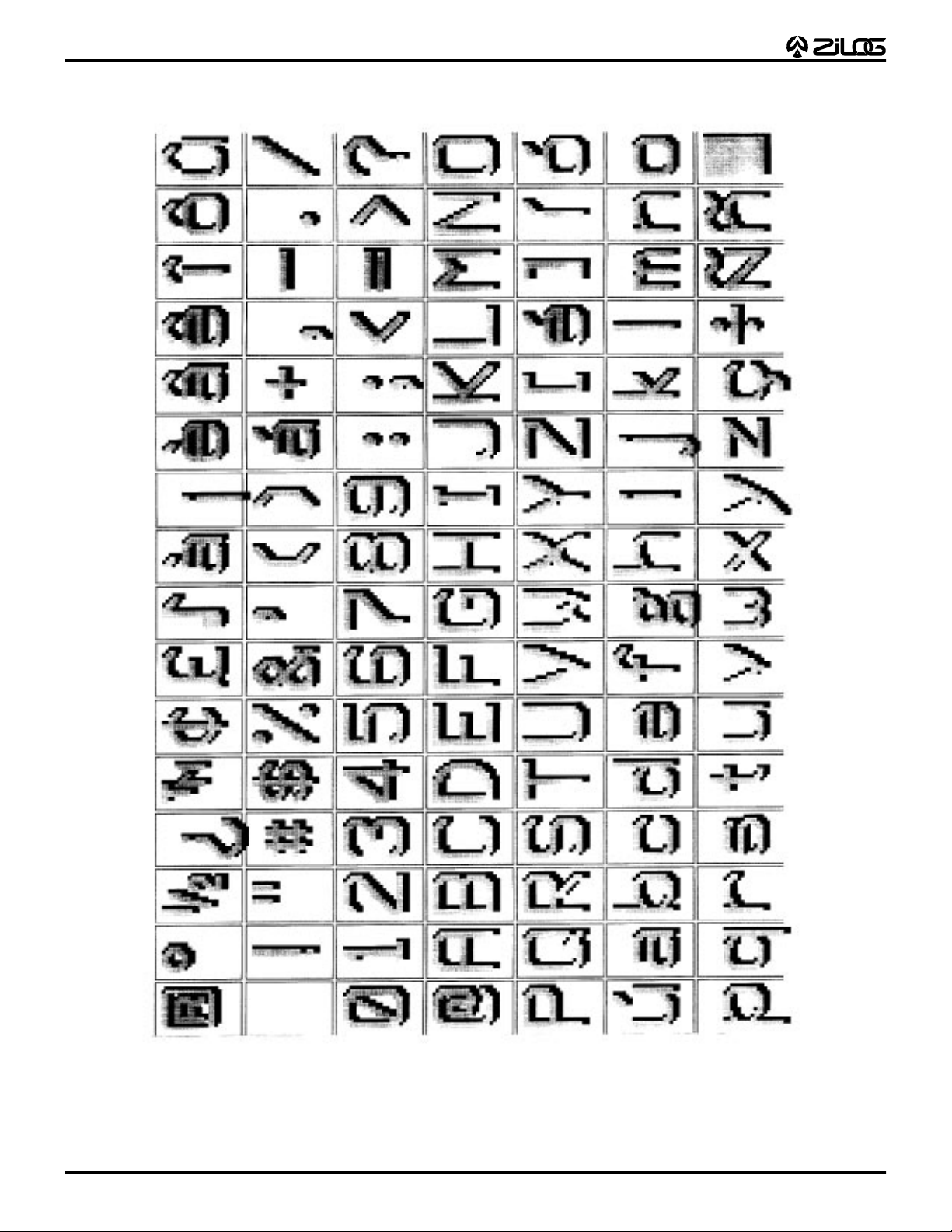
Figure 4. Z86129 Standard Character Map and Font
DS96TEL0200 11
Z86129/130/131
NTSC Line 21 Decoder P R E L I M I N A R Y
Z86129/130/131 FUNCTIONAL DESCRIPTION (Continued)
Figure 5. Caption Display Mode, Drop Shadow
12 DS96TEL0200
Z86129/130/131
1
P R E L I M I N A R Y NTSC Line 21 Decoder
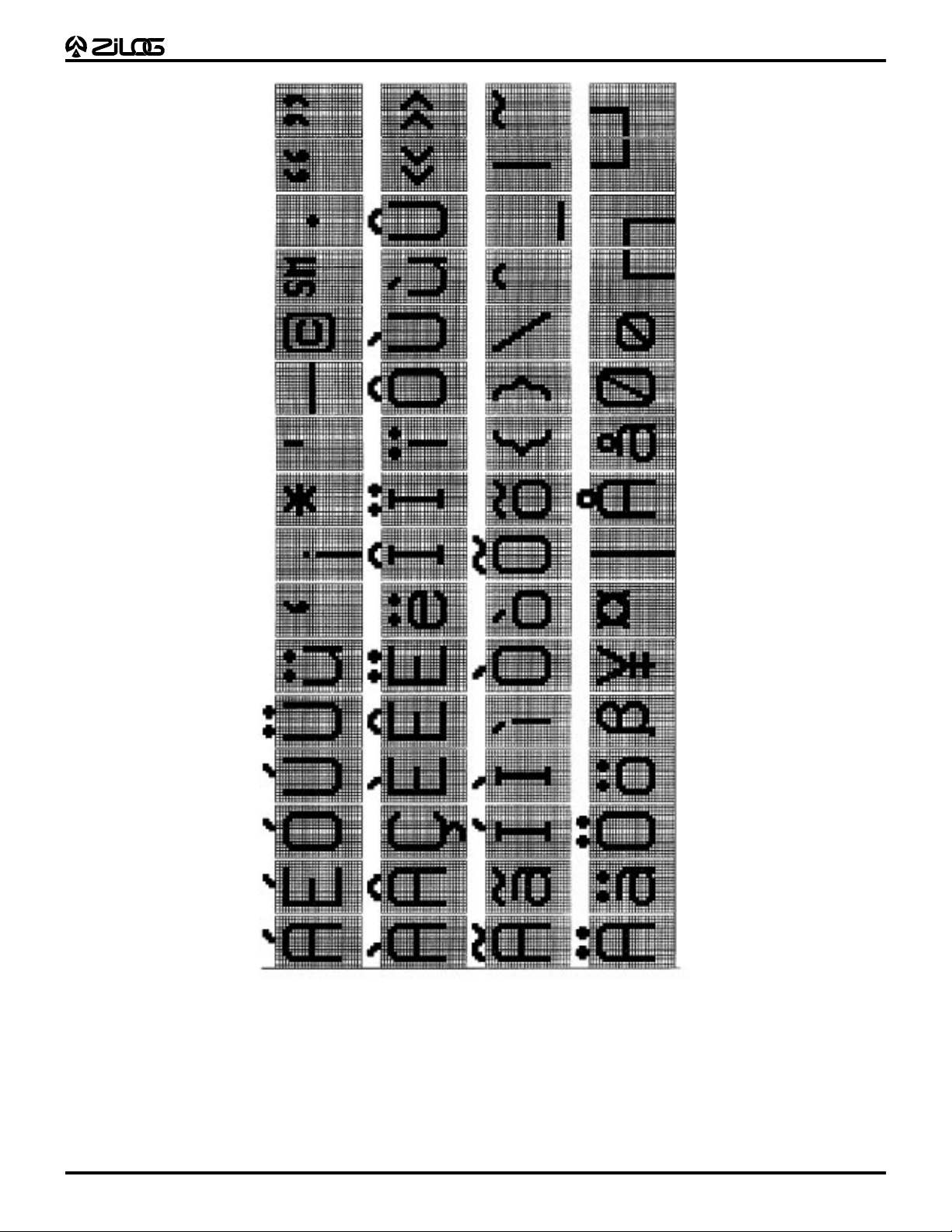
Figure 6. Extended Characters Font
DS96TEL0200 13

Z86129/130/131
NTSC Line 21 Decoder P R E L I M I N A R Y
Z86129/130/131 FUNCTIONAL DESCRIPTION (Continued)
Text Mode Display (Z86129 only)
When TEXT mode is selected, a black box will be
displayed as long as valid Line 21 code in the field selected
is being detected. The Z86129 provides the option to make
the box blue instead of black. This option holds for
Captions as well as Text.
The default TEXT display mode uses a 15 row by 34
character black box. TEXT characters will be displayed as
they are received starting in the top row. Successive
carriage returns will move the display down successive
rows until all 15 rows have been displayed. Thereafter, the
text will scroll up as new characters are added to the
bottom row.
If the data for the selected channel is interrupted by a
command for another channel, data processing will stop
but the display will remain. When a Resume Text
command is received, data processing will resume and the
new characters will be added starting at the position that
the display row/column pointer was in at the interruption of
data processing. If a Start Text command is received, the
display will be cleared and new characters will be
displayed starting in row 1, column 1 (left side).
The number of display rows and the location (base row) of
the TEXT box, can be altered by the user. In this way, the
user can decide how much of the screen can be covered
when displaying non-program related information.
When scrolling, the display will shift one scan line per
frame until a complete row has been scrolled. If a carriage
return is received before scrolling is complete, the display
will immediately complete the “scroll” by jumping up the
remaining scan lines and start displaying the new text.
Caption Mode Display (Z86129 only)
According to the FCC specifications Caption data can
appear in any of the 15 display rows but a single caption
may consist of no more than 4 rows. The form of the
caption display depends on the caption mode indicated by
the transmitted caption command, Pop-on, Paint-on or
Roll-up. The Z86129 can display a single caption having
as many as eight rows. When any of the CAPTION display
modes have been selected, the screen will be transparent.
(Display box is only present when a caption is being
displayed.)
Pop-on captions work with two caption memories. One of
them is normally displayed while the other is being used to
accumulate new caption data. A new caption is popped-on
by swapping the two memories with the End Of Caption
(EOC) command. When the on-screen memory is erased,
the screen is blank (transparent) and the memory will
default to the row/column pointer at row 1, column 1 and
monochrome non-underlined.
When caption mode is selected, the decoder will process
any data following the Resume Caption Loading (RCL)
command (or the EOC). Normally, this command will be
followed by a Preamble Address Code (PAC) to indicate
the row, column and character attributes to be used with
the following data. If no PAC is received the data will be
added to the location last indicated by the row/column
pointer prior to the receipt of the RCL command.
Paint-on caption mode is essentially equivalent to the Popon mode except that the data received after the Resume
Direct Captioning (RDC) command is written to the onscreen memory rather than the off-screen memory. All the
rules for PACs, Midcodes, and so on, are otherwise the
same.
Roll-up caption mode presents a “text” like display that is
limited to 2, 3 or 4 rows, depending on the Resume Rollup (RUn) command used. The PAC following the RUn
command is used as the BASE ROW for the ROLL-UP
display. The BASE ROW will be the “bottom” row of the
ROLL-UP display. In this case, the black box does not
appear until characters are being displayed and the box is
only wide enough to provide a leading and trailing box in
each line. The new data appears in the bottom row and as
each carriage return is received, the row scrolls up and the
new data added to the bottom. When the number of rows
indicated by the Resume command has been reached, the
data in the top row scrolls off as new data is added to the
bottom.
The TAB (INDENT) PAC permits placing Captions starting
at 4 character boundaries in any caption row. The TAB
OFFSET command provides the means for adjusting the
starting position for a Caption at any column position in the
current row.
14 DS96TEL0200
Z86129/130/131
1
P R E L I M I N A R Y NTSC Line 21 Decoder
XDS Display Modes (Z86129 only)
Two preprogrammed XDS display modes are provided.
One provides information about the current program that
would be of interest for “channel grazing”. The second
display shows the grazing packets plus additional XDS
packets which will inform the viewer about the program
content. Information will be displayed as it is received. The
displays use drop shadow mode with 15 scan lines per
row.
The XDSG mode is the GRAZE (channel grazing) display
(Figure 7). The display will contain three rows of
information at the top of the screen, formatted for easy
reading. They will contain the following XDS packet
information:
OSD Row 1 Network Name, Call Letters (Green)
OSD Row 2 Program Name (Italics, Underline, White)
OSD Row 3 Program Length, Time In Show (Cyan)
OSD Row 1
Network Name
Program Name
Program Length
OSD Row 2
Call Letters
Time in Show
Since 15 scan lines per row mode is being used, rows 1013 will appear at the bottom of the screen.
OSD Row 1 Network Name, Call Letters (Green)
OSD Row 2 Program Name (Italics, Underline,
White)
OSD Row 3 Program Length, Program Type, Time In
Show (Cyan)
OSD Row 10 Program Description Row 1 (Yellow)
OSD Row 11 Program Description Row 2 (Yellow)
OSD Row 12 Program Description Row 3 (Yellow)
OSD Row 13 Program Description Row 4 (Yellow)
OSD Row 1
Network Name
Program Name
Program Length
OSD Row 3
Program Description information goes
here on OSD rows 10, 11
OSD Row 2
Call Letters
Time in Show
12 and,
13
OSD Row 3
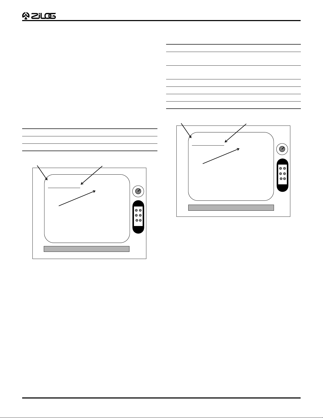
Figure 7. XDSG (Graze) Mode Sample Display
The XDSF mode is the FULL (information) display (Figure
8). This display shows the same information as the
GRAZE display and adds the program type as well the first
four program description rows (if transmitted). Although
XDS defines eight program description rows, the first four
are identified as containing the most important information.
The display of Program Description is limited to the first
four rows because eight rows would obscure much of the
screen and because more than four rows is not likely to be
sent due to the time required for transmission.
Figure 8. XDSF Mode Sample Display
When an XDS display mode has been selected, the
information will be displayed as the appropriate packets
are received. The display will remain on screen as long as
valid XDS data continues to be received. If the 16 Second
Erase Timer is enabled (the default condition), the XDS
display will be erased when no valid XDS data has been
received for 16 Seconds. If subsequent XDS data is
received with displayable packets, that information will
reappear on the screen. XDS data recovery can be active
in the XDS display mode.
The XDS display mode is turned off by selecting a different
display mode.
DS96TEL0200 15

Z86129/130/131
NTSC Line 21 Decoder P R E L I M I N A R Y
Display Erase and Autoblanking
(Z86129 only)
The display is erased in the TEXT mode by the Start Text
command (but the box is maintained) and in the CAPTION
mode by the Erase Displayed Memory (EDM) command.
The non-displayed memory can be erased by the Erase
Non-displayed Memory (ENM) command.
Four other events can also cause the display to be erased.
1. A change in the display mode, such as from CC1 to
T1, CC1 to XDSF, and so forth, will clear the memory
and hence the display.
2. A loss of video lock, such as on a channel change, will
cause the screen to be cleared. The current active
display mode will not be changed. For example if CC1
was selected and ON before the channel change the
device will remain in the CC1/ON state after channel
change.
3. The third action that will clear the displayed memory is
when the autoblanking circuit is activated. The
autoblanking circuit monitors the presence of a Line 21
waveform in the video field corresponding to the data
channel selected for display. The decoder is held in
the Decoder OFF (TV) state until a Line 21 waveform
is continuously detected for a period of 0.5 seconds.
Once a valid Line 21 waveform has been detected for
0.5 seconds, and assuming that the user has selected
the Decoder ON state, the normal display for the data
channel selected will be presented. The autoblanking
circuit will be not activate again until a valid Line 21
waveform has been lost for 1.5 seconds. Any data
received during the 1.5 second period will reset the
counter so that autoblanking will only be activated on
continuous loss of the Line 21 waveform for 1.5
seconds. Note: Valid Line 21 waveform is defined as
the presence of a 7-cycle run-in clock and a start bit on
Line 21 of the field being examined.
4. The fourth method of clearing the screen is by the
action of the 16 Second Erase Timer.
This function is
only active when a CAPTION or XDS display mode
has been selected.
If no data is received for the
display channel selected for a 16 second period, the
on-screen memory will be erased. The decoder will
still be in the selected channel and with the decoder
ON, so that when data for the selected channels
resumes, it will be displayed.
Z86129/130/131 FEATURE SET
The primary features of the Z86129/130/131 are briefly
described below. More complete descriptions can be
found in later sections of this document.
VBI Data Processing
The Z86129/130/131 extracts the data in Line 21 of the
incoming video. All data channels, in both video fields are
supported. Specifically, the Z86129 can:
■ Process data from both fields of Line 21
simultaneously.
■ Output XDS data through the serial port while
displaying selected data.
■ Output XDS data through the serial port raw or filtered.
■ XDS filters are selectable from a list of pre-
programmed values including Program Rating and
Time of Day/Local Time.
■ NTSC or PAL operation selectable.
The data extracted from Line 21 of the incoming video by
the Z86129 may be displayed in different ways according
to the user selection and the type of data. The display
features available on the Z86129 only are:
■ Ten different Line 21 data display modes; CC1-CC4,
T1-T4, plus two standard templates for XDS displays.
■ Pop-on, Paint-on and Roll-up CAPTION displays.
■ TEXT display default is a full screen, 15 row display.
■ User can vertically reduce and reposition the TEXT
display as desired.
■ Color or Monochrome display mode selectable.
■ XDSG Display Mode (channel grazing): automatic
display of Network Name, Call Letters, Program
Name, Program Length, and Time In Show data
packets.
■ XDSF Display Mode (full information): automatic
display of XDSG Display Mode information plus:
Program Type (only basic types), and Program
Description.
16 DS96TEL0200

Z86129/130/131
1
P R E L I M I N A R Y NTSC Line 21 Decoder
General Purpose OSD Modes (Z86129 only)
In addition to displaying data extracted from Line 21 of the
incoming video, the Z86129 can display information
supplied through its serial port. This is referred to as OnScreen Display (OSD) display mode. This mode provides:
■ Programmable Full Screen OSD: 15 display rows by
32 character columns
■ Graphics characters
■ Double high and double wide characters
■ Fully programmable display positioning; information
may be placed anywhere on the screen.
■ Accepts externally supplied, or internally generated
VSYNC to enable OSD even when no video is
present.
Character Set
The Z86129 has a new character set with extended
features, such as:
■ New font with descenders on lower case letters
■ Optional display mode using drop shadow font (in
other words, fringing appears on each character rather
than a solid, “black box” background).
■ EIA-608 Extended Characters
■ EIA-608 Background and Foreground attributes
■ Special framing and graphics characters for OSD
display.
■ Double High and Double Wide character display for
OSD.
Serial Communications Interface
Communications and control of the Z86129/130/131 is
through a serial control interface. Two Serial Control
Modes are available with the Z86129/130/131 performing
as a slave device. These modes are:
1. A two wire, I2C interface.
2. A three wire, serial peripheral interface (SPI).
3. A total of five device pins are dedicated to the serial
control port function. These pins are designated as:
Table 2. Z86129/130/131 Serial Control Signals
Signal SMS SCK SDA SDO SEN
Pin # 615 14 16 4
I/O I I I/O O I
I2C
0 CLK Data NA 1
SPI 1 CLK Data In Data Out Enable
Notes:
SMS = Serial Mode Select High = SPI and Low = I
SCK = Serial port clock for either Serial Mode.
SDA = Serial port data for I
SDO = Serial Data Out for SPI Mode. Not used in I
SEN = SPI Mode Enable signal. Must be High for I
2
C Mode. The I2C port on the Z86129/130/131 always
I
2
C Mode and Data In for SPI Mode.
2
C
2
C Mode.
2
C Mode.
acts as a slave device. I2C Mode is selected by bringing
the SMS pin Low and the SEN pin High. SEN must remain
High whenever I2C mode is desired. If the SEN pin is
brought Low, with SMS also Low, the part will be reset.
SDA and SCK are the data and clock lines of the I2C port,
respectively. During I2C mode operation the VIN/INTRO
signal (pin 13), can be configured to generate interrupt
requests to the master device on selected events. (See
Note paragraph below.)
■ Fifteen scan lines per character row for OSD and
TEXT.
SPI Mode. SSPI Mode is selected by making the SMS pin
High. In SPI mode the Z86129/130/131 acts as a slave
device. All communications are clocked in and out as 8-bit
Note: Contact the nearest Zilog Sales office for additional
information on how to define your own custom OSD
character set.
bytes. SCK is the serial clock (input), SDA is Data-In and
SDO is Data-Out. The SEN pin enables communication
when High, when Low High High High, the SDO pin is tristate.
DS96TEL0200 17

Z86129/130/131
NTSC Line 21 Decoder P R E L I M I N A R Y
Z86129/130/131 FEATURE SET (Continued)
When SEN is brought High the part will be synchronized
and waiting for a Command. If SEN is tied High, the part
can also be synchronized by a command string. During
SPI mode operation the VIN/INTRO signal (pin 13), can be
configured to generate interrupt requests to the master
device on selected events. (See Note paragraph below.)
CAUTION: When the SEN and SMS pins are made Low
simultaneously, the part will be reset.
Interrupt Generation. The VIN/INTRO signal (pin 13) can
be configured to provide an interrupt output on selected
events. The configuration of VIN/INTRO (pin 13) is user
programmable to be either of two states:
1. An INPUT pin for acceptance of an external VSYNC
timing signal
2. An OUTPUT pin for interrupt generation on a selected
events
Note: Configuring VIN/INTRO as an output for interrupt
generation is particularly useful when implementing the
V-Chip feature in TVs and VCRs. In this configuration, Pin
13 is used to interrupt the host processor when the XDS
Program Rating data packet is found. As a result the host
processor is not burdened with monitoring or filtering the
line 21 data stream. The Z86129/130/131 filters the Line
21 data stream for the host processor, and generates an
interrupt only when the desired packet is found.
Setup and Operational Control
The Z86129/130/131 is extremely flexible and fully
programmable through its serial communication port. The
following tables provide a
Programmable Features, User Selectable Display Modes,
and Default Conditions upon Reset.
Z86129/130/131 Programmable Features
– Decoder ON/OFF
– TV scan lines per OSD row (13 or 15)
– EIA-608 extended attributes ON/OFF
– OSD drop shadow ON/OFF
– Color/Monochrome
– OSD Horizontal start position
– Text box size (# of rows)
– Text box starting row position
– NTSC or PAL
– Vertical Lock Source: Video or External VIN
– XDS Data Output, Raw or Filtered
– H Lock Source: Video or External HIN
partial list
of User-
In addition to the programmable features just listed, the
Z86129 offers a choice of eleven display modes for user
selection.
Table 3. Z86129 Display Modes
Display
Mode Display Data
CC1 L21 Closed
Captions
CC2 L21 Closed
Captions
CC3 L21 Closed
Captions
CC4 L21 Closed
Captions
T1 L21 TEXT 2 II
T2 L21 TEXT 1 I
T3 L21 TEXT 1 II
T4 L21 TEXT 2 I
XDSF XDS 2 II
XDSG XDS 2 N/A
OSD User Defined via
Serial Port
The Z86129/130/131 is initialized on RESET to the
following default conditions:
Table 4. RESET Default Conditions
Parameter Reset Condition
Display Channel CC1
Decoder OFF
TEXT Size 15 rows
Lines/Row 13
Background BOX
EIA-608 Extended Attributes ON
Data Outputs OFF
Video Standard NTSC
Data Outputs OFF
VCO Lock Video
BOX Timing 13.5usec
Vertical Lock Video
VIN/INTRO INTRO & Disabled
Horizontal Lock Video
Color/Mono Color
OSD Display Drop Shadow 15
NTSC
Field Language
1 (odd) I
1II
2 (even) I
2 N/A
lines/row
18 DS96TEL0200

P R E L I M I N A R Y NTSC Line 21 Decoder
1
SERIAL COMMUNICATIONS INTERFACE
Z86129/130/131
Commands and data are sent to and from the Z86129
through its serial communications interface. Two Serial
Control Modes are available. One mode is a two wire I2C
bus interface. The other serial mode is a three wire,
synchronous serial peripheral interface (SPI). In both
cases the Z86129/130/131 acts as a slave device.
This port is the path for setting the configuration and
operational modes of the device. It is also the port for
outputting the recovered XDS data and for inputting the
OSD data for display.
Five pins are dedicated to the control port function and one
additional pin can be configured to provide an interrupt
output. These pins are designated as shown in Table 5.
Table 5. Z86129/130/131 Serial Control Signals
Signal SMS SCK SDA SDO SEN
Pin # 615 14 16 4
I/O I I I/O O I
I2C 0 CLK Data Hi-Z 1
SPI 1 CLK Data In Data Out Enable
Notes:
SMS = Serial Mode Select High = SPI & Low =
SCK = Serial port clock for either Serial Mode.
SDA = Serial port data for
SDO = Serial Data Out for SPI Mode. Not used in
SEN = SPI Mode Enable signal. Must be High for
I2C Mode and Data In for SPI Mode.
I2C
I2C Mode.
I2C Mode.
The Z86129/130/131 can receive or transmit data under
control of the master device. The Z86129/130/131 is a
slave device. Communication is initiated when the master
device sends the start condition followed by the
Z86129/130/131 Slave Address Read byte (29h) or Slave
Address Write byte (28h). The Z86129/130/131 will
respond with an Acknowledge. The I
Least Significant Bit (LSB) of the I2C addresses listed
below in Table 6.
Table 6. Z86129/130/131 I2C Slave Addresses
READ WRITE
I2C Address
Note: When the SMS and SEN pins are both Low, the part will
be in the RESET state. Therefore the SEN pin can be used to
reset the part while in the I
to an NRESET signal or tied High if no reset is desired.
29h 28h
2
C mode. The SEN pin may be tied
2
C RD/nWR bit is the
The I2C Bus Protocol
1. Data transfer can only be started when the bus is not
busy.
2. During data transfer, data transitions must not occur
while the clock is High.
Bus Conditions are Defined as:
Not Busy: Data and Clock lines both High.
When the Vertical Lock = VIDEO, the VIN/INTRO (pin13)
is configured as an output, providing the INTRO signal.
This interrupt operation is available in either serial control
mode.
The Z86129/130/131 is able to interrupt on the occurrence
of any of several events. The master device will clear the
interrupt by writing to the Interrupt Request Register.
I2C Bus Operation
The serial control mode in use is selected by the state of
the SMS pin. When SMS is set Low, the Z86129/130/131
will be in the I2C mode. In this mode, the Z86129 also
supports a bidirectional two wire bus and data
transmission protocol. The bus is controlled by the master
device, which generates the serial clock (SCK), controls
the bus access and generates the Start and Stop
conditions. The SDA pin is the bidirectional Data line. In
this mode the SDO output is not used and the pin will be in
its high impedance state.
Start: A High to Low transition of SDA line while SCK line
is High.
Stop: A Low to High transition of SDA line while SCK line
is High.
Acknowledge: When addressed, the receiving device
must output an acknowledge after the reception of each
byte. The master device must generate the clock for the
acknowledge bit. Acknowledge is SDA=Low. Not
Acknowledge (NACK) is SDA=High.
Data: The data (SDA) is output by the transmitting device
on the falling edge of SCK, MSB first. The receiving device
will read the data, MSB first, on the rising edge of SCK.
Communication with the Z86129/130/131 is initiated when
the master device sends the Z86129/130/131 slave
address following a start condition. The Z86129/130/131
has a preset, single, seven-bit slave address. The Z86129
will respond with an acknowledge. The eighth bit of the
slave address is driven High for Read operations and Low
for Write operations.
DS96TEL0200 19

Z86129/130/131
NTSC Line 21 Decoder P R E L I M I N A R Y
SERIAL COMMUNICATIONS INTERFACE (Continued)
Writing to the I2C Bus
All write commands are either one or two byte commands.
The Z86129/130/131 is enabled when a Start condition
followed by its Slave Address Write byte is received. It will
be disabled once it deems the command to have been
completed or by a Stop condition. A new Start condition
without a Stop condition will begin a new sequence.
Therefore, successive commands may be executed by
successive strings of “Start-Slave Address-Command”
sequences without any intervening Stop condition being
sent.
Notes:
The number of data bytes to be received by the
Z86129/130/131 is inherent in the command and the
Z86129/130/131 will respond with the acknowledge signal
only for the number of bytes expected. If the master writes
more bytes than expected, there will be no acknowledge
for the extra bytes.
A write to the Z86129/130/131 should always be preceded
by executing a Status read to verify that the
Z86129/130/131 is not busy. The Status register data is
output immediately following the reception of the Slave
Address Read. If the RDY bit is set, the master device can
initiate its write sequence, always beginning with the Start
condition. The first byte of a two byte command is always
written first.
An example of the master's sequence for writing a two byte
command (after RDY had been checked) would be:
Start-Slave Address Write/Slave ACK-CMD (master)/
Slave ACK-DATA (master)/Slave ACK-Stop.
I2C-Two Byte Write (Command & Data)
STRT
SLAVE
ADDR
(WRITE=28h)
I2C-One Byte Write (Command)
WRITE
CMD
WRITE
DATA
STOP
Reading Data Using the I2C Bus
With the exception of the Serial Status (SS) register, which
may be read at any time, each read operation must be set
up before the data can be read from the serial output
registers of the Z86129/130/131. Data is set up for a read
operation either automatically or manually. XDS data
reads are set up automatically upon recovery by setting a
valid XDS FILTER register selection. All other data read
operations must be set up manually using the READ
SELECT commands RDS1 and RDS2. These commands
load the selected data byte or pair of bytes into the serial
output register(s), set the SS register RD2 bit according to
the number of data bytes requested and set the SS
register DAV bit to indicate availability of data.
2
The Z86129/130/131 I
byte read sequences. All read sequences output the SS
register as the first output byte. If the serial status DAV bit
is set, a two or three byte read sequence can then be
initiated, beginning with a new STRT condition. If the DAV
bit is not set, the I2C master device should not attempt to
read any data bytes or the desired data can be lost from
the Z86129/130/131output registers.
The number of data bytes available is indicated by the
state of the RD2 bit of the serial status. In a typical read
operation the status byte is read and the DAV and RD2 bits
are examined. If one or two data bytes are available they
are read in sequence separated by acknowledges.
Note:
In all I2C Read operations (one, two, and three byte as
defined in Figure 10) the last byte read from the
Z86129/130/131 should be acknowledged by the master
with a NACK (Not ACKnowledge). It is also necessary to
read all available data in a read operation to clear the DAV
bit and permit subsequent reads. DAV is cleared by the
master clocking out the eighth bit of the last data-byte
read. DAV is never cleared by just reading the SSB (onebyte read) alone. All data is output MSB first.
C Bus supports one, two and three
STRT
Note: Status Register RDY bit must be read and checked prior to the
STRT condition of either WRITE sequence above. See One Byte
Read (Status Only) in Figure 10 for more information on reading the
Status Register.
Figure 9. I
SLAVE
ADDR
(WRITE=28h)
2
C Bus WRITE (Command)
WRITE
CMD
STOP
20 DS96TEL0200

Z86129/130/131
1
O
P R E L I M I N A R Y NTSC Line 21 Decoder
The master's sequence for reading two
data bytes
(total
of three bytes including SSB) from the Z86129/130/131 is
given as:
Start-Slave Address Read/Slave ACK-SS Byte/Master
ACK-Byte (slave)/Master ACK-Byte (slave)/Master NACKStop
I2C-One Byte Write (Status Only)
STRT
SLAVE
ADDR
(READ=29h)
SERIAL
STATUS
(SSB)
STOP
NACK
I2C-Two Byte Read (Status & Data1)
STRT
SLAVE
ADDR
(READ=29h)
SERIAL
STATUS
(SSB)
READ
DATA1
STOP
NACK
I2C-Three Byte Read (Status, Data1, & Data2)
NACK
READ
DATA2
STOP
STRT
Note: In all I2C Read operations defined herein, the last byte read
from the Z86129/130/131 must be acknowledged by the master
with a NACK (Not ACKnowledge).
SLAVE
ADDR
(READ=29h)
Figure 10. I
SERIAL
STATUS
(SSB)
2
C Bus READ (Command)
READ
DATA1
Clock and Data Transitions. The SCK and SDA bus lines
are normally pulled High with a resistor. Data on the SDA
bus may only change during SCK Low time periods. Data
changes during SCK High periods will indicate a start or
stop condition as defined in Table 7.
Start Condition. A High-to-Low transition of SDA with
SCK High is a start condition which must precede any
other command.
Stop Condition. A Low-to-High transition of SDA with
SCK High is a stop condition which terminates all
communications.
Acknowledge. All address and data words are serially
transmitted to and from the Z86129/130/131 in eight bit
words. A ninth bit time is used for the acknowledge. The
acknowledging device does so by pulling the SDA bus Low
during the ninth bit. A Not Acknowledge (NACK) is given
by SDA=High during the ninth clock time.
t
R
t
SU.ST
t
BUF
SCK
t
SU.STA
t
HD.STA
SDA (IN)
SDA (OUT)
t
t
F
t
t
AA
High
HD.DAT
t
Low
t
SU.DAT
t
DH
Figure 11. I2C Serial Timing
Table 7. I2C Serial Timing Min/max
Symbol Parameter Min Max Units
f
SCK
t
LOW
t
High
t
R
t
F
t
AA
t
BUF
t
HD.STA
t
SU.STA
t
HD.DAT
t
SU.DAT
t
SU.STO
t
DH
t
I
Clock Frequency 100 kHz
Clock Pulse Width Low 4.7 – µs
Clock Pulse Width High 4.0 – µs
SDA and SCL Rise Time – 1.0 µs
SDA and SCL Fall Time – 300 ns
Clock Low to Data Out Valid 0.1 3.5 µs
Bus Free Time 4.7 – µs
Start Hold Time 4.0 – µs
Start Set-up Time 4.7 – µs
Data In Hold Time 0 – µs
Data In Set-up Time 250 – ns
Stop Set-up Time 4.7 – µs
Data Out Hold Time 100 – ns
Input Filter Time Constant 100 ns
DS96TEL0200 21

Z86129/130/131
NTSC Line 21 Decoder P R E L I M I N A R Y
SERIAL COMMUNICATIONS INTERFACE (Continued)
SPI Bus Operation
When the SMS pin is High the Z86129/130/131 will be in
the SPI serial control mode. The clock line should be tied
to the SCK pin. The DATA IN signal and DATA OUT signal
from the master device should be connected to the SDA
and SDO pins respectively. The SEN pin is used to select
the Z86129/130/131 when there are multiple peripherals
on the bus.
As noted above, when both the SMS and SEN pins are
Low, the part is in the RESET state. When the SPI bus is
used in a dedicated fashion between the master and the
Z86129/130/131, both the SEN and SMS pins would be
tied High. The RESET function would require that both of
these pins be tied to the NRESET signal. To ensure
synchronization, the master should send the serial
synchronization signal after the reset is released.
When the SPI mode is used in a multiple peripheral
environment, the SEN pin is used as the Z86129/130/131
enable signal. SMS could then be used for the NRESET
signal as long as reset was only applied while SEN was
Low. In this case, there would be no need for the master to
send a serial synchronization string after reset if there was
at least 100 ns between the end of reset and the start of
port enable.
A command string can be interrupted at any time and the
port resynchronized by sending the Serial Sync signal or
by the rising edge of SEN.
The SPI bus is a three wire bus when used in a dedicated
manner between the Z86129/130/131 and the master
device. If other peripherals are connected to the bus, then
the SEN pin must be used to place this device on the bus
at the appropriate time. When SEN is Low, the SDO pin
will be tri-state and transitions on the SCK and SDA pins
will be ignored.
If data output is not required from the Z86129/130/131,
then control can be accomplished using only the SCK and
SDA pins. Since this type of operation precludes the ability
to check the RDY bit, it is very important that commands
be spaced by at least two frames (133 µsec) to ensure that
one command has been executed before initiating
another.
The bus is controlled by the master device, which
generates the serial clock (SCK) and initiates all actions.
Clocking data in on SDA will simultaneously produce data
out on SDO. The master should always check for the
appropriate handshake signal before executing any
command other than NOP.
Writing to the part requires that the RDY bit be set while
reading from the part requires checking the SS register to
see if the DAV bit is set. Both of these bits are contained in
the Serial Status (SS) register. Writing to the
Z86129/130/131 will concurrently output the contents of
the SS register, MSB first, unless other data is being
output as a result of one of the READ commands. If it is
desired to read the SS without executing a command, the
NOP command can be written at any time, even if the
serial status RDY bit is not set.
The RDY status bit is driven onto the SDO pin between
command transmissions. The controlling MCU can test the
state of this pin without clocking in order to determine if
subsequent serial transfers are possible. The DAV bit can
only be checked by outputting the contents of the SS
register.
Writing to the SPI Bus
All write commands are either one or two byte commands.
The number of data bytes to be received by the
Z86129/130/131 is inherent in the command. If the master
writes more bytes than expected, the command may be
overwritten or corrupted by the extraneous bytes.
A write to the Z86129/130/131 should always be preceded
by executing a Status read to verify that the device is
ready. The serial status is output by the device concurrent
with the input of any command byte. If the RDY bit of the
serial status register is set, the master device can write a
new command.
The command and data bytes are written MSB first. The
first byte of a two byte command is sent first. The bits are
clocked into the Z86129/130/131 by placing the data on
the SDA input and bringing SCK High.
Reading Data Using the SPI Bus
With the exception of the SS read, each read operation
must be set up before the data can actually be read from
the serial output registers of the device. Data is set up for
a read operation either automatically or manually. XDS
data is set up for READ automatically upon recovery by
setting a valid XDS FILTER register selection. All other
data read operations must be set up manually, using the
READ SELECT commands RDS1 and RDS2. These
commands load the selected data byte or pair of bytes into
the serial output registers, set the SS register RD2 bit
according to the number of data bytes requested and set
the serial status DAV bit to indicate availability of data.
The Z86129/130/131 SPI Bus supports two and three byte
read sequences. In SPI mode, the SS must be read before
a read sequence is started so that the DAV and RD2 bits
can be checked. The number of data bytes available is
indicated by the state of the RD2 bit. The special command
READ1 or READ2 is then used to read the one or two
available data bytes. The serial status is clocked out during
22 DS96TEL0200

Z86129/130/131
1
P R E L I M I N A R Y NTSC Line 21 Decoder
the write of the READ1 or READ2 command. The data
byte or bytes are then clocked-out in sequence, MSB first,
while NOP commands are written into the device. Data bits
are clocked-out on the rising edge of SCK. All available
data bytes must be read to clear the DAV bit and permit
subsequent reads.
The SPI Bus Protocol
1. The first bit of the first output byte is driven out on SDO
following the rising edge of SCK on the last bit (LSB)
of the READ1 or READ2 command.
2. Three-wire bus with Clock signal on SCK pin, Serial
Data Input on SDA pin and Serial Data Output on SDO
pin.
COMMANDS
Serial Port Commands
The majority of the Z86129/130/131 commands are
common to both the I2C and SPI modes. In the I2C mode,
the commands must be contained within the Start-Slave
Address-etc. sequence.
Note: In the following Command descriptions, the letter 'h'
following a command code designates Hexadecimal
notation.
3. SEN pin Low disabled the port, placing SDO in tristate. Signal transitions on SCK and SDA are ignored.
4. SEN pin High enables the port for operation.
5. SEN and SMS pins Low is a hardware reset for the
part. These pins must be held Low for at least 100 ns.
6. Serial synchronization can be established by clocking
in the minimum required SSR string of FFh, FFh, FEh.
More than two bytes of FFh may be input but the string
must end with FEh.
SSB byte of FEh. At the end of the FEh byte the port is
ready for use.
Table 8. Basic Serial Commands
Serial Command Command Code Notes
RESET FBh, FCh, 00h
NOP 00h
SPI or I2C
SPI or I2C
SSB FFh,...FFh,FEh SPI mode only
Reset
RESET = FBh, FCh, 00h. RESET is a three byte
command sequence in SPI or I2C mode. The RESET
command will establish all the specified default settings in
the device, but it will not reset the serial port itself. This
sequence can be entered without RDY being set.
No Operation
NOP = 00h. NOP is a one-byte command for use in SPI or
I2C mode. The NOP command does not affect the status
of the RDY bit in the Serial Status (SS) register and can be
executed independent of the RDY status.
Serial Sync Bytes
SSB = FFh,....,FFh,FEh. Serial Sync Bytes are used in
SPI mode only. This command actually consists of a string
of single-byte commands in the form FFh,....FFh,FEh. SPI
mode communications can be synchronized by sending a
synchronizing data string to the part. This string should
consist of at least two SSB bytes of FFh followed by one
Caption/Text Display Mode Commands
CPTX = 10h-1Fh. Caption and Text display mode
commands. These commands select the desired Line 21
data stream (Closed Caption or Text) for display.
Bit
CM7
R/W R/W
0
CM6
0
CM5
0
R/W
Figure 12. CPTX-Caption/Text Display
(CPTX = 10h-1Fh)
Caption and Text display commands are one byte
commands. A data channel can be selected for display
with the display either enabled (DEC ON) or disabled
(DEC OFF). All these commands will turn off an active
XDS display mode. Table 9 summarizes the device’s
CM4
1
R/W
CM3
FLD
R/W
CM2 CM1 CM0
LANG
R/W
DONOF
CPTX
R/W R/W
DS96TEL0200 23

Z86129/130/131
NTSC Line 21 Decoder P R E L I M I N A R Y
COMMANDS (Continued)
Caption and Text display modes and the proper command
code to activate them:
Table 9. Caption and Display Commands
CPTX CPTX Command Code
Command Decoder ON Decoder OFF
CC1 17h 16h
CC2 15h 14h
CC3 1Fh 1Eh
CC4 1Dh 1Ch
T1 13h 12h
T2 11h 10h
T3 1Bh 1A
T4 19h 18
XDS Display Mode and 16 Second Erase Timer
Commands
XDS DISP = 20h-27h. XDS Display commands are one
byte commands. These commands control the selection of
XDS display modes and the state of the 16 Second Erase
Timer. The 16 Second Erase Timer is active only for
Caption and XDS display modes. The 16 Second Erase
Timer has no affect on TEXT mode displays
Table 10. XDS Display Commands
RDS1 = 40h-47h. RDS1 is a one-byte command used to
initiate a one-byte read sequence by moving the contents
of the register identified by the address field (AD00:02) of
the command to the output register. Addresses 0h-7h are
valid in the RDS1 command field AD00:02.
0
W
CM3
0
W
CM2 CM1
AD01
AD02
W
W
CM0
AD00
W
Bit
CM7
0
WW
CM6
1
CM5
0
W
CM4
Figure 13. RDS1-Read One Byte (RDS1 = 40h-47h)
RDS2 = 60h-66h. RDS2 is a one byte command which is
used to initiate a two byte read sequence by moving the
contents of the two consecutive registers, starting with the
one identified by the address portion of the command
(AD00:AD02), to the output registers and setting the RD2
bit in the SS register. Only Addresses 0h-6h are valid in the
RDS2 command field AD00:02.
Bit
7
0
WW
6
1
5
1
W
4
0
W
3
210
AD02
0
W
W
AD01
AD00
WW
XDS Display XDS Display Command Code
Command 16 Sec Tmr ON 16 Sec Tmr OFF
XDSG 23h 27h
XDSF 21h 25h
16 Second Erase
20h 24h
Timer
Note: Changing the ON/OFF state of the 16 Second Erase
Timer has no affect on the current display mode in operation.
Read And Write Commands
Read Selects. There are two Read Select commands
(RDS1 and RDS2) in the Z86129/130/131. Each
command is one byte in size and indicates that a read
should take place. RDS1 specifies that one byte will be
read from the Z86129/130/131. Likewise, RDS2 indicates
that two bytes will be read.
Figure 14. RSD2-Read Two Bytes (RDS2 = 60h-66h)
Note: For XDS data recovery, when the XDS Filter
Register (see Internal Register section) is enabled for the
desired packets, the Z86129/130/131 will automatically
establish the two byte recovery mode and move the
recovered data bytes to the output register.
24 DS96TEL0200

Z86129/130/131
1
P R E L I M I N A R Y NTSC Line 21 Decoder
Reading Data From The Z86129/130/131
READ1 = F8h:
Command to read one byte in the SPI mode.
READ2 = F9h:
Command to read two bytes in the SPI mode.
Bit
7
1
W
6
1
W
Figure 15. READx-Read x Bytes
(READ1/2 = F8h/F9h)
The READx commands do not affect the status of the RDY
bit in the Serial Status (SS) register and can be executed
independent of the RDY status.
In both serial communications modes, the DAV bit in the
SS register indicates when data is available. When the
RD2 bit is Low, DAV is cleared on the rising edge of SCK
at the LSB of the first data byte. When the RD2 bit is High,
DAV is cleared on the rising edge of SCK at the LSB of the
second data byte. The RD2 bit is only valid if DAV is High.
Reading in the I
2
C mode is selected by the R/NW bit in the
Slave Address byte. The first byte after the Slave Address
byte will be SS followed by the data in output buffers A and
5
1
W
4
1
W
21 0
3
1
0
W
W
0
RD2
WW
B in that order. If the instruction being executed is a onebyte read, then buffer A contains the read data and buffer
B contains all ones.
Writing to the Z86129/130/131
WRxx = C0h-DFh
Bit
7
1
WW
6
1
5
0
W
4
AD04
W
AD03
Figure 16. WRxx-Write Register xx
(WRx = C0h-DFh)
The WRITE commands require two bytes to execute. The
first byte is the write command and includes the Z86129
register address (AD00:04) being written. The second byte
will be the data to be written.
OSD Display Mode Commands
OSD commands are one and two byte commands. They
are used to control the loading of data for OSD display and
their presentation to the screen. Normally OSD display
mode uses 15 TV lines per display row to enhance the
screen appearance. The following tables summarize the
single- and two-byte control commands for the
Z86129/130/131 On-Screen Display.
3
AD02
W
21
AD01
WW
W
0
AD00
Table 11. Single-Byte OSD Display Mode Commands (Z86129 Only)
Command Name Code Command Function
RETURN 30h Carriage return for OSD when in TEXTSET mode
CLRE 31h OSD equivalent of delete to end of row (DER)
TEXTSET 32h Establishes a TEXT type of OSD display
POPSET 33h Establishes a pop-on type of OSD display
FLIP 36h OSD equivalent of pop-on caption end of caption (EOC)
OEDM 37h OSD equivalent of erase displayed memory
OENM 38h OSD equivalent of erase non-displayed memory
DS96TEL0200 25

Z86129/130/131
NTSC Line 21 Decoder P R E L I M I N A R Y
COMMANDS (Continued)
Table 12. Two-Byte OSD Display Mode Commands (Z86129 Only)
Command
Name
POP ROW
SEL
(with Double
High Option)
PHYS ROW
SEL
CURSOR SET A2h cch Places the cursor at the character column position designated by cc, which can be
WRITE CHAR A3h ddh Writes the data byte dd to the current cursor location and then increments the
WRITE MAP A4h rrh Maps the current physical row to the display row designated by the low nibble of
WRITE CHAR
DBL WIDE
WAIT A6h nnh Sets the RDY bit of SS and then suspends serial command execution for
Figure 17 shows the two different character sets, Graphics
or Extended, that share the address space C0h-FFh. The
Graphics Character set is in force when the OSD display
is in Drop Shadow mode (the default condition).
First
Byte
A0h rrh Sets display row and moves cursor to char column 1. The low order nibble of rr
A1h rrh Sets the physical row, where the low order nibble of rr designates the physical
A5h ddh Same as A3 command but specifies a double wide character.
Second
Byte Command Function
designates the display row. Bit 5 of rr specifies a Double High row. For example:
rr = 0Eh would select display row 14. rr = 23h would select display row three,
Double High.
row. rr can be any value from 00h to 0Fh.
any value from 00h to 20h (column 0-32). Zero is the PAC space.
cursor.
the rr byte. Bit 4 of rr = 1 enables display of the row. Bit 5 of rr = 1 indicates a
double High row.
approximately the number of frames designated by the nn byte.
The two-byte commands GRAPHICS and EXTENDED
above can be used to switch from the Graphics Characters
to the Extended Characters and vice versa. An OSD
screen can only use one set at a time.
26 DS96TEL0200

Z86129/130/131
1
P R E L I M I N A R Y NTSC Line 21 Decoder
Figure 17. Z86129 Graphics or Extended Character Set
DS96TEL0200 27

Z86129/130/131
Bit
CDRP
TENH
R/W
R/W R/W
T15
D
7
D
6
D
5
D
4
D
3
D
2
D
1
D
0
TDRP
R/W
O15
ODRP CENH
C15
R/W
R/W R/W
R/W
NTSC Line 21 Decoder P R E L I M I N A R Y
INTERNAL REGISTERS
Information controlling the setup and operation of the
Z86129/130/131 are maintained in several registers. The
user may read or alter the contents of these registers as
required.
Serial Status (SS) Register Address = Not Rqd.
Bit
D
7
RDY
RR
D
DAV
D
D
RD2
5
WOVR
6
R
4
INTR
R
D
3
ROVR
R
D
D
2
FLD
R
D
1
0
LOCK
RR
Figure 18. Serial Status Register
(Address not required)
D
-LOCK. Active High, indicating that the internal sync
0
circuits are locked. May be used as an indication of the
presence of a video signal.
-FLD. Signals the current video field. Low = Field 2,
D
1
High = Field 1.
D2-ROVR. Active High, indicating that the data available in
the output buffer has not been read out and new data has
been written over it.
D3-INTR. Active High, indicating that an interrupt other
than DAV is pending.
D4-WOVR. Active High, indicating a serial input data
overrun.
D5-RD2. Signals the number of bytes available for output.
Low = 1 byte, High = 2 bytes.
D
-MONO. Selects monochrome operation. Active High,
1
indicating that character luminance will be output on all
three color pins (RGB). The default is Low, selecting
COLOR operation.
D2-HLK. Selects the horizontal signal source to be used to
lock the VCO: Low = Internal, High = HIN. The default is
Internal.
D3-VLK. Selects the vertical signal source to be used to
establish vertical sync lock: Low = Internal, High = VIN.
The default is Internal. When Internal lock is enabled the
VIN/INTRO pin will default to the INTRO output mode.
Interrupts should not be selected in the Interrupt Mask
register if VLK mode is used.
. Reserved
D
4-D7
Display Register Address = 01h
Figure 20. Display Register (Address = 01h)
D0-TDRP. Selects Drop Shadow or Full Box in TEXT
mode: High = DROP SHADOW and Low = BOX. The
default is Low.
D1-T15. Selects the number of TV lines per character row
in a TEXT display: High = 15 lines/row and Low = 13
lines/row. The default is Low.
D6-DAV. Active High, indicating that data is available to be
read out.
D7-RDY. Active High, indicating that the port input buffer is
empty. Only the NOP, RESET and READ instructions may
be sent if RDY is Low.
Configuration Register Address = 00h.
D2-TENH. Enables Enhanced Attributes for a TEXT
display: High = Disabled, Low = Enabled. The default is
Low.
D3-CDRP. Selects Drop Shadow or Full Box in CAPTION
mode: High = DROP SHADOW and Low = BOX. The
default is Low.
D4-C15. Selects the number of TV lines per character row
Bit
D
res
7
D
res res
D
6
D
5
4
res
VLK
R/W
D
D
D
3
HLK
R/W
2
MONO
R/W R/W
D
1
0
TVS
in a CAPTION display: High = 15 lines/row and Low = 13
lines/row. The default is Low.
D5-CENH. Enables Enhanced Attributes for a CAPTION
display: High = Disabled, Low = Enabled. The default is
Low.
Figure 19. Configuration Register (Address = 00h)
Note: OSD and XDS display modes always have
-TVS. Selects the television standard. High selects PAL
D
0
Enhanced Attributes enabled.
and Low selects NTSC. The default is NTSC. When PAL
is selected the display defaults to 15 TV scan lines per
display row.
28 DS96TEL0200

Z86129/130/131
1
Bit
SCH
XDS
RR
res
res res
res
res
res
D
7
D
6
D
5
D
4
D
3
D
2
D
1
D
0
Bit
R/W
R/W R/W
D
7
D
6
D
5
D
4
D
3
D
2
D
1
D
0
R/W
R/W
R/W R/W
R/W
MISC
CHAN FUTR
CURR
s
2
s
1
s
0
PUBL
P R E L I M I N A R Y NTSC Line 21 Decoder
D6-ODRP. Selects Drop Shadow or Full Box in the OSD
and XDS display modes: High = DROP SHADOW and
Low = BOX. The default is High.
D7-O15. Selects the number of TV lines per character row
in the OSD and XDS display modes: High = 15 lines/row
and Low = 13 lines/row. The default is High.
H Position Register Address = 02h
Bit
D
7
BLUBX
R/W
D
6
HPO h
R/W
D
5
5
R/W R/W
D
D
4
h
4
R/W
D
D
3
2
h
h
3
2
R/W R/W
R/W
D
1
0
h
h
1
0
Figure 21. H Position Register (Address = 02h)
D0-D5-h0-h5. Used to set the Horizontal Timing of the
display. The default value in this register is 26h. Each
count change represents an incremental timing change of
330 ns. Decreasing the value of this field moves the
display to the RIGHT. Conversely, increasing the value of
this field moves the display to the LEFT.
Line 21 Activity Register Address = 04h
Figure 23. Line 21 Activity Register (Address = 04h)
D
-SCH. Indicates data being processed in the Data
0
Channel selected for display. Will become inactive if no
data is received for the selected channel within the
previous 16 seconds: High = Active, Low = Inactive. The
reset state is Low.
D1-XDS. Indicates XDS data is being processed. Will
become inactive if no XDS data is received within the
previous 16 seconds: High = Active, Low = Inactive. The
reset state is Low.
. Reserved.
D
2-D7
XDS Filter Register Address = 05h
-HPO. Set the polarity to be used for locking to the HIN
D
6
signal when in the EXT HLK mode: Low = Rising Edge,
High = Falling Edge. The default is Low.
D7-BLUBX. Designates color of BOX: High = Blue Box and
Low = Black Box. The default is Low.
Text Position Register Address = 03h
Bit
D
y
R/W
7
3
R/W
D
D
6
y
2
R/W
D
5
y
1
R/W
D
D
D
3
4
y
x
0
R/W
2
x
3
2
R/W R/W
R/W
D
1
0
x
x
1
0
Figure 22. Text Position Register (Address = 03h)
D
0-D3-x0-x3
. Sets the Number Of Rows in the TEXT
display. The default is 15 rows.
D4-D7-y0-y3. Sets the Base Row of the TEXT display.
The default value in this register is set to FFh, which
produces a 15-row display with base row 15. Entering a
new value in this register can alter the size and placement
of the TEXT display. For example, to produce an 8 row
TEXT display with a base row of 12, this register should be
set to C8h. If the value of the x and y bits result in a display
where TEXT rows are off the top of the screen, then the
first row of the TEXT display will start in row 1 and have the
number of rows determined by the x value.
Figure 24. XDS Filter Register (Address = 05h)
-CURR. Selects Current Class packets for output
D
0
through the Serial Control port when XDS recovery has
been enabled.
D1-FUTR. Selects Future Class packets for output through
the Serial Control port when XDS recovery has been
enabled.
D2-CHAN. Selects Channel Information Class packets for
output through the Serial Control port when XDS recovery
has been enabled.
D3-MISC. Selects Miscellaneous Class packets for output
through the Serial Control port when XDS recovery has
been enabled.
D4-PUBL. Selects Public Service Class packets for output
through the Serial Control port when XDS recovery has
been enabled.
DS96TEL0200 29

Z86129/130/131
Bit
R/W
R/W R/W
D
7
D
6
D
5
D
4
D
3
D
2
D
1
D
0
R/W
R/W
R/W R/W
R/W
dLOK
EOF DLE
DAV
dTXT
dCAP dXDS
dSCH
NTSC Line 21 Decoder P R E L I M I N A R Y
INTERNAL REGISTERS (Continued)
D5-D7-s0-s2. Selects a set of secondary parameters,
tabulated below, to be used in filtering the XDS data when
XDS recovery has been enabled.
Table 13. XDS Secondary Filter Settings
Secondary Filter Filter Value (s0:s2)
All 0h
Time Information 1h
In Band Only 2h
Program Rating (Note #4) 3h
VCR Information 4h
Reserved 5h
Reserved 6h
Reserved 7h
Notes:
1. Setting this register to 00h turns XDS data recovery off.
Setting bits D
the Classes selected as qualified by the Secondary Filter
(bits D
5-D7
data will be output (even Reserved and Undefined).
2. The Time Information Only selection includes the Time of
Day (TOD) and Local Time Zone (LTZ) packets.
3. VCR Information will select TOD, LTZ, Net ID, Local Call
Letters, Impulse Capture, Tape Delay, Composite 2 and
Out of Band Channel Number packets for recovery.
4. Program rating filter available on Z86129 and Z86130
only.
through D4 enables XDS data recovery for
0
). If Bits D0-D4 are all set to 1, all Classes of XDS
-dLOK. Active High, indicating that the state of the
D
3
LOCK signal has changed. The SS register must be read
to determine the current state.
D4-dSCH. Active High, indicating that a change in selected
channel activity has occurred. The Line 21 Activity register
must be read in order to determine if the selected data
channel is active.
D5-dXDS. Active High, indicating that a change in XDS
activity has occurred. The Line 21 Activity register must be
read to determine if XDS data is active.
D6-dCAP. Active High, indicating that a change in a
caption data channel activity has occurred. The Caption
Activity Register (Address 08h) must be read to determine
exactly which caption channels are now active.
-dTXT. Active High, indicating that a change in a TEXT
D
7
data channel activity has occurred. The Caption Activity
Register (Address 08h) must be read to determine exactly
which TEXT channels are now active.
Note: Except as noted for the case of D1 and D2 above,
the master device must write a 1 to the appropriate bit in
the Interrupt Request Register to clear the Interrupt.
Writing a 1 to any valid bit position the Interrupt Request
Register is equivalent to CLEARing a interrupt request on
that bit.
Interrupt Mask Register Address = 07h
Interrupt Request Register Address = 06h
Bit
D
dTXT
R/W
7
dCAP
R/W
D
6
D
dXDS
R/W R/W
D
5
dSCH
D
D
D
3
4
dLOK
R/W
2
EOF DLE
R
D
1
0
res
R
R
Figure 25. Interrupt Request Register (Address = 06h)
D
-res. Reserved.
0
D1-DLE. Active High, indicating that the data line has
ended. This bit will clear in each field a few lines after row
15.
D2-EOF. Active High, indicating that the video signal is
currently at the end of a field. This bit will clear in each field
a few lines after row 15.
Figure 26. Interrupt Mask Register Address = 07h
This register identifies which activities in the Interrupt
Request Register will be used to cause an interrupt.
Setting a bit to a 1 enables the interrupt when the
corresponding event becomes active. Setting all bits of this
register to zero disables interrupts.
30 DS96TEL0200

Z86129/130/131
1
P R E L I M I N A R Y NTSC Line 21 Decoder
Caption Activity Register Address = 08h
Bit
D
7
T4
R
D
6
T3 T2
R
D
5
RR
D
T1
D
D
3
4
CC4
CC3 CC2
R
D
2
R
R
D
1
0
CC1
R
Figure 27. Caption Activity Register (Address = 08h)
D
-Activity Bits. Activity bits for Line 21 data channels
0-D7
CC1-T4. Each bit will be set High when a mode setting
command for its data channel has been received on Line
21. The bit will be cleared to the Low state if no activity is
detected in that data channel during the next 12-16
seconds or if there is a loss of lock.
XDS Data Recovery
The Z86129/130/131 is able to recover Extended Data
Services (XDS) information from the input video signal.
This data, formatted according to EIA-608, can contain a
wide variety of information about current and future
programs, the channel currently tuned, other channels and
miscellaneous data including time of day.
XDS data is only present in the even field. The
Z86129/130/131 can recover XDS data even while
performing its normal caption decoder or OSD functions.
XDS data packets are tagged according to a Class/Type
system defined by EIA-608. The Z86129/130/131 can be
programmed to filter the XDS data stream to extract only
the classes of interest to the application. An additional
level of filtering is provided that permits selection of certain
groups of packets that are of use in specific applications.
XDS filtering reduces the traffic on the serial bus, reduces
the load of the TV/VCR control processor and simplifies
external XDS decoding.
XDS data recovery is enabled by selecting one or more
classes in the XDS Filter register. Optionally, a secondary
filter code can be specified which further limits the packets
to be recovered. Once XDS recovery is enabled filtered
data pairs will be loaded into the serial output registers of
the Z86129/130/131 immediately upon receipt and in the
order received. The DAV and RD2 bits of the Serial Status
(SS) register will then go High, indicating the availability of
two output bytes. The external TV control processor does
not need to send a READ SELECT command in order to
read these data bytes.
When the XDS Filter register is set to 00h (the default
state) XDS recovery is disabled.
CAUTION: When XDS data recovery is enabled, the
external controller should never perform any other read
operation, except SS reads, in the beginning of field 2. This
is most easily accomplished by using the end of field
(EOF) or data line end (DLE) interrupt to locate the end of
field 2 or the vertical blanking interval (VBI) of field 1, and
then perform the READ SELECT and READ functions
during this portion of the video frame. Commands other
than READ SELECTS will not interfere with XDS data
recovery regardless of their position in the video frame.
Some examples of Z86129/130/131 WRITE commands
that could be used to set the XDS Filter Register are
shown below. The XDS Filter Register bit assignments are
defined in the Z86129 Internal Register section of this
specification.
Table 14. XDS Data Extraction -
Example Filter Settings
{Write CMD,
Filter Code} XDS Filter Output
{C5,41} All In Band, Current Class packets
recovered.
{C5,61} Program Rating, Current Class packets
recovered
Note: This Filter May be Used for V-CHIP
Data Packet Recovery (Z86129 and Z86130
only).
{C5,1F} All XDS packets recovered.
{C5,01} All Current Class packets recovered.
{C5,28} Time information recovered. This Filter
will extract the Time of Day (TOD) and
Local Time Zone (LTZ) packets from the
Miscellaneous Class data.
Note: This Filter May be Used to implement
Auto Clock-Setting in TVs, and VCRs
{C5,9F} VCR Information recovered. Will select
TOD, LTZ, Net ID, Local Call Letters,
Impulse Capture, Tape Delay,
Composite 2 and Out of Band Channel
Number packets for recovery.
Filtered XDS Data Format
Filtered XDS data is output from the Z86129/130/131 in
the order it is received on Line 21. In other words, think of
the Z86129/130/131 XDS filter function as creating a new,
smaller stream of XDS data packets. This new data stream
will look exactly as though the Class and Type specified in
the XDS Filter Register (05h) are the
on Line21 of field 2. The filtered data output from the
Z86129/130/131 will be in full compliance with EIA-608
specifications for XDS data streams; headers and control
codes intact. See Note paragraph below for a special
exception to this rule.
only data
encoded
DS96TEL0200 31

Z86129/130/131
NTSC Line 21 Decoder P R E L I M I N A R Y
INTERNAL REGISTERS (Continued)
XDS data and header information (including START,
CONTINUE, and END commands) are passed through the
filter for the XDS class and type specified in the XDS Filter
Register. All other Line 21 data is filtered out and will not
be output, or used to generate a data available flag (DAV)
in the Serial Status Register.
To properly read filtered XDS data from the
Z86129/130/131, the master device must first write the
XDS Filter Register (05h) with its desired XDS Class and
Type information. For example, in order to extract ONLY
the Line 21 Program Rating information, the master must
write the value 61h to the XDS Filter Register. The master
should then poll the state of the DAV bit in the SSR until
DAV = 1.
As soon as DAV=1, the master may initiate a 3-byte read
in the normal manner (XDS data bytes always arrive in
pairs, so it is safe to assume that RD2=1 when DAV=1 in
the SSB). A 3-byte read always yields two data bytes,
which in this case will be the first two bytes of the Current
Class, Program Rating Type XDS data stream
encountered on Line21 field 2. The master device must
then interpret those two bytes according to EIA-608
specifications for Current Class, Program Rating Type
data. Refer to EIA-608 for data formats.
The XDS filters on the Z86129/130/131 greatly reduce the
amount of field 2 data passed on to the master device for
further processing and interpretation. However, the master
device must still interpret the filtered data stream in
accordance with EIA-608. The filtered data stream from
the Z86129/130/131 will be in full compliance with EIA-
608. In other words, the filtered data stream will contain all
the XDS command and data packets, in standard EIA-608
format, but only for the selected XDS Class and Type(s).
Note: The Z86129/130 XDS filter for Program Rating
information behaves differently than all other Z86129/130
predefined XDS filters. This change has been made to
minimize the amount of data passed through the Program
Rating XDS filter, thereby minimizing the interpretation
and communications load on the master device. When the
XDS Filter Register is set to 61h (Class=01h (Current),
Type=05h (Program Rating) the only data from Line 21
field 2 that will pass through the filter is:
1. Program Rating Packet: [xxh,00h]. The Current Class
Program Rating data byte pair as defined in EIA-608.
The program’s rating is encoded per EIA-608 in the
byte xxh.
2. The END Packet [0Fh,CHKSUM]. A two-byte packet
that includes a CHKSUM computed per EIA-608. The
checksum calculation includes the START packet
[01h,05h] even though this value was not passed
through the filter.
32 DS96TEL0200

P R E L I M I N A R Y NTSC Line 21 Decoder
1
Z86129 COMMANDS AND REGISTER SUMMARY
Table 15. Z86129 Summary of Control Commands
Z86129/130/131
Cmd.
Name Cmd. Code Function
RESET FBh,FCh,00h
NOP 00h
SSB FFh,...Fh,FEh Serial Sync Bytes are used in SPI mode only. This command actually consists of a string
CPTX 10h-1Fh Selects a Closed Caption (CC1-CC4) or TEXT (T1-T4) data channel for processing or
DISP 20h-28h Selects a preprogrammed XDS screen template for display, with or without 16 Second
RDS1 40h-47h RDS1 is a one-byte command used to initiate a one byte read sequence by moving the
RDS2 60h-66h RDS2 is a one-byte command which is used to initiate a two-byte read sequence by
READ1 F8h Command to read one byte in the SPI mode.
READ2 F9h Command to read two bytes in the SPI mode.
WRxx C0h-DFh, XXh The WRITE commands require two bytes to execute. The first byte is the write command
RESET is a three-byte command sequence in SPI or I2C mode. The RESET command
will establish all the specified default settings in the device, but it will not reset the serial
port itself. This sequence can be entered without RDY being set.
2
NOP is a one-byte command for use in SPI or I
affect the status of the RDY bit in the Serial Status (SS) register and can be executed
independent of the RDY status.
of single-byte commands in the form FFh,....FFh,FEh. SPI mode communications can be
synchronized by sending a synchronizing data string to the part. This string should
consist of at least two SSB bytes of FFh followed by one SSB byte of FEh. At the end of
the FEh byte the port is ready for use
display
Erase timer enabled
contents of the register identified by the address field (AD00:02) of the command to the
output register. Addresses 0h-7h are valid in the RDS1 command field AD00:02.
moving the contents of the two consecutive registers, starting with the one identified by
the address portion of the command (AD00:AD02), to the output registers and setting the
RD2 bit in the SS register. Only Addresses 0h-6h are valid in the RDS2 command field
AD00:02.
and includes the Z86129 register address (AD00:04) being written. The second byte (XXh)
will be the data to be written.
C mode. The NOP command does not
DS96TEL0200 33

Z86129/130/131
NTSC Line 21 Decoder P R E L I M I N A R Y
Z86129 COMMANDS AND REGISTER SUMMARY (Continued)
Table 16. Z86129 OSD Display Mode Commands
Cmd. Name Cmd. Code Function
RETURN 30h Carriage return for OSD when in TEXTSET mode
CLRE 31h OSD equivalent of delete to end of row (DER)
TEXTSET 32h Establishes a TEXT type of OSD display
POPSET 33h Establishes a pop-on type of OSD display
FLIP 36h OSD equivalent of pop-on caption end of caption (EOC)
OEDM 37h OSD equivalent of erase displayed memory
OENM 38h OSD equivalent of erase non-displayed memory
POP ROW SEL
(with Double High
Option)
PHYS ROW SEL A1h,rrh Sets the physical row, where the low order nibble of rr designates the physical row.
CURSOR SET A2h,cch Places the cursor at the character column position designated by cc, which can be
WRITE CHAR A3h,ddh Writes the data byte dd to the current cursor location and then increments the cursor.
WRITE MAP A4h,rrh Maps the current physical row to the display row designated by the low nibble of the
WRITE CHAR
DBL WIDE
WAIT A6h,nnh Sets the RDY bit of SS and then suspends serial command execution for
GRAPHICS 84h,30h Sets the Graphics Character set in force.
EXTENDED 8Ch, 30h Sets the Extended Character set in force.
A0h,rrh Sets display row and moves cursor to char column 1. The low order nibble of rr
designates the display row. Bit 5 of rr specifies a Double High row. For example: rr =
0Eh would select display row 14. rr = 23h would select display row three, Double
High.
rr can be any value from 00h to 0Fh.
any value from 00h to 20h (column 0-32). Zero is the PAC space.
rr byte. Bit 4 of rr = 1 enables display of the row. Bit 5 of rr = 1 indicates a Double
High row.
A5h,ddh Same as A3 command but specifies a Double Wide character.
approximately the number of frames designated by the nn byte.
Table 17. Summary of Z86129/130/131 Internal Registers
Register Name Address
Serial Status
None RDY DAV RD2 WOVR INTR ROVR FLD LOCK
D
7
D
6
D
5
D
4
D
3
D
2
D
1
D
0
Register (SSR)
Configuration 00h res res res res VLK HLK MONO TVS
Display 01h O15 ODRP CENH C15 CDRP TENH T15 TDRP
H Position 02h BLUBX HPO h
Text Position 03h y
3
y
2
5
y
1
h
4
y
0
h
3
x
3
h
2
x
2
h
1
x
1
h
0
x
0
Line 21 Activity 04h res res res res res res XDS SCH
XDS Filter 05h s
Interrupt
06h dTXT dCAP dXDS dSCH dLOK EOF DLE res
2
s
1
s
0
PUBL MISC CHAN FUTR CURR
Request
Interrupt Mask 07h dTXT dCAP dXDS dSCH dLOK EOF DLE DAV
Caption Activity 08h T4 T3 T2 T1 CC4 CC3 CC2 CC1
34 DS96TEL0200

1
ON-SCREEN DISPLAY (Z86129 Only)
Z86129/130/131
P R E L I M I N A R Y NTSC Line 21 Decoder
OSD Operation
The Z86129 has a fully programmable, general purpose
OSD built in. The user can supply information for display
through the serial port. In addition to all the normal and
extended features of the VBI data display modes, OSD
mode also has available added graphics characters,
Double High and Double Wide characters and the ability to
position the display anywhere on the screen with an
adjustable (vertical) box size. The double-high and doublewide characters are especially useful for creating OSD
screens for display inside a Picture-in-Picture (PiP)
window. The OSD display mode can use either 13 or 15
lines per row, with box or drop shadow. The default is 15
scan lines per row and drop shadow. Enhanced attributes
are always enabled.
The 15 scan line per row display can only show 13 rows on
screen when in the NTSC mode. Rows 14 and 15 will be
off screen and should not be addressed. In the PAL mode
all rows will be visible.
The 15 scan lines per row mode display can show the full
graphic characters and accented capital letters and
descenders without the potential overlap that would result
from the 13 scan line per row display. If the OSD display
mode is changed to a 13 scan line per row mode, the top
two scan lines of any graphics or accented capital letter will
be “ored” together with the bottom two scan lines from the
row above. In 13 line-drop shadow mode this will also
result in a side shadow effect. Graphics characters should
not be used in the 13 line-drop shadow mode.
OSD Character Set
There are 256 possible addresses in the OSD character
set. Figure 28 shows the address map in the range 00hBFh. This portion of the addressable space contains the
control bytes and regular character set. The address map
in the range C0h-FFh is shown in Figure 17.
These addresses are shared by the Extended Character
set and the Graphics Character set. Any particular OSD
screen can use one or the other of these sets of characters
but not both.
The character set in force is controlled by the type of
display mode being invoked. When Drop Shadow is being
used, by default, the Graphics Character set will be
displayed in response to an address in the C0h-FFh range.
However, if a BOX display is used, the Extended
Character set is invoked. In either case the user can switch
to the other set by means of the appropriate command,
GRAPHICS or EXTENDED.
The VIN/INTRO pin serves as the input for a Vertical Pulse
from the TV receiver when V Lock = VIN mode is enabled.
This permits an OSD display even when no video input is
present. If this mode is not required the default state V
Lock = VIDEO should be active and this pin will then carry
the INTRO output signal.
OSD Commands
OSD commands are one and two byte commands. They
are used to control the loading of data for OSD display and
their presentation to the screen. Normally OSD display
mode uses 15 TV lines per display row to enhance the
OSD presentation.
The two byte commands enable direct access to any
location on the display screen. The user may construct
displays of his own choosing by using these commands.
Each command byte pair consists of an instruction byte
followed by a data byte. (See the Sample Z86129 OSD
Programs below.)
DS96TEL0200 35

Z86129/130/131
NTSC Line 21 Decoder P R E L I M I N A R Y
ON-SCREEN DISPLAY (Z86129 ONLY) (Continued)
Figure 28. OSD Character Set
36 DS96TEL0200

Z86129/130/131
1
P R E L I M I N A R Y NTSC Line 21 Decoder
Note: In this product specification one and two byte
commands are written as one or two, two-digit Hex values,
separated by a comma, within curly braces. For example,
the WRITE CHAR command for entering the letter A as a
single width character would be shown in this document as
{A3,41}. This command would write the letter A to the
current cursor position of the display row being addressed.
Refer to Serial Communications Interface and Commands
sections for further details of the serial communications
and the OSD commands.
The one byte commands provide a simple means of
creating OSD displays using preset screen formats built
into the part. These built-in modes provide the user with a
simple way to generate OSD screens. Two preset display
modes are available called POPSET and TEXTSET.
Using Popset
POPSET provides an OSD mode that operates in a
fashion similar to the Caption Pop-on mode. The POPSET
command organizes the memory into two eight row blocks,
one visible on screen and the other off screen. An OSD
screen can then be created by loading the off screen
memory by the command sequence POP ROW SEL,
WRITE CHAR .. WRITE CHAR .. POP ROW SEL ..
WRITE CHAR .. WRITE CHAR. The data can then be
presented for on-screen display with the FLIP command.
The following is an example of a command sequence that
will create an OSD screen using the POPSET mode. It
creates a typical menu screen used in television receivers.
It should be noted that in this document commands are
written as either a one, or two byte HEX value, separated
by a comma, within curly braces (i.e., a sample two-byte
OSD command: {A1,00}).
Note: In the sample program below, a comment field is
written following the command to describe the action of the
command or sequence of commands, where appropriate.
The comment field is identified by an asterisk (*) and any
text following the * will be taken as a “comment” in the
examples that follow.
Sample OSD Program
OSD Commands Function
{33} *Select POP mode. Sets up the
Z86129 internal memory
organization to support POP mode.
The first block of cmds will displa y >
VIDEO in double wide chars. Each
character is entered with the
WRITE CHARD cmd.
{A0,02} *Select POPROW 2, cursor at
character column1
{A2,00} *move cursor to 0
{A3,08} *PAC for RED chars written in PAC
location.
{A5,3e} *Double wide char “>” will display in
char col 1 & 2
{A3,02} *Green mid code written to char col
3
{A5,56} *"V" written to char col 4 & 5.
{A5,49} *"I"
{A5,44} *"D"
{A5,45} *"E"
{A5,4f} *"O"
*The next block of cmds will display
AUDIO in row 4 double width.
{A0,04} *select poprow 4, cursor in char col
1
{A2,03} *cursor to char col 3
{A3,02} *Green mid code written to char col
3
{A5,41} *"A" written to char col 4 & 5.
{A5,55} *"U"
[A5,44] *"D"
[A5,49] *"I"
Notes:
*The next set of commands will display the word “TIME” in row
6 with double-wide characters. Spacing is obtained without the
A2 Cursor Set command to illustrate an alternate means of column alignment.
DS96TEL0200 37

Z86129/130/131
NTSC Line 21 Decoder P R E L I M I N A R Y
ON-SCREEN DISPLAY (Z86129 ONLY) (Continued)
OSD Command Function
{A0,06} * Select poprow 6, cursor in char col 1
{A3,02} * Green mid code written to character
column 1
{A5,20} * Double wide space char written to
character columns 2 & 3
{A5,54} * "T" written to char col 4 & 5.
{A5,49} * "I"
{A5,4d} * "M"
{A5,45} * "E"
Note: * SET UP will be displayed in row 8 using double-wide
chars.
OSD Command Function
{A0,08} *Select POPROW 8
{A2,03} * cursor to 3
{A3,02} *Green characters
{A5,53} * "S"
{A5,45} * "E"
{A5,54} * "T"
{A5,20} * " "
{A5,55} * "U"
{A5,50} * "P"
Note: * CLOSED CAPTION displayed in row 10 using doublewide characters. The last letter, N, will appear in character column 30 and 31
.
OSD Command Function
{A0,0a} * select poprow a
{A2,03} * cursor to 3
{A3,02} * Green char
{A5,43} * "C"
{A5,4c} * "L"
{A5,4f} * "O"
{A5,53} * "S"
Note: * The line, Select: ENTER EXIT: MENU, will appear in
row 12, starting in character column 2. These will be displayed
as single-wide characters
OSD Command Function
{A5,45} * "E"
{A5,44} * "D"
{A5,20} * " "
{A5,43} * "C"
{A5,41} *"A"
{A5,50} * "P"
{A5,54} * "T"
{A5,49} * "I"
{A5,4f} * "O"
[A5,4e] * "N"
Note: * The line, Select: ENTER EXIT: MENU, will appear in
row 12, starting in character column 2. These will be displayed
as single-wide characters
OSD Command Function
{A0,0c} * select poprow c
{A3,06} * CYAN char
{A3,53} * "S"
{A3,65} * "e"
{A3,6c} * "l"
{A3,65} * "e"
{A3,63} * "c"
{A3,74} * "t"
{A3,3a} * ":"
{A3,20} * " "
{A3,45} * "E"
{A3,4e} * "N"
{A3,54} * "T"
{A3,45} * "E"
{A3,52} * "R"
{A3,20} * " "
{A3,20} * " "
{A3,45} * "E"
{A3,78} * "x"
{A3,69} * "i"
{A3,74} * "t"
{A3,3a} * ":"
{A3,20} * " "
{A3,4d} * "M"
{A3,45} * "E"
{A3,4e} * "N"
{A3,55} * "U"
{36} * FLIP cmd. Will flip memories,
popping the full menu on screen.
38 DS96TEL0200

Z86129/130/131
1
P R E L I M I N A R Y NTSC Line 21 Decoder
Using Textset
TEXTSET features an OSD mode that will paint on the
screen in a manner similar to a TEXT Mode display. The
memory will be organized using the current information in
the Text Position register and the display will follow the
current setting in the Display register. The default display
parameters for OSD are 15 lines per row, Drop Shadow
mode. The TEXTSET command can be followed by
successive WRITE CHAR commands interspersed with
the RETURN command at the appropriate points to paint
on an OSD display starting at the top of the Text window
as set by the Text Position register and moving to the next
line at each RETURN command. The display will scroll if a
RETURN command is sent when at the bottom of the Text
window. A subsequent TEXTSET command will clear the
screen and generate a new OSD screen.
The following example shows an OSD display generated
using TEXTSET. This screen will paint on rather than pop
on. Features like flash are included in the command
sequence for demonstration purposes.
* The TEXT display is first set to 4 rows at the bottom of
the screen.
OSD Command Function
{C3,D4} * set Textpos reg for base row
13, 4 rows
{C1,80} * set OSD display for BOX
mode, 15 lines/row
{C2,A6} * set BOX to Blue, keep HPOS
unchanged
{32} * select TEXTSET mode
* The next two cmds are used
for positioning and color.
{A2,05} * cursor to char pos 5
{A3,08} * mid code to make Red chars.
Cursor moves to 6
{A3,B9} * mid code to start Flash,
Cursor moves to 7
{A5,57} * 'W' double wide, char col 7,8
{A5,41} * 'A' double wide, char col 9,10
{A5,52} * 'R' double wide, char col
11,12
{A5,4E} * 'N' double wide, char col
13,14
{A5,49} * 'I' double wide, char col 15,16
{A5,4E} * 'N' double wide, char col
17,18
{A5,47} * 'G' double wide, char col
19,20
{A5,20} * ' ' double wide, char col 21,22
{30} * Return moves cursor to next
row, char pos 1
OSD Command Function
{A2,00} * Cursor to char pos 0
{A3,0A} * PAC sets color to Yellow,
cursor moves to char pos 1
{A3,54} * 'T' single width, cursor moves
to char pos 2
{A3,68} * 'h'
{A3,65} * 'e'
{A3,72} * 'r'
{A3,65} * 'e'
{A3,20} * ' '
{A3,69} * 'i'
{A3,73} * 's'
{A3,20} * ' '
{A3,61} * 'a'
{A3,20} * ' '
{A3,74} * 't'
{A3,6F} * 'o'
{A3,72} * 'r'
{A3,6E} * 'n'
{A3,61} * 'a'
{A3,64} * 'd'
{A3,6F} *'o'
{A3,20} *' '
{A3,69} *'i'
{A3,6E} *'n'
{A3,20} *' '
{A3,74} *'t'
{A3,68} *'h'
{A3,65} *'e'
{A3,20} *' '
{A3,61} *'a'
{A3,72} *'r'
{A3,65} *'e'
{A3,61} *'a'
{A3,2E} *'.'
{30} * Return moves cursor to next
row, char pos 1
{A3,50} *'P'
{A3,6C} *'l'
{A3,65} *'e'
{A3,61} *'a'
{A3,73} *'s'
{A3,65} *'e'
{A3,20} *' '
{A3,74} *'t'
{A3,61} *'a'
{A3,6B} *'k'
{A3,65} *'e'
DS96TEL0200 39

Z86129/130/131
NTSC Line 21 Decoder P R E L I M I N A R Y
ON-SCREEN DISPLAY (Z86129 ONLY) (Continued)
OSD Command Function
{A3,20} *' '
{A3,61} *'a'
{A3,6C} *'l'
{A3,6C} *'l'
{A3,20} *' '
{A3,6E} *'n'
{A3,65} *'e'
{A3,63} *'c'
{A3,65} *'e'
{A3,73} *'s'
{A3,73} *'s'
{A3,61} *'a'
{A3,72} *'r'
{A3,79} *'y'
{30} *
{A3,70} *'p'
{A3,72} *'r'
{A3,65} *'e'
{A3,63} *'c'
{A3,61} *'a'
{A3,75} *'u'
{A3,74} *'t'
{A3,69} *'i'
{A3,6F} *'o'
{A3,6E} *'n'
{A3,73} *'s'
{A3,20} *' '
{A3,69} *'i'
{A3,6D} *'m'
{A3,6D} *'m'
{A3,65} *'e'
{A3,64} *'d'
{A3,69} *'i'
{A3,61} *'a'
{A3,74} *'t'
{A3,65} *'e'
{A3,6C} *'l'
{A3,79} *'y'
{A3,2E} *'.'.
{a6,c0}* wait for 6.4 seconds.
* Create a smooth scroll to clear the screen with the
following 4 row sequence.
OSD Command Function
{30} *Return, first row.
{a6,0f} *wait 15 frames
{30} *Return second row.
{a6,0f}
{30} *Return third row.
{a6,0f}
{30} *Return fourth row.
{a6,0f}
* Create a new screen display
OSD Command Function
{a3,74} *'t'
{a3,68} *'h'
{a3,69} *'i'
{a3,73} *'s'
{a3,20} *' '
{a3,77} *'w'
{a3,61} *'a'
{a3,73} *'s'
{a3,20} *' '
{a3,6f} *'o'
{a3,6e} *'n'
{a3,6c} *'l'
{a3,79} *'y'
{a3,20} *' '
{a3,61} *'a'
{a3,20} *' '
{a3,74} *'t'
{a3,65} *'e'
{a3,73} *'s'
{a3,74} *'t'
{30} *Return
{a3,64} *'d'
{a3,6f} *'o'
* At this point all 4 rows are on screen. The following wait
command will hold the display for a period = (12x16)/30
seconds.
40 DS96TEL0200

Z86129/130/131
1
P R E L I M I N A R Y NTSC Line 21 Decoder
OSD Command Function
{a3,6e} *'n'
{a3,27} *'''
{a3,74} *'t'
{a3,20} *' '
{a3,70} *'p'
{a3,61} *'a'
{a3,6e} *'n'
{a3,69} *'i'
{a3,63} *'c'
{a3,2e} *'.'
Using the WAIT Command
The WAIT command will suspend serial port
communications for a period of time. The TEXTSET
example above used the WAIT command in two ways.
First to hold a display on screen for a period of time before
taking a second action. Then it was used to create a
smooth scroll by timing the wait to the scroll rate.
The WAIT command can also be used to control the
appearance of two OSD displays in sequence without
tying up the master device for the total display time. In the
following example, the POPSET mode is used to pop on
two sequential menu screens with a built-in pause
between the two displays. In this case the WAIT is placed
just before the last FLIP command. This allows the entire
command sequence to be sent to the Z86129 at once,
since the RDY bit will be set by the WAIT command, thus
allowing the FLIP to be input as well.
The command sequence would be as follows:
Using The Graphics Character Set
The following example creates an OSD screen which
illustrates several features of the Z86129 including the use
of the Graphics character set to generate a large font word.
The particular features shown are purely for demonstration
purposes and not intended to suggest a particular
application.
For the sake of brevity, the "text" to be displayed will be
shown as a string within quotes rather than as the actual
command sequences required. Single quotes, ', will signify
standard characters while double quotes, ", will signify
double wide characters.
OSD Cmd Code Function
{33} *select pop mode
{A0,02} *select poprow 2
{A2,00} *Move cursor to 0
{A3,03} * PAC, GREEN chars
'THIS IS A
DEMONSTRATION
OF OSD'
{A0,03} * select poprow 3
{A2,00} * cursor to 0
{A3,08} * PAC, RED char
'The Z86129 has many
features'
{A0,04} *select poprow 4
{A2,00} * cursor to 0
{A3,04} * Blue char
OSD Command Function
{33} *select pop mode
{ .. } *screen generation commands for
first display
{ .. }
{ .. }
{36} * FLIP command. Will flip
memories, popping the first menu
on screen.
{38} * OENM, to ensure non-displayed
memory is erased.
{ .. } * screen generation commands for
second display
{ .. }
{ .. }
{A6,C0} *wait 6 seconds
{36}
* FLIP cmd. Will flip memories, popping the second menu
on screen.
'besides displaying
Captions.'
{A0,06} *select poprow 6
{A2,00} *Move cursor to 0
{A3,07} * PAC, Cyan Underlined
'Color and Underline
may be used'
{A0,08} *select poprow 8
{A2,00} *Move cursor to 0
{A3,0a} * PAC, Yellow chars
*" DOUBLE WIDE"
{A0,09} *select poprow 9
{A2,00} *Move cursor to 0
{A3,0c} * PAC, Magenta chars
DS96TEL0200 41

Z86129/130/131
NTSC Line 21 Decoder P R E L I M I N A R Y
OSD Cmd Code Function
*'Graphics can be created like'
*The next group of cmds will use
Graphic Char patterns to make
the two row
* word HELLO. The data byte of
the WRITE CHAR cmd is the
address
* location for the graphic cell
desired as shown in Fig. 5.
{A0,0b} *select poprow 11
{A2,00} *Move cursor to 0
{A3,06} *PAC, Cyan chars
{84,30} * Set Graphics mode in case
another user had changed it
earlier.
{A5,20} * " "
{A5,20} * " "
{A5,20} * " "
{A5,20} * " "
{A3,20} * " "
{A3,eb} * Graphic Cell
{A3,ea} *Graphic Cell
{A3,20} * " "
{A3,fb} * Graphic Cell
{A3,20} * " "
{A3,ea} * Graphic Cell
{A3,20} * " "
{A3,ea} * Graphic Cell
{A3,20} * " "
{A3,fa} * Graphic Cell
{A3,f5} * Graphic Cell
{A0,0c} *select poprow 12
{A2,00} *Move cursor to 0
{A3,06} *PAC, Cyan chars
OSD Cmd Code Function
{A3,20} * " "
{A3,eb} * Graphic Cell
{A3,20} * " "
{A3,eb} * Graphic Cell
{A3,20} * " "
{A3,eb} *Graphic Cell
{A3,d7} * Graphic Cell
*
{36} * flip
*
*
Manual Row Mapping and Control
For most OSD displays the POPSET, POP ROW SEL,
FLIP, TEXTSET and RETURN commands should be used
to control row positioning.
TEXTSET mode provides automatic row allocation from
top to bottom of the screen with all rows continuously
visible. Additionally, TEXTSET screens have a definable
vertical window size and position and support automatic
text scrolling at the bottom of the window.
POPSET screens are created in off-screen memory while
the previous screen is displaying. Up to 8 rows of
characters can be defined. These rows can be mapped to
any of 15 display rows using the POP ROW SEL
command. Double high rows may also be defined with
POP ROW SEL. The FLIP command is then used to "popon" up to 8 rows of characters replacing the previous
screen. The off-screen rows may be mapped to the same
row numbers as the on-screen rows.
In some applications it may be necessary to access the
display hardware at a lower level to achieve special screen
effects. Examples of these special situations include the
following:
1. More than 8 on-screen rows required in a "pop-on"
style screen
2. Characters need to be added dynamically to an onscreen display
{A5,20} * " "
{A5,20} * " "
{A5,20} * " "
{A5,20} * " "
{A3,20} * " "
{A3,ea} * Graphic Cell
{A3,ea} * Graphic Cell
{A3,20} * " "
{A3,eb} * Graphic Cell
42 DS96TEL0200
3. On-screen rows need to be dynamically moved,
disabled or enabled
The Z86129 supports manual screen mapping and display
control commands to handle these special applications.
These commands allow each of the 16 physical rows of
character memory implemented in the device to be
mapped to any of 15 display row positions.

Z86129/130/131
1
P R E L I M I N A R Y NTSC Line 21 Decoder
Additionally the 16 physical rows can be set for single or
double height and independently enabled and disabled.
Manual row mapping and control commands should only
be used in the POPSET OSD mode.
The procedure for manual row control is as follows:
1. Use the POPSET command to select the OSD pop-up
mode. This command prepares the Z86129 for OSD
input, clears the row maps and erases character
memory.
2. Select a physical row (0 through 15) using the PHY
ROW SEL command.
3. Use the WRITE MAP command to set the display row
(1 through 15), double high bit, and enable bit of the
selected physical row.
The CURSOR SET, WRITE CHAR and WRITE CHARD
commands are used to position the cursor and write the
characters in the selected physical row.
A physical row may be re-selected at any time to change
its characters, row maps, double high mode or enable
status. For example, it may be desirable to load several
rows of characters into physical memory without enabling
them. All of the rows could then be made to "pop" onto the
screen all at once by setting their enable bits.
The following example uses manual row mapping and
control to write three rows of characters. The first row is a
double high row that is enabled before the characters are
sent. This allows the characters to "paint" onto the screen
as they are received. The second and third row are not
initially mapped or enabled when the characters are
written. They are then mapped and enabled after a two
second pause. A new row is then created off-screen to
replace the third row. Finally, after a 2 second pause the
second row is moved to a new display row, the original
third row is disabled and the new third ro w is mapped and
enabled.
OSD Command Code Function
{33} *select POPSET mode
{A1,00} *select physical row 0
{A4,31} * map it to display row 1,
enable, double
{A2,02} *cursor to 1
{A3,02} *green
* double wide text
*"The First Row "
{A1,01} *select physical row 1
{A2,00} *cursor to 0
{A3,0a} * yellow
*single wide text
'*These two rows are'
{A1,07} *select prow 7
{A2,00} *cursor to 0
{A3,06} *cyan
*Single wide text
'*enabled after a pause'
{A6,40} *wait 2 seconds
*do the map and enable
{A1,01} *select physical row 1
{A4,16}
{A4,16} *map it to display row 6,
enable
{A1,07} *select prow 7
{A4,17} *map it to drow 7, enable
*prepare a new row to
replace row 7
{A1,08} *select physical row 8
{A2,00} *cursor to 0
{A3,06} *cyan
*Single wide text
'*moved after a pause'
DS96TEL0200 43

Z86129/130/131
NTSC Line 21 Decoder P R E L I M I N A R Y
OSD Command Code Function
{A6,40} * wait 2 seconds
*make the modified display
{A1,01} *select physical row 1
{A4,1A} *map it to display row 10,
enable, double
{A1,07} *select prow 7
{A4,00} *disable it
{A1,08} *select prow 8
{A4,1B} *map it to row 11,enable,
double
DEMONSTRATION PROGRAMS
Communicating with the Z86129
Communications with the Z86129 is accomplished using
its serial communications interface. Through hardware
setup, this interface can be configured into either of two
serial protocols, I2C or SPI. The details of hardware setup
have been provided in the Serial Communications
Interface section and will not be dealt with here. It is
assumed that the user is familiar with the serial protocol
requirements.
Note: In the following descriptions <ENTER> means
press the Enter key. An asterisk (*) signifies that
everything following the asterisk in that line is a comment.
I2C Operation
The Z86129 is configurable as an I2C slave device with the
seven-bit Slave Address=14h. Zilog can provide C
language programs which enable a PC to perform as the
I2C master device in an application. The PC
communicates with the Z86129 through its parallel port.
These programs are not intended as examples of how to
program the application but are only provided as a means
of illustrating the serial control process and the capability
of the Z86129.
The three programs available are titled IICO, SCRIPTI and
XDSCAP. These programs have been compiled and run
satisfactorily with the Z86129 in a test board. Compiled
versions are available on disk. Contact your local Zilog
sales office for further information on these programs.
IICO Program
This program will send one byte to the Z86129 without
checking the status of the READY bit. The program returns
the contents of the Serial Status (SS) Register after the
command has been entered. When the program is active
the screen will display:
IIC Command Byte >
The user may enter any valid one byte command such as
FBh (Reset) or 00h (NOP) and then hit the ENTER key.
The screen will then display the byte entered and the SS
register contents as follows:
IIC Byte = 00
IIC Status = 83h
The text above shows the NOP command was entered.
The SS register contents, 83h, indicates that the RDY,
FLD and LOCK bits are High indicating that the serial port
is ready for further input, that the input video signal was in
Field 1 at the time the status was read and that the part is
operating in video lock mode.
The IICO program is exited by entering a Control+C (^C)
character.
For example, entering the following single byte commands
would:
FBh, FC00h, 00h Reset the part.
Reset the part. 17h
*Set the part to CC1 display mode,
decoder ON.
*Change to the XDS Graze display
mode, 16 Second Timer ON.
*Return to the CC1 display mode,
decoder ON.
The commands that control most of the display capability
of the Z86129 are all one byte commands which can be
entered using the IICO program. These commands are
tabulated below for convenience.
23h
17h
44 DS96TEL0200

Z86129/130/131
1
P R E L I M I N A R Y NTSC Line 21 Decoder
General Commands
Serial Cmd Cmd Code
RESET FBh, FCh, 00h
NOP 00h
SSB FFh,...FFh,FEh
Caption/text Display Mode Commands
CPTX = 10h-1Fh. Caption and Text display mode
commands. These commands select the desired Line 21
data stream (Closed Caption or Text) for display. See the
Commands section for a complete description of the
CPTX Display Mode command.
Bit
CM7
0
R/W R/W
Figure 29. CPTX - Caption/Text Display
Caption and Text display commands are one byte
commands. A data channel can be selected for display
with the display either enabled (DEC ON) or disabled
(DEC OFF). All these commands will turn off an active
XDS display mode. The following table summarizes the
device’s Caption and Text display modes and the proper
command code to activate them
CM6
0
CM5
CM4
0
R/W
1
R/W
CM3
FLD
R/W
(CPTX = 10h-1Fh)
CM2 CM1 CM0
LANG
R/W
CPTX
DONOF
R/W R/W
Caption and XDS display modes. The 16 Second Erase
Timer has no affect on TEXT mode displays.
XDS Display XDS Display Command Code
Command 16 Sec Tmr ON 16 Sec Tmr OFF
XDSG 23h 27h
XDSF 21h 25h
16 SECOND
ERASE TIMER 20h 24h
Note: Changing the ON/OFF state of the 16 Second Erase Timer has no affect on the current display mode in operation.
SCRIPTI Program
This program is designed to send any number of one or
two byte commands to the Z86129. The list of commands
to be executed are contained in Script files that have the
extension.SER. Examples of such files will be presented in
the following paragraphs. SCRIPTI can be used to control
the display modes in the same manner as the IICO
program except that the one byte command to be sent
must be in a Script file. For example a file called CC1.SER
would contain the one byte command:
{17}* send CC1, decoder ON
The program is invoked by typing:
SI File_name<ENTER>
Note: File_name without the .SER extension
CPTX CPTX Command Code
Command Decoder ON Decoder OFF
CC1 17h 16h
CC2 15h 14h
CC3 1Fh 1Eh
CC4 1Dh 1Ch
T1 13h 12h
T2 11h 10h
T3 1Bh 1A
T4 19h 18
XDS Display Mode and 16 Second Erase Timer Commands
XDS DISP = 20h-27h. XDS Display commands are one
byte commands. These commands control the selection of
XDS display modes and the state of the 16 Second Erase
Timer. The 16 Second Erase Timer is active only for
The screen will display:
EEG CCD2 Serial Interface Script Player Version x.xx
Slave Address is 28h
Script File Done
The responding slave address is reported to the screen.
When all the commands in the file have been successfully
sent to the Z86129, the PC will return to the system
prompt.
The program checks the RDY status before sending each
byte. If, during the entry of a command, the RDY bit is not
found to be a "one" after an extended wait, the program will
report the contents of the SS register and then continue
checking for RDY.
DS96TEL0200 45

Z86129/130/131
NTSC Line 21 Decoder P R E L I M I N A R Y
DEMONSTRATION PROGRAMS (Continued)
Script Files
Script files can be generated to perform all of the setup and
control functions required to use the part in an application.
The script files shown below are examples of such files
used to setup the Z86129 for different operating
conditions. Some of the files contain only a single
command while others include several commands. The
user should refer to the Command and Registers section
for details. Although the following examples are organized
according to a particular register, some of the files contain
information for several registers.
Configuration Register Script Files
CMD
File Name
FIGM {c0,02} * set config to mono
FIGVH {c7,00} * set INT Mask register clear
FIGN {c0,00} * set config back to default
FIGPAL {c1,d2} *change display register to
{xxh,yyh} Comments
{c0,0c} * set config to ext VLK & HLK
{83,12} * bit set ext V pulse for pos
{c2,1d} * center h display
state
{c2,26} *return h display to center
C15 & T15
{c3,ff} *change text pos register to
base row 15, 15 rows
{c0,01} *set config register to TVS=1.
Changes VBI line to L22 PAL.
H Position Register Script Files
CMD
File Name
HPOSC {c2,26} * center box
HPOSR {c2,1d} * move box right 2.97 µs
HPOSL {c2,29} * move box left 0.99 µs (from
HPOSCB {c2,a6} * center box & make Box
Text Position Register Script Files
File Name
TPOS15 {c3,ff} * Text, base row 15, 15 rows
TPOS13 {c3,fd} * text base row 15, 13 rows
TPOS10 {c3,fa} * text base row 15, 10 rows
TPOS10A {c3,ba} * text base row 11, 10 rows
XDSCAP Program
This program performs the application's task of XDS data
recovery. XDS recovery must first have been enabled
through the appropriate XDS Filter command. Examples of
Script files for setting the XDS Filter Register are shown
below.
The program is invoked by typing:
xdscap<ENTER>
{xxh,yyh} Comments
(from center)
center)
Blue
CMD
{xxh,yyh} Comments
Display Register Script Files
CMD
File Name
DN {c1,c0} * set display register to default
DT1 {c1,c1} * set display register to TEXT
DT2 {c1,c2} * set display register to TEXT
DT3 {c1,c3} *set display register to TEXT
DT3A {c1,c3} * 15 tv lines and drop text
DCE {c1,e0} * disable CAP Enhanced
46 DS96TEL0200
{xxh,yyh} Comments
conditions
drop shadow
15 lines per row
drop shadow, 15 lines
{c3,dd} * 13 rows of text, base row 13
mode
When the program is invoked the PC screen will show:
EEG CCD2 XDS Data Recovery Test Program
Version x.xx
Slave Address is 28h
The responding slave address is reported to the screen.
Once communication is acknowledged the program will
display all XDS data recovered from those packets that
were enabled through the XDS Filter command. For
example:
{01,03}Current Program{00}{0F,7F}....etc
The ASCII characters are shown as ASCII characters
while the non-printing characters are displayed by their
Hex value within curly braces. Byte pairs, such as
Class,Type, are shown as pairs within the curly braces,
separated by a comma, i.e. {01,03}.

Z86129/130/131
1
P R E L I M I N A R Y NTSC Line 21 Decoder
If no data is received within approximately 45 seconds, the
program will time out, report "Data Not Available", and exit
the program.
Note: The XDSCAP program can also be exited by
entering a Control C (^C) character.
XDS Filter Register Script Files
CMD
File Name
FILA {c5,1F} * set xds filter to all
FIL0 {c5,00} * set xds filter to none. Turns
FILCA {c5,01} * set xds filter to all current
FILC {c5,41} * set xds filter to current, in
FILFA {c5,02} * set xds filter to all future
FILCH {c5,04} * set xds filter to channel
FILM {c5,08} * set xds filter for misc. info
FILTIME {c5,28} * set xds filter time only
FILVCR {c5,9e} * set xds filter vcr info
{xxh,yyh} Comments
off xds recovery
class
band class
class
class
Using Interrupts
Interrupts involve the use of the Line 21 Activity Register,
the Interrupt Request Register and the Interrupt Mask
Register. The Z86129 must be configured for VLK internal
so that the VINTRO signal, Pin 13 is an output providing
the interrupt output signal.
The interrupt status can be polled through bit D3 of the
Serial Status (SS) Register if the interrupt signal cannot be
used.
Interrupts are disabled when the Interrupt Mask Register
has been set to all zeros. Conversely, interrupts are
enabled by setting one or more of the active bits to a one.
When enabled, the INTRO signal will become a one when
the enabled mask event(s) becomes active. If more than
one event has been activated, the Interrupt Request
Register must be queried to determine which event has
occurred. The DLE and EOF interrupts will be cleared at
the end of the field in which they occurred.
SPI Operation
The serial port of the Z86129 may be configured to operate
as an I
slave device with the master generating the required clock
and input data signals. Two C language programs
available from Zilog enable a PC to perform as the I2C or
SPI master device of an application. The PC
communicates with the Z86129 through it's parallel port.
These programs are not intended as examples of how to
program the application but are only provided as a means
of illustrating the serial control process.
The two programs available, SEROUT and SCRIPT are
the SPI equivalent to the I
respectively. These programs have been compiled and
run satisfactorily with the Z86129 in a test board.
Compiled versions are available on disk.
SEROUT Program
This program will send one byte to the Z86129 without
checking the status of the READY bit. The program returns
the contents of the Serial Status (SS) Register after the
command has been entered. When the program is active
the screen will display:
SPI Command Byte
The user may enter any valid one byte command such as
00h (NOP) and then hit the ENTER key. The screen will
then display the byte entered and the SS register contents
as follows:
The illustration above shows the NOP command was
entered. The SS register contents, 83h, indicates that the
RDY, FLD and LOCK bits are "ones" indicating that the
serial port is ready for further input, that the input video
signal was in Field 1 at the time the status was read and
that the part is operating in video lock mode.
When this program is used, a modified version of the
RESET can only be used. It is entered as two, one-byte
commands; FBh and 00h.
The SEROUT program is exited by entering a Control C
(^C) character.
2
C or SPI interface. The Z86129 always acts as the
2
C programs IICO and SCRIPTI,
SPI Byte = 00
SPI Return Val = 83h
Interrupt Mask Register Script Files
CMD
File Name
INTRD {c7,02} * set DLE active
INTRLK {c7,08} *set dLOK active
INTRX {c7,20} *set dXDS active
INTRC {c7,12} * set DLE & dC/T active
DS96TEL0200 47
{xxh,yyh} Comments

Z86129/130/131
NTSC Line 21 Decoder P R E L I M I N A R Y
DEMONSTRATION PROGRAMS (Continued)
Script Program
This program is designed to send any number of one or
two-byte commands to the Z86129. The list of commands
to be executed are contained in Script files that have the
extension .SER. The Script files used with the I2C version,
SCRIPTI, can be used with this program.
The program is invoked by typing:
SI File_name<ENTER>
Note: File_name without the .SER extension
The screen will display:
EEG CCD2 Serial Interface Script Player
Version x.xx
Script File Done
When all the commands in the file have been successfully
sent to the Z86129, the PC will return to the system
prompt.
The program checks the RDY status before sending each
byte. If, during the entry of a command, the RDY bit is not
found to be a "one", the program will report the contents of
the SS register and then continue checking for RDY.
48 DS96TEL0200

1
PACKAGING INFORMATION
Z86129/130/131
P R E L I M I N A R Y NTSC Line 21 Decoder
Figure 30. 18-Lead DIP Package Diagram
Figure 31. 18-Lead SOIC Package Diagram
DS96TEL0200 49

Z86129/130/131
NTSC Line 21 Decoder P R E L I M I N A R Y
ORDERING INFORMATION
Z86129 (12 MHz )
18-Pin DIP 18-Pin SOIC
Z8612912PSC Z8612912SSC
Z8613012PSC Z8613012SSC
Z8613112PSC Z8613112SSC
For fast results, contact your local Zilog sales office for assistance in ordering the part desired.
CODES
Package
P = Plastic DIP
S = Plastic SOIC
Temperature
S = 0°C to + 70°C
Speed
12 = 12 MHz
Environmental
C = Plastic Standard
Example:
Z 86129 12 P S C is a Z86129, 12 MHz, DIP, 0° to +70°C, Plastic Standard Flow
Environmental Flow
Temperature
Package
Speed
Product Number
Zilog Prefix
50 DS96TEL0200
 Loading...