

PRELIMINARY
FEATURES
ROM RAM* SPEED
Part (Kbytes) (Kbytes) (MHz)
Z86116 1 124 12
* General-Purpose
■ 18-Pin DIP and SOIC Packages
■ 3.0- to 5.5-Volt Operating Range
■ Low-Power Consumption
Z86116
CP95WRL0501
P
RELIMINARY
C
USTOMER PROCUREMENT SPECIFICATION
Z86116
CMOS Z8® PN MODULATOR
WIRELESS CONTROLLER
■ On-Chip PN Modulator for Spread Spectrum
Communications
■ 12 Input/Output Lines (One with Comparator Input)
■ Vectored, Prioritized Interrupts With Programmable
Polarity
■ Analog Comparator
■ Two Programmable 8-Bit Counter/Timers Each with
Two 6-Bit Programmable Prescalers
■ 0° to +70°C Temperature Range
■ Expanded Register File (ERF)
GENERAL DESCRIPTION
The Z86116 Wireless Controller is a member of the Z8
single-chip microcontroller family based on Zilog’s 8-bit
microcontroller core. The Z86116 is designed with specific
features for wireless spread spectrum applications using
direct sequence pseudo-noise (PN) modulation.
Three address spaces, the Program Memory, Register
File, and Expanded Register File (ERF), support a wide
range of memory configurations. Through the ERF, the
designer has access to three additional control registers
that provide extra peripheral devices, I/O ports, and
register addresses.
■ Watch-Dog Timer (WDT)/Power-On Reset (POR)
■ On-Chip Oscillator that Accepts a RC, or External
Clock Drive
■ Low-Voltage Protection / Low-EMI Option
®
For applications demanding powerful I/O capabilities, the
Z86116's dedicated input and output lines are grouped
into two ports, and are configurable under software control
to provide timing, status signals, or parallel I/O.
Notes:
All Signals with a preceding front slash, "/", are active Low, e.g.,
B//W (WORD is active Low); /B/W (BYTE is active Low, only).
Power connections follow conventional descriptions below:
Connection Circuit Device
Power V
Ground GND V
CC
V
DD
SS
CP95WRL0501 (8/95)
1
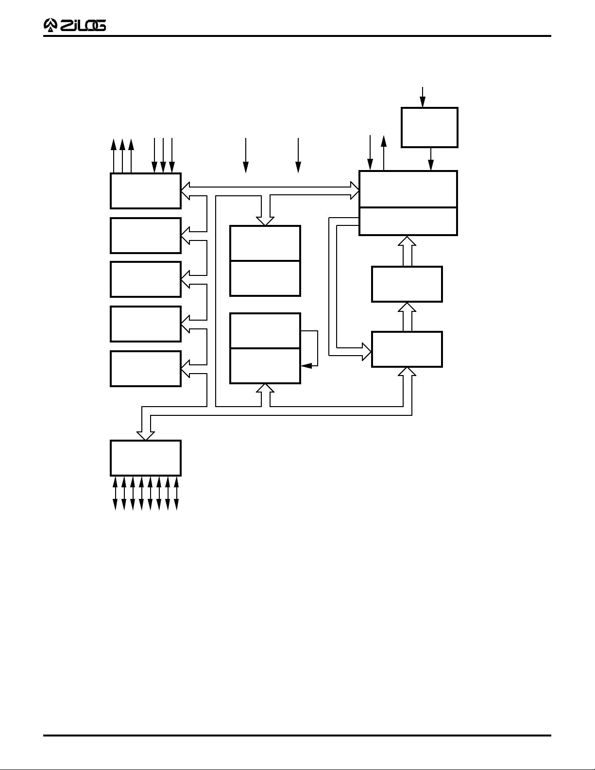
FUNCTIONAL DESCRIPTION
PRELIMINARY
Z86116
CP95WRL0501
TM BASE
InputOutput
Port 3
Counter/
Timers (2)
Interrupt
Control
T wo Analog
Comparators
PN
Modulator
VCC GND
ALU
FLAG
Register
Pointer
Register File
144 x 8-Bit
RC
Machine T iming &
Instruction Control
Time Base
Generator
WDT, POR
Prg. Memory
1024 x 8-Bit
Program
Counter
Port 2
I/O
(Bit Programmable)
Functional Block Diagram
2
PRELIMINARY
FUNCTIONAL DESCRIPTION (Continued)
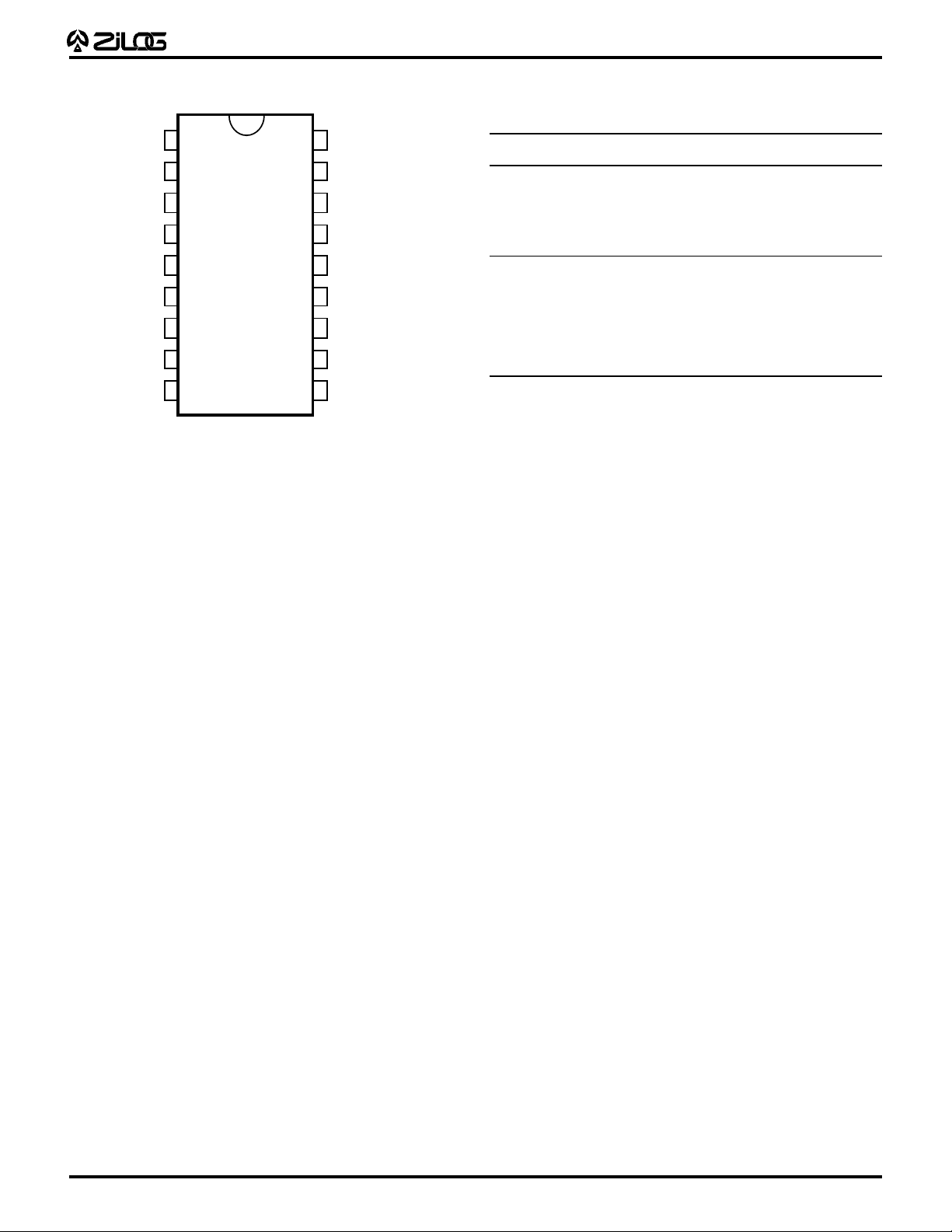
P24
P25
P26
P27
1
2
3
4
18
17
16
15
P23
P22
P21
P20
Z86116
CP95WRL0501
18-Pin DIP/SOIC Pin Identification
No Symbol Function Direction
1-4 P24-27 Port 2, Pins 4, 5, 6, 7 In/Output
5VCCPower Supply Input
6 RC2 RC Oscillator Clock Output
7 RC1 RC Oscillator Clock Input
Z86116
VCC
RC2
RC1
P31
P33
18-Pin DIP/SOIC Pin Configuration
5
6
7
8
9
14
13
12
11
10
GND
P36
P35
GND
TM BASE
8-9 P31, P33 Port 3, Pins 1, 3 Fixed Input
10 TM BASE Time Base Clock Input
11 GND Ground
12-13 P35-36 Port 3, Pins 5, 6 Fixed Output
14 GND Ground
15-18 P20-23 Port 2, Pins 0, 1, 2, 3 In/Output
3

ABSOLUTE MAXIMUM RATINGS
PRELIMINARY
Z86116
CP95WRL0501
Symbol Description Min Max Units
V
CC
T
STG
T
A
Notes:
* Voltage on all pins with respect to GND.
† See Ordering Information
Supply Voltage* –0.3 +7.0 V
Storage Temp –65 +150 C
Oper Ambient Temp † C
STANDARD TEST CONDITIONS
The characteristics listed below apply for standard test
conditions as noted. All voltages are referenced to ground.
Positive current flows into the referenced pin (Test Load
Configuration).
Stresses greater than those listed under Absolute Maximum Ratings may cause permanent damage to the device. This is a stress rating only; operation of the device at
any condition above those indicated in the operational
sections of these specifications is not implied. Exposure to
absolute maximum rating conditions for extended period
may affect device reliability.
+5V
2.1 K Ω
From Output
Under Test
150 pF 9.1 K Ω
Test Load Configuration
4

PRELIMINARY
DC ELECTRICAL CHARACTERISTICS
TA = 0°C to +70°C Typical
Sym Parameter V
CC
Min Max @ 25°C Units Conditions Notes
Z86116
CP95WRL0501
V
V
V
V
V
V
V
V
Max Input Voltage 3.0V 12 V I
≤ 250 µA
IN
5.5V 12 V IIN ≤ 250 µA
Clock Input High 3.0V 0.9 V
CH
V
CC
+0.3 2.4 V Driven by External Clock Generator
CC
Voltage
Clock Input Low 3.0V V
CL
5.5V 0.9 V
–0.3 0.2 V
SS
V
CC
+0.3 3.9 V Driven by External Clock Generator
CC
CC
1.6 V Driven by External Clock Generator
Voltage
5.5V V
Input High Voltage 3.0V 0.7 V
IH
5.5V 0.7 V
Input Low Voltage 3.0V V
IL
5.5V V
Output High Voltage 3.0V V
OH
5.5V V
Output Low Voltage 3.0V 0.8 0.2 V IOL = +4.0 mA
OL1
–0.3 0.2 V
SS
CC
CC
–0.3 0.2 V
SS
–0.3 0.2 V
SS
–0.4 3.1 V I
CC
–0.4 4.8 V IOH = –2.0 mA
CC
CC
V
+0.3 1.8 V
CC
V
+0.3 2.8 V
CC
CC
CC
2.7 V Driven by External Clock Generator
1.0 V
1.5 V
= –2.0 mA
OH
5.5V 0.4 0.1 V IOL = +4.0 mA
Output Low Voltage 3.0V 1.0 0.4 V IOL = 6 mA, 3 Pin Max
OL2
5.5V 1.0 0.5 V IOL = +12 mA, 3 Pin Max
Comparator Input 3.0V 25 10 mV
OFFSET
Offset Voltage 5.5V 25 10 mV
I
Input Leakage 3.0V –1.0 1.0 µAV
IL
(Input bias current 5.5V –1.0 1.0 µAV
= OV, V
IN
= OV, V
IN
CC
CC
of comparator)
I
I
Output Leakage 3.0V –1.0 1.0 µAV
OL
5.5V –1.0 1.0 µAV
Supply Current 3.0V 8.0 4.5 mA @ 12 MHz [2,3]
CC
= OV, V
IN
= OV, V
IN
CC
CC
5.5V 15 9.0 mA @ 12 MHz [2,3]
4.5V 15 10 µA 10 kHz; External RC [2,5]
5

PRELIMINARY
DC ELECTRICAL CHARACTERISTICS (Continued)
TA = 0°C to +70°C Typical
Sym Parameter V
I
Standby Current 3.0V 4.5 2.0 mA HALT mode VIN = OV, [2,3]
CC1
CC
(HALT Mode) V
5.5V 7.0 4.0 mA HALT mode VIN = OV, [2,3]
3.0V 2.0 1.0 mA Clock Divide-by-16 [2 3]
5.5V 4.5 2.5 mA Clock Divide-by-16 [2,3]
I
Standby Current 3.0V 10 1.0 µA STOP mode V
CC2
(STOP Mode) V
5.5V 10 3.0 µA STOP mode VIN = OV, [4]
3.0V TBD µA STOP mode VIN = OV, [4]
5.5V TBD 200 µA STOP mode VIN = OV, [4]
5.5V 12 5 µA STOP Mode; TM BASE = 32.768 KHz; [6]
Min Max @ 25°C Units Conditions Notes
@ 12 MHz
CC
VCC @ 12 MHz
@ 12 MHz
@ 12 MHz
= OV, [4]
WDT is not Running
CC
V
WDT is not Running
CC
V
WDT is Running
CC
IN
VCC WDT is Running
WDT is not Running
Z86116
CP95WRL0501
T
Power-On Reset 3.0V 7 24 13 ms
POR
5.5V 3 13 7 ms
V
VCC Low Voltage 1.50 2.65 2.1 V 2 MHz max Ext. CLK Freq. [1]
BO
Protection Voltage
Notes
[1] VLV increases as the temperature decreases.
[2] All outputs unloaded, I/O pins floating,
inputs at either rail, TM BASE clock input grounded.
[3] C
[4] Same as note [2] except inputs at VCC.
[5] Low EMI oscillator selected;
[6] Z8 in STOP mode;
= CL2 = 100 pF.
L1
SCLK = RC/2
RC selected for WDT;
10 kHz RC Oscillator
(corresponding to R ≈ 1.2 MΩ, C ≈ 68 pF).
WDT off;
TM BASE selected as Z8 system clock source
Time base counter enabled;
VCC = 5.5V.
6

PRELIMINARY
AC ELECTRICAL CHARACTERISTICS
Z86116
CP95WRL0501
Clock
TIN
IRQN
Clock
Setup
7 7
8
1
2 2 3
4
5
6
9
3
11
Stop-Mode
Recovery
Source
10
7

PRELIMINARY
AC ELECTRICAL CHARACTERISTICS (Continued)
TA = 0°C to +70°C
V
CC
No Sym Parameter Note [3] Min Max Units Notes
1 TpC Input Clock Period 3.3V 83 100,000 ns [1]
5.0V 83 100,000 ns [1]
2 TrC,TfC Clock Input Rise 3.3V 15 ns [1]
and Fall Times 5.0V 15 ns [1]
3 TwC Input Clock Width 3.3V 26 ns [1]
5.0V 26 ns [1]
4 TwTinL Timer Input Low Width 3.3V 100 ns [1]
5.0V 70 ns [1]
5 TwTinH Timer Input High Width 3.3V 3TpC [1]
5.0V 3TpC [1]
6 TpTin Timer Input Period 3.3V 8TpC [1]
5.0V 8TpC [1]
12 MHz
Z86116
CP95WRL0501
7 TrTin, Timer Input Rise 3.3V 100 ns [1]
TtTin and Fall Timer
5.0V 100 ns [1]
8 TwIL Int. Request Input 3.3V 100 ns [1,2]
Low Time
5.0V 70 ns [1,2]
9 TwIH Int. Request Input 3.3V 3TpC [1,2]
High Time
5.0V 3TpC [1,2]
10 Twsm Stop-Mode Recovery 3.3V 12 ns
Width Spec
5.0V 12 ns
11 Tost Oscillator Startup Time 3.3V 5TpC Reg.[4]
5.0V 5TpC ns
Twdt Watch-Dog Timer 3.3V 15 [5]
Refresh Time
5.0V 5 ms D0 = 0 [6, D1 = 0 [6]
3.3V 30 ms D0 = 1 [6]
5.0V 16 ms D1 = 0 [6]
3.3V 60 ms D0 = 0 [6]
5.0V 25 ms D1 = 1 [6]
3.3V 250 ms D0 = 1 [6]
5.0V 120 ms D1 = 1 [6]
Notes:
[1] Timing Reference uses 0.9 VCC for a logic 1 and 0.1 VCC for a logic 0.
[2] Interrupt request through Port 3 (P33-P31).
[3] 5.0V ±0.5V, 3.3V ±0.3V.
[4] SMR-D5 = 0.
[5] Reg. WDTMR.
[6] WDT Oscillator only.
8

PRELIMINARY
Z86116
CP95WRL0501
Pre-Characterization Product:
The product represented by this CPS is newly introduced
and Zilog has not completed the full characterization of the
product. The CPS states what Zilog knows about this
product at this time, but additional features or non-con-
© 1995 by Zilog, Inc. All rights reserved. No part of this document
may be copied or reproduced in any form or by any means
without the prior written consent of Zilog, Inc. The information in
this document is subject to change without notice. Devices sold
by Zilog, Inc. are covered by warranty and patent indemnification
provisions appearing in Zilog, Inc. Terms and Conditions of Sale
only. Zilog, Inc. makes no warranty, express, statutory, implied or
by description, regarding the information set forth herein or
regarding the freedom of the described devices from intellectual
property infringement. Zilog, Inc. makes no warranty of merchantability or fitness for any purpose. Zilog, Inc. shall not be
responsible for any errors that may appear in this document.
Zilog, Inc. makes no commitment to update or keep current the
information contained in this document.
formance with some aspects of the CPS may be found,
either by Zilog or its customers in the course of further
application and characterization work. In addition, Zilog
cautions that delivery may be uncertain at times, due to
start-up yield issues.
Zilog’s products are not authorized for use as critical components in life support devices or systems unless a specific written
agreement pertaining to such intended use is executed between
the customer and Zilog prior to use. Life support devices or
systems are those which are intended for surgical implantation
into the body, or which sustains life whose failure to perform,
when properly used in accordance with instructions for use
provided in the labeling, can be reasonably expected to result in
significant injury to the user.
Zilog, Inc. 210 East Hacienda Ave.
Campbell, CA 95008-6600
Telephone (408) 370-8000
Telex 910-338-7621
FAX 408 370-8056
Internet: http://www.zilog.com
9
 Loading...