

Page 1

eZ80® CPU
User Manual
UM007715-0415
Copyright © 2015 by Zilog®, Inc. All rights reserved.
www.zilog.com
Page 2

eZ80® CPU
Warning:
User Manual
DO NOT USE IN LIFE SUPPORT
LIFE SUPPORT POLICY
ZILOG'S PRODUCTS ARE NOT AUTHORIZED FOR USE AS CRITICAL COMPONENTS IN LIFE
SUPPORT DEVICES OR SYSTEMS WITHOUT THE EXPRESS PRIOR WRITTEN APPROVAL OF
THE PRESIDENT AND GENERAL COUNSEL OF ZILOG CORPORATION.
As used herein
Life support devices or systems are devices which (a) are intended for surgical implant into the body, or (b)
support or sustain life and whose failure to perform when properly used in accordance with instructions for
use provided in the labeling can be reasonably expected to result in a significant injury to the user. A
critical component is any component in a life support device or system whose failure to perform can be
reasonably expected to cause the failure of the life support device or system or to affect its safety or
effectiveness.
ii
Document Disclaimer
©2015 by Zilog, Inc. All rights reserved. Information in this publication concerning the devices,
applications, or technology described is intended to suggest possible uses and may be superseded. ZILOG,
INC. DOES NOT ASSUME LIABILITY FOR OR PROVIDE A REPRESENTATION OF ACCURACY
OF THE INFORMATION, DEVICES, OR TECHNOLOGY DESCRIBED IN THIS DOCUMENT.
ZILOG ALSO DOES NOT ASSUME LIABILITY FOR INTELLECTUAL PROPERTY
INFRINGEMENT RELATED IN ANY MANNER TO USE OF INFORMATION, DEVICES, OR
TECHNOLOGY DESCRIBED HEREIN OR OTHERWISE. The information contained within this
document has been verified according to the general principles of electrical and mechanical engineering.
Z8, Z8 Encore!, eZ80, Z8 Encore! XP, Z8 Encore! MC, Crimzon, and ZNEO are tradema rks or registered
trademarks of Zilog, Inc. All other product or service names are the property of their respective owners. .
UM007715-0415
Page 3

Revision History
Each instance in Revision History reflects a change to this document from its previous
revision. For more details, refer to the corresponding pages and appropriate links in the
table below.
Revision
Date
April 2015 15 Corrected the typo on Page 25 from '59h'
September
2008
Level Description Page Number
14 Change to new User Manual format All
eZ80® CPU
User Manual
iii
25
to '49h'.
UM007715-0415 Revision History
Page 4

Table of Contents
Manual Objectives . . . . . . . . . . . . . . . . . . . . . . . . . . . . . . . . . . . . . . . . . . . . . . . . . . .vi
About This Manual . . . . . . . . . . . . . . . . . . . . . . . . . . . . . . . . . . . . . . . . . . . . . . . . . . . . . . . . vi
Intended Audience . . . . . . . . . . . . . . . . . . . . . . . . . . . . . . . . . . . . . . . . . . . . . . . . . . . . . . . . . vi
Manual Organization . . . . . . . . . . . . . . . . . . . . . . . . . . . . . . . . . . . . . . . . . . . . . . . . . . . . . . .vi
Manual Conventions . . . . . . . . . . . . . . . . . . . . . . . . . . . . . . . . . . . . . . . . . . . . . . . . . . . . . . vii
Safeguards . . . . . . . . . . . . . . . . . . . . . . . . . . . . . . . . . . . . . . . . . . . . . . . . . . . . . . . . . . . . . . .ix
Introduction . . . . . . . . . . . . . . . . . . . . . . . . . . . . . . . . . . . . . . . . . . . . . . . . . . . . . . . . 1
Architectural Overview . . . . . . . . . . . . . . . . . . . . . . . . . . . . . . . . . . . . . . . . . . . . . . . 2
Processor Description . . . . . . . . . . . . . . . . . . . . . . . . . . . . . . . . . . . . . . . . . . . . . . . . . . . 2
Pipeline Description . . . . . . . . . . . . . . . . . . . . . . . . . . . . . . . . . . . . . . . . . . . . . . . . . . . . 3
eZ80® CPU
User Manual
iv
Memory Modes. . . . . . . . . . . . . . . . . . . . . . . . . . . . . . . . . . . . . . . . . . . . . . . . . . . . . . 6
Z80 MEMORY Mode . . . . . . . . . . . . . . . . . . . . . . . . . . . . . . . . . . . . . . . . . . . . . . . . . . . 6
ADL MEMORY Mode . . . . . . . . . . . . . . . . . . . . . . . . . . . . . . . . . . . . . . . . . . . . . . . . . . 7
Registers and Bit Flags. . . . . . . . . . . . . . . . . . . . . . . . . . . . . . . . . . . . . . . . . . . . . . . 9
®
eZ80
CPU Working Registers . . . . . . . . . . . . . . . . . . . . . . . . . . . . . . . . . . . . . . . . . . . 9
®
CPU Control Register Definitions . . . . . . . . . . . . . . . . . . . . . . . . . . . . . . . . . . . . 9
eZ80
®
eZ80
CPU Control Bits . . . . . . . . . . . . . . . . . . . . . . . . . . . . . . . . . . . . . . . . . . . . . . . . 10
®
eZ80
CPU Registers in Z80 Mode . . . . . . . . . . . . . . . . . . . . . . . . . . . . . . . . . . . . . . . 11
®
CPU Registers in ADL Mode . . . . . . . . . . . . . . . . . . . . . . . . . . . . . . . . . . . . . . 12
eZ80
®
eZ80
CPU Status Indicators (Flag Register) . . . . . . . . . . . . . . . . . . . . . . . . . . . . . . . . 14
Memory Mode Switching. . . . . . . . . . . . . . . . . . . . . . . . . . . . . . . . . . . . . . . . . . . . . 18
ADL Mode and Z80 Mode . . . . . . . . . . . . . . . . . . . . . . . . . . . . . . . . . . . . . . . . . . . . . . 18
Memory Mode Compiler Directives . . . . . . . . . . . . . . . . . . . . . . . . . . . . . . . . . . . . . . . 18
Opcode Suffixes for Memory Mode Control . . . . . . . . . . . . . . . . . . . . . . . . . . . . . . . . 18
Single-Instruction Memory Mode Changes . . . . . . . . . . . . . . . . . . . . . . . . . . . . . . . . . 20
Suffix Completion by the Assembler . . . . . . . . . . . . . . . . . . . . . . . . . . . . . . . . . . . . . . 24
Assembly of the Opcode Suffixes . . . . . . . . . . . . . . . . . . . . . . . . . . . . . . . . . . . . . . . . . 24
Persistent Memory Mode Changes in ADL and Z80 Modes . . . . . . . . . . . . . . . . . . . . 25
Mixed-Memory Mode Applications. . . . . . . . . . . . . . . . . . . . . . . . . . . . . . . . . . . . . 34
MIXED MEMORY Mode Guidelines . . . . . . . . . . . . . . . . . . . . . . . . . . . . . . . . . . . . . 34
Interrupts . . . . . . . . . . . . . . . . . . . . . . . . . . . . . . . . . . . . . . . . . . . . . . . . . . . . . . . . . 36
Interrupt Enable Flags (IEF1 and IEF2) . . . . . . . . . . . . . . . . . . . . . . . . . . . . . . . . . . . . 36
Interrupts in Mixed Memory Mode Applications . . . . . . . . . . . . . . . . . . . . . . . . . . . . . 36
®
eZ80
CPU Response to a Nonmaskable Interrupt . . . . . . . . . . . . . . . . . . . . . . . . . . . 37
®
eZ80
CPU Response to a Maskable Interrupt . . . . . . . . . . . . . . . . . . . . . . . . . . . . . . . 38
Vectored Interrupts for On-Chip Peripherals . . . . . . . . . . . . . . . . . . . . . . . . . . . . . . . . 43
UM007715-0415 Table of Contents
Page 5

eZ80® CPU
User Manual
Illegal Instruction Traps. . . . . . . . . . . . . . . . . . . . . . . . . . . . . . . . . . . . . . . . . . . . . . 46
I/O Space. . . . . . . . . . . . . . . . . . . . . . . . . . . . . . . . . . . . . . . . . . . . . . . . . . . . . . . . . . 47
Addressing Modes. . . . . . . . . . . . . . . . . . . . . . . . . . . . . . . . . . . . . . . . . . . . . . . . . . 48
v
CPU Instruction Set . . . . . . . . . . . . . . . . . . . . . . . . . . . . . . . . . . . . . . . . . . . . . . . . . 52
®
eZ80
CPU Assembly Language Programming Introduction . . . . . . . . . . . . . . . . . . . 52
®
CPU Instruction Notations . . . . . . . . . . . . . . . . . . . . . . . . . . . . . . . . . . . . . . . . . 53
eZ80
®
eZ80
CPU Instruction Classes . . . . . . . . . . . . . . . . . . . . . . . . . . . . . . . . . . . . . . . . . . 54
Instruction Summary . . . . . . . . . . . . . . . . . . . . . . . . . . . . . . . . . . . . . . . . . . . . . . . . . . . 59
®
CPU Instruction Set Description . . . . . . . . . . . . . . . . . . . . . . . . . . . . . . . . . . . . 77
eZ80
Opcode Maps . . . . . . . . . . . . . . . . . . . . . . . . . . . . . . . . . . . . . . . . . . . . . . . . . . . . . 375
Glossary . . . . . . . . . . . . . . . . . . . . . . . . . . . . . . . . . . . . . . . . . . . . . . . . . . . . . . . . . 382
Index . . . . . . . . . . . . . . . . . . . . . . . . . . . . . . . . . . . . . . . . . . . . . . . . . . . . . . . . . . . . 394
Customer Support . . . . . . . . . . . . . . . . . . . . . . . . . . . . . . . . . . . . . . . . . . . . . . . . . 402
UM007715-0415 Table of Contents
Page 6

Manual Objectives
This user manual describes the architecture and instruction set of the eZ80® CPU User
Manual.
About This Manual
Zilog recommends you to read all the chapters and instructions provided in this manual
before using the software.
Intended Audience
eZ80® CPU
User Manual
vi
This document is written for Zilog customers who are experienced at working with microcontrollers or in writing assembly code or compilers.
Manual Organization
The eZ80 CPU User Manual is divided into twelve sections; each section details a specific
topic about the product.
Introduction
This chapter provides an introduction to eZ80 CPU, Zilog’s next-generation processor
core.
Architectural Overview
This chapter provides an overview of eZ80 CPU’s features and benefits, and a description
of the eZ80 processor.
Memory Modes
This chapter describes eZ80’s two memory modes: ADL and Z80.
Registers and Bit Flags
This chapter provides register and bit descriptions for ADL and Z80 modes.
Memory Mode Switching
This chapter provides description of switching capability between ADL and Z80 modes.
UM007715-0415 Manual Objectives
Page 7

eZ80® CPU
User Manual
Interrupts
This chapter describes interrupt operation in maskable and nonmaskable mixed memory
modes.
Illegal Instruction Traps
This chapter describes the consequences of undefined operations.
I/O Space
This chapter describes input/output memory for on- and off-chip peripherals.
Addressing Modes
This chapter describes methods of accessing different addressing modes.
Mixed-Memory Mode Applications
vii
This chapter describes the MADL control bit and mixed memory mode guidelines.
CPU Instruction Set
This chapter lists assembly language instructions, including mnemonic definitions and a
summary of the eZ80
®
CPU instruction set.
Opcode Maps
This chapter provides a detailed diagram of each opcode segment.
Related Documents
eZ80190 eZ80190 Product Specification PS0066
eZ80190 Module Product Specification PS0191
eZ80L92 eZ80L92 Product Specification PS0130
eZ80L92 Module Product Specification PS0170
eZ80F92 eZ80F92 Product Specification PS0153
eZ80F92 Ethernet Module Product Specification PS0186
eZ80F92 Flash Module Product Specification PS0189
eZ80F91 eZ80F91 Product Specification PS0192
eZ80F91 Module Product Specification PS0193
Manual Conventions
The following conventions are used to provide clarity in the document.
UM007715-0415 Manual Objectives
Page 8

eZ80® CPU
User Manual
Courier Typeface
Commands, code lines and fragments, bits, equations, hexadecimal addresses, and various
executable items are distinguished from general text by the use of the
Where the use of the font is not indicated, as in the Index, the name of the entity is presented in upper case.
•
Example: FLAGS[1] is smrf.
Hexadecimal Values
Courier typeface.
viii
Hexadecimal values are designated by a lowercase h and appear in the
•
Example: STAT is set to F8h.
Brackets
The square brackets, [ ], indicate a register or bus.
•
Example: for the register REG1[7:0], REG1 is an 8-bit register, REG1[7] is the msb,
and REG1[0] is the lsb.
Braces
The curly braces, { }, indicate a single register or bus created by concatenating some combination of smaller registers, or buses.
•
Example: the 24-bit register {00h, REG1[7:0], REG2[7:0]} is composed of an 8-bit
hexadecimal value (
the 24-bit register, and REG2 is the LSB of the 24-bit register.
Parentheses
The parentheses, ( ), indicate an indirect register address lookup.
•
Example: (BC) is the memory location referenced by the address contained in the BC
register.
00h) and two 8-bit registers, REG1 and REG2. 00h is the MSB of
Courier typeface.
Parentheses/Bracket Combinations
The parentheses, ( ), indicate an indirect register address lookup and the square brackets, [
], indicate a register or bus.
•
Example: assume BC[15:0] contains the value 1234h. ({37h, BC[15:0]}) then refers
to the contents of the memory location at address
Use of the Words Set and Clear
The words set and clear imply that a register bit or a condition contains a logical 1 and a
logical 0, respectively. When either of these terms is followed by a number, the word logi-
cal may not be included; however, it is implied.
UM007715-0415 Manual Objectives
371234h.
Page 9

eZ80® CPU
User Manual
Use of the Terms LSB and MSB
In this document, the terms LSB and MSB, when appearing in upper case, mean least significant byte and most significant byte, respectively. The lowercase forms, msb and lsb,
mean least significant bit and most significant bit, respectively.
Use of Initial Uppercase Letters
Initial uppercase letters designate settings, modes, and conditions in general text.
•
Example 1: The Slave receiver leaves the data line High.
•
Example 2: The receiver forces the SCL line to Low.
•
Example 3: The Master can generate a Stop condition to abort the transfer.
Use of All Uppercase Letters
The use of all uppercase letters designates the names of states, modes, and commands.
ix
•
Example 1: The bus is considered BUSY after the Start condition.
•
Example 2: In TRANSMIT mode, the byte is sent most significant bit first.
•
Example 3: A START command triggers the processing of the initialization sequence.
Register Access Abbreviations
Register access is designated by the following abbreviations:
Designation Description
R Read Only
R/W Read/Write
W Write Only
— Unspecified or indeterminate
Bit Numbering
Bits are numbered from 0 to n–1.
Safeguards
It is important that you understand the following safety terms, which are defined here.
Caution:
UM007715-0415 Manual Objectives
Means a procedur e or file may become corrupted if you do not follow
directions.
Page 10

Introduction
Zilog’s eZ80® CPU is a high-speed, 8-bit microcontroller capable of executing code four
times faster than a standard Z80 operating at the same clock speed. The increased
processing efficiency of the eZ80 CPU improves available bandwidth and decrease power
consumption. The eZ80 CPU’s 8-bit processing power rivals the performance of
competitors’ 16-bit microcontrollers.
The eZ80 CPU is also the first 8-bit microcontroller to support 16 MB linear addressing.
Each software module, or each task, under a real-time executive or operating system can
operate in Z80-compatible (64 KB) mode or full 24-bit (16 MB) address mode.
The eZ80 CPU’s instruction set is a superset of the instruction sets for the Z80 and Z180
CPUs. The Z80 and Z180 programs are executed on an eZ80 CPU with little or no modification.
eZ80® CPU
User Manual
1
The eZ80 CPU is combined with peripherals, I/O devices, volatile and nonvolatile
memory, etc., for various eZ80 CPU products within the eZ80 and eZ80Acclaim!
product lines. Refer to the eZ80 and eZ80Acclaim!
information on these products.
1
®
product specifications for more
®
1. The term eZ80® CPU is referred to as CPU in this document.
UM007715-0415 Introduction
Page 11
Architectural Overview
The eZ80® CPU is Zilog's next-generation Z80 processor core. It is the basis of a new
family of integrated microcontrollers and includes the following features:
•
Upward code-compatible from Z80 and Z180 products.
•
Several address-generation modes, including 24-bit linear addressing.
•
24-bit registers and ALU.
•
8-bit data path.
•
Single-cycle fetch.
•
Pipelined fetch, decode, and execute.
eZ80® CPU
User Manual
2
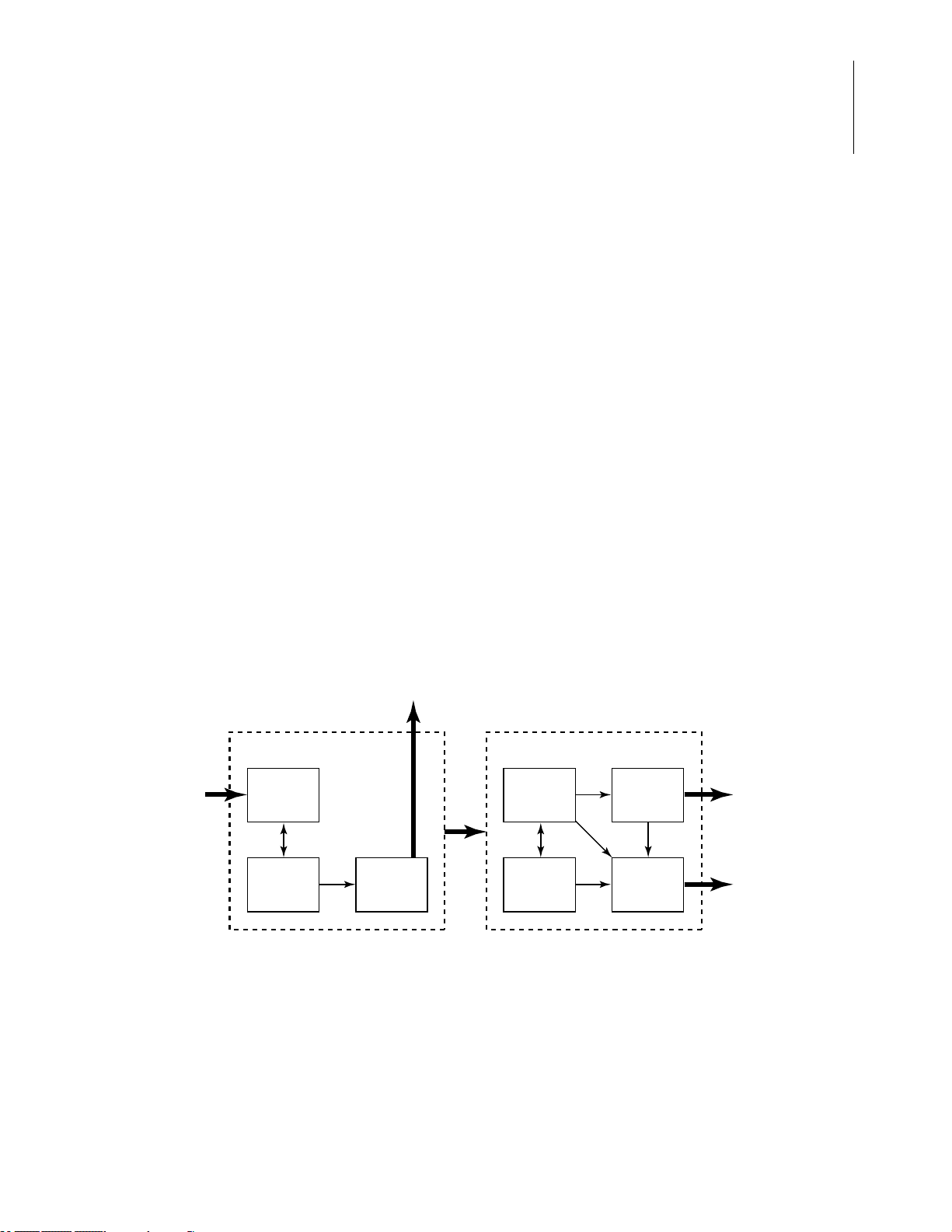
Processor Description
The eZ80® CPU is an 8-bit microcontroller that performs certain 16- or 24-bit operations.
A simplified block diagram of the CPU is displayed in Figure 1. Understanding the sepa-
ration between the control block and the data block is helpful toward understanding the
two eZ80
mode.
Control Block Data Block
DATA
®
memory modes—Z80 mode and ADDRESS AND DATA LONG (ADL)
Instruction
Fetch
Mode
Control
Figure 1. eZ80
I/O Control
Op Code
Decoder
CPU
Registers
ALU
®
CPU Block Diagram
Address
Generator
Data
Selector
ADDR
DATA
Instruction Fetch
The instruction fetch block contains a state machine which controls the READs from
memory. It fetches opcodes and operands and keeps track of the start and end of each
instruction. An instruction fetch block stores opcodes during external memory READs
UM007715-0415 Architectural Overview
Page 12

eZ80® CPU
User Manual
and WRITEs. It also discards prefetched instructions when jumps, interrupts, and other
control transfer events occur.
Mode Control
3
The Mode Control block of the CPU controls which mode the processor is currently operating in: HALT mode, SLEEP mode, Interrupt mode, debug mode, and ADL mode
1
.
Opcode Decoder
The opcodes are decoded within the CPU control block. After each instruction is fetched,
it is passed to the decoder. The opcode decoder is organized similarly to a large microcoded ROM.
CPU Registers
The CPU registers are contained within the CPU’s data block. Some are special purpose
registers, such as the Program Counter, the Stack Pointer, and the Flags register. There are
also a number of CPU control registers.
ALU
The arithmetic logic unit (ALU) is contained within the CPU’s data block. The ALU performs the arithmetic and logic functions on the addresses and the data passed over from
the control block or from the CPU
registers.
Address Generator
The address generator creates the addresses for all CPU memory READ and WRITE operations. The address generator also contains the Z80 Memory Mode Base Address register
(MBASE) for address translation in Z80 mode operation.
Data Selector
The data selector places the appropriate data onto the data bus. The data selector controls
the data path based on the instruction currently being executed.
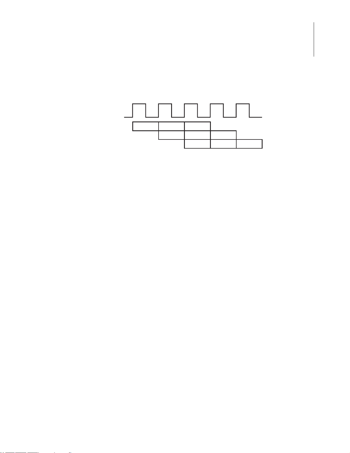
Pipeline Description
The CPU pipeline reduces the overall cycle time for each instruction. In principle, each
instruction must be fetched, decoded, and executed. This process normally spans at least
three cycles. The CPU pipeline, however, can reduce the overall time of some instructions
to as little as one cycle by allowing the next instruction to be prefetched and decoded
1. The debug interface is discussed in greater detail in the eZ80
product specification.
UM007715-0415 Architectural Overview
®
product specification and eZ80Acclaim!®
Page 13
eZ80® CPU
User Manual
while it executes the current instruction as displayed in Figure 2. The CPU operates on
multiple instructions simultaneously to improve operating efficiency.
System Clock
4
Instruction 1
Instruction 2
Instruction 3
Fetch Decode Execute
Fetch Decode Execute
Fetch Decode Execute
Figure 2. Pipeline Overview
In Figure 3, the pipelining process is demonstrated using a series of instructions. The first
LD
instruction prefetches its opcode and first operand during the decode and execute
phases of the preceding
INC
instruction. However, the second LD instruction in the
sequence only prefetches its opcode. The bus WRITE during the execute phase of the first
LD
instruction prevents the pipeline from prefetching the first operand of the next instruction. Thus, the number of bytes prefetched is a function of the command currently executing in the CPU.
When a control transfer takes place, the Program Counter (PC) does not progress sequentially. Therefore, the pipeline must be flushed. All prefetched values are ignored. Control
transfer can occur because of an interrupt or during execution of a Jump
RET
Return (
), Restart (
RST
), or similar instruction. After the control transfer instruction
(JP
),
CALL
,
is executed, the pipeline must start over to fetch the next operand.
UM007715-0415 Architectural Overview
Page 14

Clock
Address
PC
PC+1 PC+2 PC+3 PC+4 PC+5 PC+6 PC+7 5678h1234h
eZ80® CPU
User Manual
5
Data In
Command
Execution
State
LD (1234h), A
LD (5678h), A
Data Out
INST_READ
MEM_READ
MEM_WRITE
INC A LD (nn), A nL nH LD (nn), A Write nL nH INC A Write
INC A Fetch Decode
INC A
Note: F & D = Fetch & Decode
Prefetch
Next command
Execute
F & D F & D Decode
1 clock delay for execution
Execute
Prefetch
F & D F & D Decode
Figure 3. Pipeline Example
78h(1234h)32h12h (5678h)3Ch56h34h32h3Ch
1 clock delay for execution
Next command
Execute
Prefetch
ValidInvalidValidInvalid
UM007715-0415 Architectural Overview
Page 15

Memory Modes
The eZ80® CPU is capable of operating in two memory modes: Z80 mode and ADL
mode. For backward compatibility with legacy Z80 programs, the CPU operates in Z80
MEMORY mode with 16-bit addresses and 16-bit CPU registers. For 24-bit linear
addressing and 24-bit CPU registers, the CPU operates in ADDRESS AND DATA LONG
(ADL) mode. Selection of the memory mode is controlled by the ADL mode bit.
The multiple memory modes of the processor allow CPU products to easily mix existing
Z80 code or Z180 code with new ADL mode code. Collectively, the Z80 and ADL
memory modes may be referred to as ADL modes, because they are controlled by the
ADL bit.
Z80 MEMORY Mode
eZ80® CPU
User Manual
6
When the ADL bit is cleared to 0, the CPU operates using Z80-compatible addressing and
Z80-style, 16-bit CPU registers. This Z80 MEMORY mode is also occasionally referred to
as non-ADL mode. Z80 MEMORY mode is the default operating mode on reset.
In Z80 MEMORY mode (or its alternate term, Z80 mode), all of the multibyte internal
CPU registers are 16 bits. Also, the 16-bit Stack Pointer Short (SPS) register is used to
store the stack pointer value.
In addition, the CPU employs an 8-bit MBASE address register that is always prepended
to the 16-bit Z80 mode address. The complete 24-bit address is returned by {MBASE,
ADDR[15:0]}. The MBASE address register allows Z80 code to be placed anywhere
within the available 16 MB addressing space. This placement allows for 256 unique Z80
code blocks within the 16 MB address space, as displayed in Figure 4 on page 7.
UM007715-0415 Memory Modes
Page 16
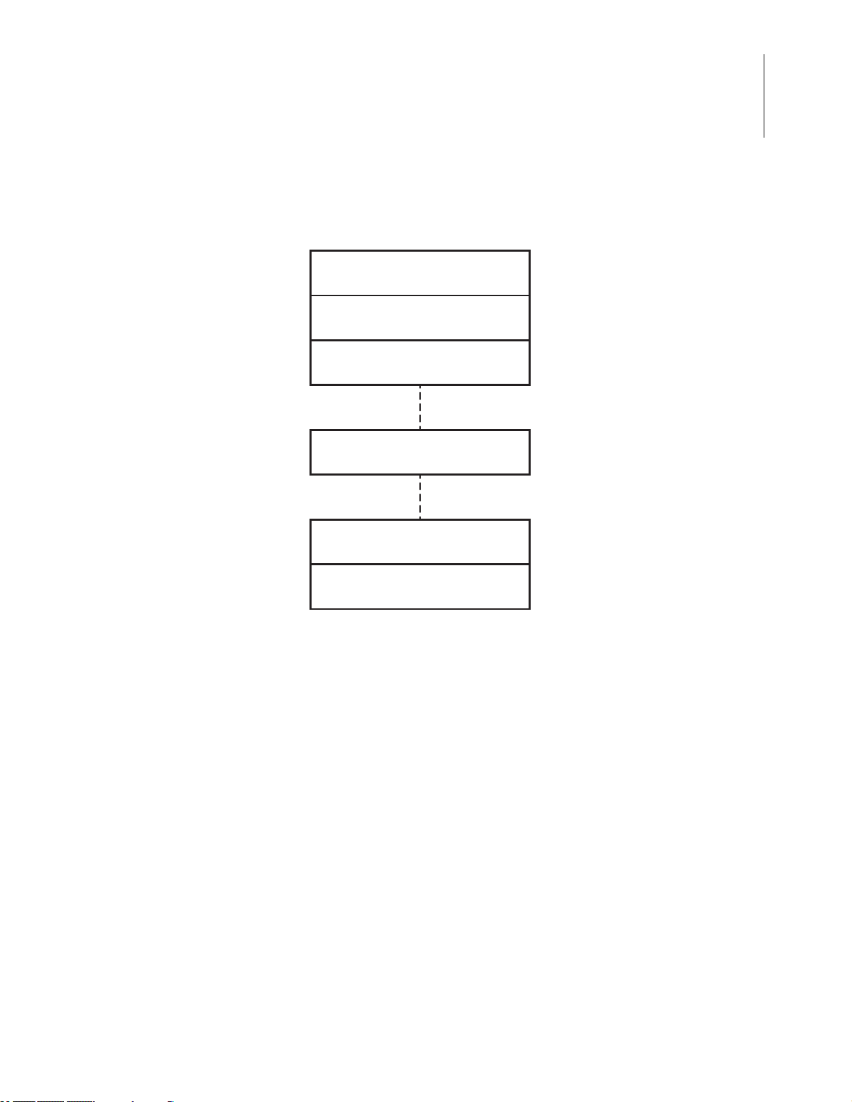
eZ80® CPU
User Manual
7
MBASE
00h
01h
02h
8Fh
FEh
FFh
Z80 Mode˜Page 0
64 KB
Z80 Mode˜Page 1
64 KB
Z80 Mode˜Page 2
64 KB
Z80 Mode˜Page 127
64 KB
Z80 Mode˜Page 254
64 KB
Z80 Mode˜Page 255
64 KB
Memory
Location
000000h
00FFFFh
010000h
01FFFFh
020000h
02FFFFh
8F0000h
8FFFFFh
FE0000h
FEFFFFh
FF0000h
FFFFFFh
Figure 4. Z80 MEMORY Mode Map
When MBASE is set to 00h, the CPU operates like a classic Z80 with
16-bit addressing from
bit Z80-style addresses are offset to a new page, as defined by MBASE.
By altering MBASE, multiple Z80 tasks can possess their own individual Z80 partitions.
The MBASE register can only be changed while in ADL mode, thereby preventing accidental page switching when operating in Z80 MEMORY mode. The MBASE address register does not affect the length of the CPU register. In Z80 mode, the CPU registers remain
16 bits, independent of the value of MBASE. For more information on the CPU registers
in Z80 mode, see the eZ80
ADL MEMORY Mode
Setting the ADL bit to 1 selects ADL mode. This memory mode is referred to as ADL
MEMORY mode or ADL mode. In ADL mode, the user application can take advantage of
the CPU’s 16 MB linear addressing space, 24-bit CPU registers, and enhanced instruction
0000h to 00FFh. When MBASE is set to a nonzero value, the 16-
®
CPU Registers in Z80 Mode on page 11.
UM007715-0415 Memory Modes
Page 17

eZ80® CPU
User Manual
set. When ADL mode is selected, MBASE does not affect memory addressing. Figure 5
displays the ADL mode memory map.
8
Note:
There are no pages in ADL mode.
24-Bit
Address
000000h
FFFFFFh
Figure 5. ADL Addressing Mode Memory Map
Memory
Location
000000h
ADL Mode
16 MB Linear
Memory Space
FFFFFFh
In ADL mode, the CPU’s multibyte registers are expanded from 16 to 24 bits. A 24-bit
Stack Pointer Long (SPL) register replaces the 16-bit Stack Pointer Short (SPS) register.
®
For more information on the CPU registers in ADL mode, see eZ80
CPU Registers in
ADL Mode on page 12.
In ADL mode, all addresses and data are 24 bits. All data READ and WRITE operations
pass 3 bytes of data to and from the CPU when operating in ADL mode (as opposed to
only 2 bytes of data while in Z80 mode operation). Thus, instructions operating in ADL
mode may require more clock cycles to complete than in Z80 mode. Although MBASE
does not affect operation during ADL mode, the MBASE register can only be written to
when operating in ADL mode.
UM007715-0415 Memory Modes
Page 18

Registers and Bit Flags
eZ80® CPU Working Registers
The CPU contains two banks of working registers—the main register set and the alternate
register set. The main register set contains the 8-bit accumulator register (A) and six 8-bit
working registers (B, C, D, E, H, and L). The six 8-bit working registers can be combined
to function as the multibyte register pairs BC, DE, and HL. The 8-bit Flag register F completes the main register set.
Similarly, the alternate register set also contains an 8-bit accumulator register (A’) and six
8-bit working registers (B’, C’, D’, E’, H’, and L’). These six 8-bit alternate working registers can also be combined to function as the multibyte register pairs BC’, DE’, and HL’.
The 8-bit Flag register F’ completes the alternate register set.
eZ80® CPU
User Manual
9
High-speed exchange between these two register banks is performed. See the EX and
EXX instructions on pages 143 through 147 for directions on exchanging register bank
contents. High-speed exchange between these banks can be used by a single section of
application code. Alternatively, the main program could use one register bank while the
other register banks are allocated to interrupt service routines.
eZ80® CPU Control Register Definitions
In addition to the two working register sets described in the previous section, the CPU
contains several registers that control CPU operation.
•
Interrupt Page Address Register (I)—the 16-bit I register stores the upper 16 bits of
the interrupt vector table address for Mode 2 vectored interrupts.
Note:
The 16-bit I register is not supported on eZ80190, eZ80L92, or eZ80F92/F93 devices.
•
Index Registers (IX and IY)—the multibyte registers IX and IY allow standard
addressing and relative displacement addressing in memory. Many instructions
employ the IX and IY registers for relative addressing in which an 8-bit two’s-comple-
d
ment displacement (
address. Additionally, certain 8-bit opcodes address the High and Low bytes of these
registers directly. For Index Register IX, the High byte is indicated by IXH, while the
Low byte is indicated by IXL. Similarly, for Index Register IY, the High byte is indicated by IYH, while the Low byte is indicated by IYL.
) is added to the contents of the IX or IY register to generate an
•
Z80 Memory Mode Base Address (MBASE) register—the 8-bit MBASE register
determines the page of memory currently employed when operating in Z80 mode. The
MBASE register is only used during Z80 mode. However, the MBASE register can
only be altered from ADL mode.
UM007715-0415 Registers and Bit Flags
Page 19

eZ80® CPU
User Manual
•
Program Counter (PC) register—the multibyte Program Counter register stores the
address of the current instruction being fetched from memory. The Program Counter is
automatically incremented during program execution. When a program jump occurs,
the new value is placed in the Program Counter, overriding the incremented value. In
Z80 mode, the Program Counter is only 16 bits; however, a full 24-bit address
{MBASE,PC[15:0]}, is used. In ADL mode, the Program Counter is returned by
{PC[23:0]}.
•
Refresh Counter (R) register—the Refresh Counter register contains a count of executed instruction fetch cycles. The 7 least significant bits (lsb) of the R register are
automatically incremented after each instruction fetch. The most significant bit (msb)
can only be changed by writing to the R register. The R register can be read from and
written to using dedicated instructions
•
Stack Pointer Long (SPL) register—in ADL mode, the 24-bit Stack Pointer Long
stores the address for the current top of the external stack. In ADL mode, the stack can
be located anywhere in memory. The external stack is organized as a last-in first-out
(LIFO) file. Data can be pushed onto the stack or popped off of the stack using the
PUSH and POP instructions. Interrupts, traps, calls, and returns also employ the
stack.
LD
A,R and LD R,A, respectively.
10
•
Stack Pointer Short register (SPS)—in Z80 mode, the 16-bit Stack Pointer Short stores
the address for the current top of the stack. In Z80 mode, the stack can be located anywhere within the current Z80 memory page. The current Z80 memory page is selected
by the MBASE register. The 24-bit Stack Pointer address in Z80 mode is {MBASE,
SPS}. The stack is organized as a last-in first-out (LIFO) file. Data can be pushed onto
the stack or popped off of the stack using the PUSH and POP instructions. Interrupts,
traps, calls, and returns also employ the stack.
eZ80® CPU Control Bits
•
Address and Data Long Mode Bit (ADL)—the ADL mode bit indicates the current
memory mode of the CPU. An ADL mode bit reset to 0 indicates that the CPU is operating in Z80 MEMORY mode with 16-bit Z80-style addresses offset by the 8-bit
MBASE register. An ADL mode bit set to 1 indicates that the CPU is operating in
ADL mode with 24-bit linear addressing. The default for the ADL mode bit is reset
(cleared to 0). The ADL mode bit can only be changed by those instructions that allow
persistent memory mode changes, interrupts, and traps. The ADL mode bit cannot be
directly written to.
•
Mixed-ADL Bit (MADL)—the MADL control bit is used to configure the CPU to
execute programs containing code that uses both ADL and Z80 MEMORY modes.
The MADL control bit is explained in more detail in Interrupts in Mixed Memory
Mode Applications on page 36. An additional explanation is available in the MixedMemory Mode Applications on page 34.
UM007715-0415 Registers and Bit Flags
Page 20
•
Interrupt Enable Flags (IEF1 and IEF2)—in the CPU, there are two interrupt enable
flags that are set or reset using the Enable Interrupt (EI) and Disable Interrupt (DI)
instructions. When IEF1 is reset to 0, a maskable interrupt cannot be accepted by the
CPU. The Interrupt Enable flags are described in more detail in Interrupts on page 36.
eZ80® CPU Registers in Z80 Mode
In Z80 mode, the BC, DE, and HL register pairs and the IX and IY
registers function as 16-bit registers for multibyte operations and indirect addressing. The
active Stack Pointer is the 16-bit Stack Pointer Short
register (SPS). The Program Counter register (PC) is also 16 bits long. The address is 24
bits long and is composed as {MBASE, ADDR[15:0]}. While the MBASE register is only
used during Z80 mode operations, it cannot be written while operating in this mode.
Tables 1 and 2 lists the CPU registers and bit flags during Z80 mode operation.
eZ80® CPU
User Manual
11
Caution:
Note:
In Z80 mode, the upper byte of the I register, bits [15:8], is not used.
In Z80 mode, the upper byte (bits 23:16) of each multibyte register is
undefined. When performing 16-bit operations with these registers, the
application program cannot assume values or behavior for the upper byte. The upper
byte is only valid in ADL mode.
Table 1. CPU Working Registers in Z80 Mode
Main Register Set Alternate Register Set
8-Bit
Registers
AA’
FF’
Individual
8-Bit
Registers
B C BC B’ C’ BC’
D E DE D’ E’ DE’
Or
16-Bit
Registers
8-Bit
Registers
Individual
8-Bit
Registers
16-Bit
Registers
Or
H L HL H’ L’ HL’
UM007715-0415 Registers and Bit Flags
Page 21
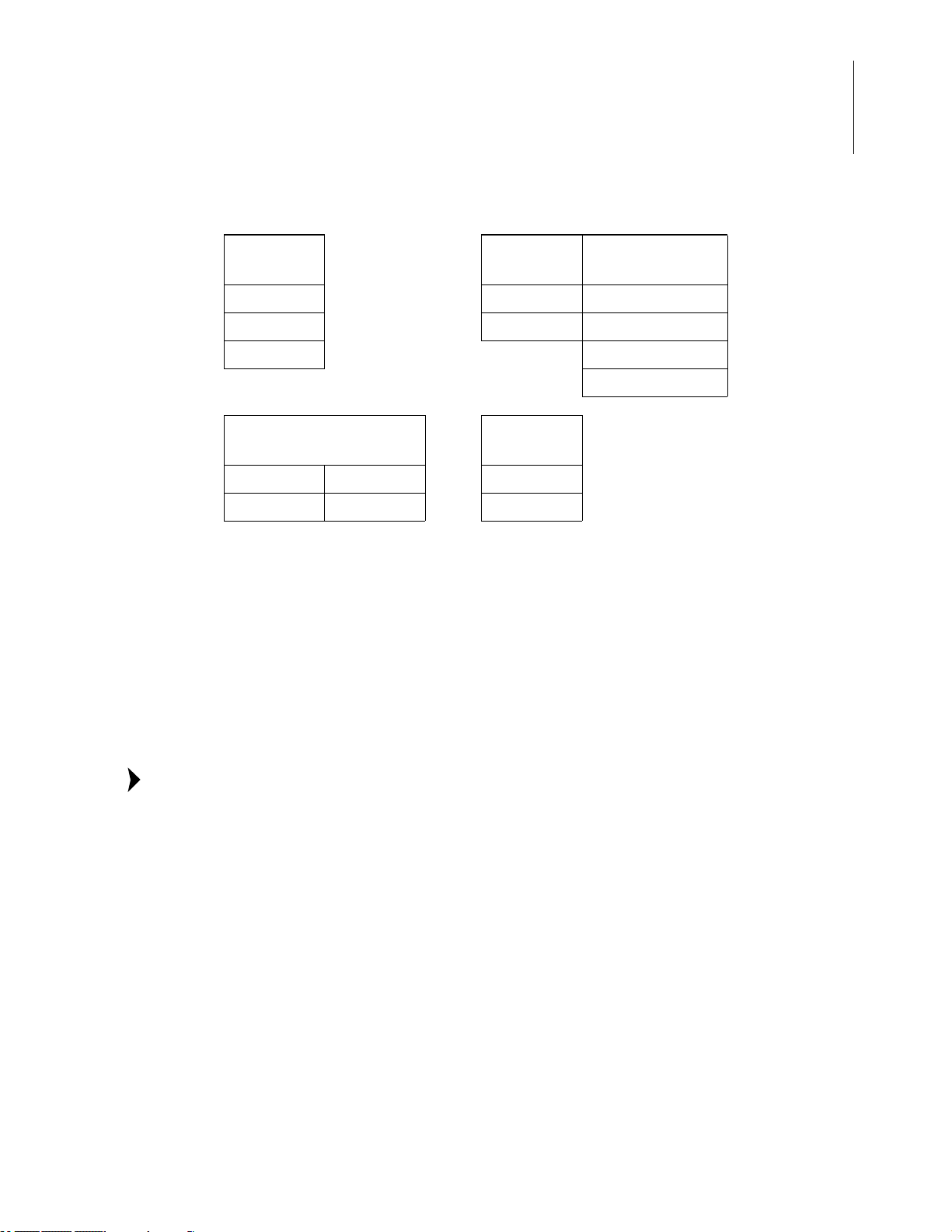
Table 2. CPU Control Registers and Bit Flags in Z80 Mode
eZ80® CPU
User Manual
12
8-Bit
Registers
I SPS ADL
MBASE PC MADL
RIEF1
Individual 8-Bit Registers
IXH IXL IX
IYH IYL IY
Or
eZ80® CPU Registers in ADL Mode
In ADL mode, the BC, DE, HL, IX and IY registers are 24 bits long for multibyte operations and indirect addressing. The most significant bytes (MSBs) of these 3 multibyte reg-
isters are designated with a U to indicate the upper byte. For example, the upper byte of
multibyte register BC is designated BCU. Thus, the 24-bit BC register in ADL mode is
composed of the three 8-bit registers {BCU, B, C}. Likewise, the upper byte of the IX register is designated IXU. The 24-bit IX register in ADL mode is composed of the three 8-bit
registers {IXU, IXH, IXL}.
16-Bit
Registers Single-Bit Flags
IEF2
16-Bit
Registers
Note:
None of the upper bytes (BCU, DEU, IXU, etc.) are individually accessible as standalone
8-bit registers.
MBASE is not used for address generation in ADL mode; however, it can only be written
in ADL mode. The Program Counter is 24 bits long, as is SPL. IEF1, IEF2, ADL, and
MADL are single bit flags.
The CPU registers and bit flags during Z80 mode operation are indicated in Tables 3 and
4. Reset states are detailed in Table 5.
UM007715-0415 Registers and Bit Flags
Page 22
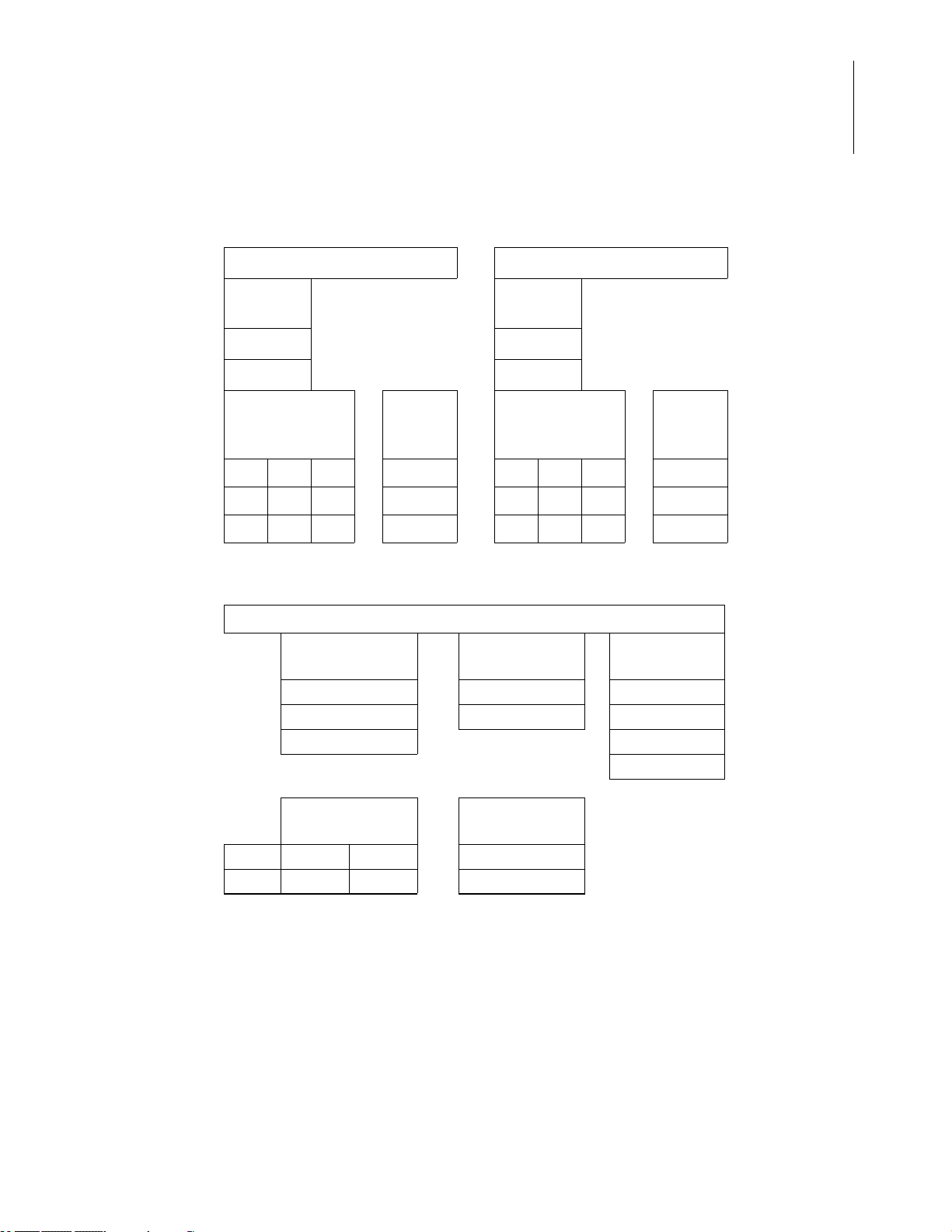
Table 3. CPU Working Registers in ADL Mode
Main Register Set Alternate Register Set
eZ80® CPU
User Manual
13
8-Bit
Registers
AA’
FF’
24-Bit
Individual
8-Bit Registers
BCU B C BC BCU’ B’ C’ BC’
DEU D E DE DEU’ D’ E’ DE’
HLU H L HL HLU’ H’ L’ HL’
Register
s
Or
8-Bit
Registers
Individual
8-Bit Registers
24-Bit
Register
s
Or
Table 4. CPU Control Registers and Bit Flags in ADL Mode
Control Registers and Bit Flags
Single-Bit
8-Bit Registers 24-Bit Registers
I SPL ADL
MBASE PC MADL
RIEF1
Flags
IEF2
Individual
8-Bit Registers
IXU IXH IXL IX
IYU IYH IYL IY
UM007715-0415 Registers and Bit Flags
24-Bit Registers
Or
Page 23

Table 5. CPU Register and Bit Flag Reset States
CPU Register
or Bit Flag Reset State
8-Bit Working Registers A, A’ Undefined
B, B’ Undefined
C, C’ Undefined
D, D’ Undefined
E, E’ Undefined
F, F’ Undefined
H, H’ Undefined
L, L’ Undefined
Upper Bytes of 24-Bit Multibyte
Working Registers
8-Bit Control Registers I 00h
Upper Bytes of 24-Bit Multibyte
Control Registers
16- and 24-Bit Control Registers PC 000000h
Single-Bit Flags ADL 0
BCU Undefined
DEU Undefined
HLU Undefined
IXH 00h
IXL 00h
IYH 00h
IYL 00h
MBASE 00h
R 00h
IXU 00h
IYU 00h
SPS 0000h
SPL 000000h
IEF1 0
IEF2 0
MADL 0
eZ80® CPU
User Manual
14
eZ80® CPU Status Indicators (Flag Register)
The Flag register (F and F’) contains status information for the CPU. The bit position for
each flag is indicated in Table 6 .
Table 6. Flag Register Bit Positions
Bit 76543210
Flag S Z XHXP/VNC
UM007715-0415 Registers and Bit Flags
Page 24

eZ80® CPU
User Manual
where:
C = Carry Flag
N = Add/Subtract Flag
P/V = Parity/Overflow Flag
H = Half-Carry Flag
Z = 0 Flag
S = Sign Flag
X = Not used
Each of the two CPU flag registers contain six bits of status information that are set or
reset by CPU operations. Bits 3 and 5 are not used. Four of these bits are testable (C, P/V,
Z and S) for use with conditional
jump, call
or
return
instructions. Two flags are not test-
able (H, N) and are used for BCD arithmetic.
Carry Flag (C)
15
The Carry Flag bit is set or reset, depending on the operation that is performed. For
instructions that generate a carry and
SUBTRACT
Carry flag is set to 1. The Carry flag is reset by an
instructions that generate a borrow, the
ADD
that does not generate a carry, and
ADD
a subtract that does not generate a borrow. This saved carry facilitates software routines
for extended precision arithmetic. Also, the
DAA
instruction sets the Carry flag to 1 if the
conditions for making the decimal adjustment are met.
For the
RLA, RRA, RLC
and
RRC
instructions, the Carry flag is used as a link between
the least significant bit (lsb) and most significant bit (msb) for any register or memory
location. During the
RLCA, RLC m
value shifted out of bit 7 of any register or memory location. During the
SRA m
and
SRL m
instructions, the carry contains the last value shifted out of bit 0 of
any register or memory location. For the logical instructions
A s
, the carry is reset. The Carry flag can also be set (
and
SLA m
instructions, the carry contains the last
RRCA, RRC m
AND A s, OR A s
SCF
) and complemented (
, and
CCF
XOR
).
Add/Subtract Flag (N)
The Add/Subtract (N) flag is used by the decimal adjust accumulator instructions (
ADD
and
to distinguish between
is set to 0. For all
SUBTRACT
SUBTRACT
instructions, N is set to 1.
instructions. For all
ADD
instructions, N
DAA
)
Parity/Overflow Flag (P/V)
The Parity/Overflow (P/V) flag is set or reset, depending on the operation that is performed. For arithmetic operations, this flag indicates an overflow condition when the
result in the accumulator is greater than the maximum possible number (+127) or is less
than the minimum possible number (–128). This overflow condition can be determined by
examining the sign bits of the operands.
,
UM007715-0415 Registers and Bit Flags
Page 25

eZ80® CPU
User Manual
For addition, operands with different signs never causes overflow. When adding operands
with like signs where the result yields a different sign, the overflow flag is set to 1, as indicated in Table 7 .
Table 7. Overflow Flag Addition Settings
+120 = 0111 10 00 ADDEND
+105 = 0110 10 01 AUGEND
+225 1110 0001 (–95) SUM
The two numbers added together result in a number that exceeds +127 and the two positive operands result in a negative number (–95), which is incorrect. Thus, the Overflow
flag is set to 1.
For subtraction, overflow can occur for operands of unlike signs. Operands of like signs
never causes overflow, as indicated in Table 8.
Table 8. Overflow Flag Subtraction Settings
16
+127 0111 1111 MINUEND
(–) –64 1100 0000 SUBTRAHEND
+191 1011 1111 DIFFERENCE
The minuend sign is changed from positive to negative, returning an incorrect difference.
Thus, overflow is set to 1. Another method for
predicting an overflow is to observe the carry into and out of the sign bit. If there is a carry
in and no carry out, then overflow occurs.
This flag is also used with logical operation and rotate instructions to
indicate the parity of the result. The number of 1 bits in a byte are counted. If the total is
odd, then odd parity (P = 0) is flagged. If the total is even, then even parity (P = 1) is
flagged.
During search instructions (
(
LDI, LDIR, LDD, LDDR
CPI, CPIR, CPD, CPDR
) and block transfer instructions
), the P/V flag monitors the state of the byte count register
(BC). When decrementing, the byte counter results in a 0 value and the flag is reset to 0;
otherwise the flag is logical 1.
During
LD A, I
and
LD A, R
instructions, the P/V flag is set to 1 with the contents of the
interrupt enable flip-flop (IEF2) for storage or testing. When inputting a byte from an I/O
device,
IN r,(C)
, the flag is adjusted to indicate the parity of the data.
The P/V flag is set to 1 to indicate even parity, and cleared to 0 to indicate odd parity.
UM007715-0415 Registers and Bit Flags
Page 26

eZ80® CPU
User Manual
Half-Carry Flag (H)
The Half-Carry flag (H) is set or reset, depending on the carry and borrow status between
bits 3 and 4 of an 8-bit arithmetic operation. This flag is used by the decimal adjust accumulator instruction (
DAA
) to correct the result of a packed BCD addition or subtraction.
The H flag is set to 1 or reset to 0, as indicated in Table 9.
Table 9. H Flag Settings
H ADD SUBTRACT
1 There is a carry from bit 3 to bit 4 There is a borrow from bit 4.
0 There is no carry from bit 3 to bit 4There is no borrow from bit 4.
Zero Flag (Z)
The Zero flag (Z) is set to 1 if the result generated by the execution of
certain instructions is 0. For 8-bit arithmetic and logical operations, the Z flag is set to 1 if
the resulting byte in the accumulator is 0. If the byte is not 0, the Z flag is reset to 0.
17
For compare instructions, the Z flag is set to 1 if the value in the
accumulator is the same as the data it is being compared against. When testing a bit in a
register or memory location, the Z flag contains the
complemented state of the indicated bit (see the
BIT b, r
instruction.
When inputting or outputting a byte between a memory location and an I/O device (for
example,
INI, IND, OUTI
and
OUTD
), the B register is decremented. If the result of this
decrement is 0 (that is, B–1 = 0), then the Z flag is set to 1. Otherwise, the Z flag is reset
(cleared to 0). Also, for byte inputs from I/O devices using
IN r,(C)
, the Z flag is set to 1 to
indicate a zero-byte input.
Sign Flag (S)
The Sign flag stores the state of the most significant bit of the
accumulator (bit 7). When the CPU performs arithmetic operations on signed numbers,
binary two’s-complement notation is used to represent and process numerical information.
A positive number is identified by a 0 in bit 7. A negative number is identified by a 1.
The binary equivalent of the magnitude of a positive number is stored in bits 0–6 for a
total range of 0–127. A negative number is represented by the two’s-complement of the
equivalent positive number. The total range for negative numbers is –1 to –128.
When inputting a byte from an I/O device to a register,
IN r,(C)
, the S flag indicates either
positive (S = 0) or negative (S = 1) data.
UM007715-0415 Registers and Bit Flags
Page 27

Memory Mode Switching
ADL Mode and Z80 Mode
The CPU is capable of easily switching between the two available memory modes (ADL
mode and Z80 mode). There are two types of mode changes available to the CPU: persistent and single-instruction. For example, persistent mode switches allow the CPU to operate indefinitely in ADL mode, then switch to Z80 mode to run a section of Z80 code, and
then return to ADL mode. Conversely, single-instruction mode changes allow certain
instructions to operate using either addressing mode without making a persistent change to
the mode.
Memory Mode Compiler Directives
eZ80® CPU
User Manual
18
In the Zilog ZMASM/ZDS assembler, the application code is assembled for a given state
of the ADL mode bit by placing one of the two following compiler directives at the top of
the code:
.ASSUME ADL = 1
.ASSUME ADL = 0
These compiler directives indicate that either ADL MEMORY mode (ADL = 1) or Z80
MEMORY mode (ADL = 0) is the default memory mode for the code being currently compiled. The code developer is responsible for ensuring that this source file setting matches
the state of the hardware ADL mode bit when the code is executed.
Opcode Suffixes for Memory Mode Control
When developing application code for CPU applications, care must be taken when manipulating the ADL and Z80 memory modes. Special opcode suffixes are added to the
instruction set to assist with memory mode switching operations. There are four individual
suffixes available for use:
many instructions to indicate that a memory mode change or an exception to standard
memory mode operation is being requested.
Even with the compiler directives described in the section Memory Mode Compiler
Directives on page 18, the code developer must still employ these opcode suffixes to allow
exceptions to the default memory mode. For example, the opcode suffixes can be used to
allow persistent memory mode switching between ADL and Z80 modes. In addition, there
may be times when ADL mode code may fetch a 16-bit address generated from a section
of Z80 mode code. Alternatively, a section of Z80 mode code may retrieve immediate data
created by a section of ADL mode code. The memory mode control suffixes facilitate
these requirements.
.SIS, .SIL, .LIS
, and
.LIL
. These suffixes are appended to
UM007715-0415 Memory Mode Switching
Page 28

eZ80® CPU
User Manual
19
Each of the four suffixes
.SIS, .SIL, .LIS
, and
.LIL
is composed of 2 parts that define the
operation in the control block and the data block within the CPU (see Figure 1 on page 2
and Tab l e 1 0 ). The first part of the suffix, either Short (
.S
within the data block of the CPU.
and .L control whether the overall operation of the
.S
) or Long (.L), directs operations
instruction and the internal registers should use 16 or 24 bits. The .S and .L portions of the
suffix also indicate if MBASE is used to define the 24-bit address. The last part of the suf-
.IS
or
.IL
fix, either
Short and Instruction Stream Long suffixes,
, directs the control block within the CPU. The Instruction Stream
.IS
and
.IL
, control whether a multibyte
immediate data or address value fetched during instruction execution is 2 or 3 bytes long
(for example, a
must know whether to fetch 3 bytes (
LD HL, Mmn
instruction versus a
Mmn
) or 2 bytes (mn) of data. The
LD HL, mn
instruction). The CPU
.IS
and
.IL
portions of the suffix tell the CPU the length of the instruction. If the length of the instruction
is unambiguous, the
.IS
and
.IL
suffixes yield no effect.
Table 10. Opcode Suffix Description
Suffix
Full Suffix
.SIS .S The CPU data block operates in Z80 mode using 16-bit
.SIL .S The CPU data block operates in Z80 mode using 16-bit
.LIS .L The CPU data block operates in ADL mode using 24-bit
.LIL .L The CPU data block operates in ADL mode using 24-bit
Components Description
registers. All addresses use MBASE.
.IS The CPU control block operates in Z80 mode. For
instructions with an ambiguous number of bytes, the .IS
suffix indicates that only 2 bytes of immediate data or
address must be fetched.
registers. All addresses use MBASE.
.IL The CPU control block operates in ADL mode. For
instructions with an ambiguous number of bytes, the .IL
suffix indicates that 3 bytes of immediate data or address
must be fetched.
registers. Addresses do not use MBASE.
.IS The CPU control block operates in Z80 mode. For
instructions with an ambiguous number of bytes, the .IS
suffix indicates that only 2 bytes of immediate data or
address must be fetched.
registers. Addresses do not use MBASE.
.IL The CPU control block operates in ADL mode. For
instructions with an ambiguous number of bytes, the .IL
suffix indicates that 3 bytes of immediate data or address
must be fetched.
UM007715-0415 Memory Mode Switching
Page 29

Single-Instruction Memory Mode Changes
Often, the CPU must perform a single operation using the memory mode opposite from
that currently set by the ADL mode bit. The CPU is capable of changing between ADL
mode and Z80 mode for a single instruction. Certain CPU instructions can be appended
with the memory mode opcode suffixes
ticular memory mode is appropriate for this instruction only. The following three examples serve to make the suffix operation for single-instruction memory mode changes more
clear.
.SIS, .LIL, .LIS
, and
eZ80® CPU
User Manual
.SIL
to indicate that a par-
20
Suffix Example 1: LD HL, Mmn in
In
Z80 mode (ADL mode bit = 0), only two bytes of immediate data are normally fetched
Z80 Mode
and the upper byte of all CPU multibyte registers is undefined. Compare the operation of
the following lines of code to observe the effect of the opcode suffixes.
.ASSUME ADL = 0 ;Z80 mode operation is default.
LD HL, 3456h ;HL[23:0] ¨ {00h, 3456h}.
LD HL, 123456h ;Invalid–Z80 mode cannot load 24-;bit value.
LD.SIS HL, 3456h ;Same as LD HL, 3456, because
;ADL = 0. HL[23:0] ¨ {00h, 3456h}.
;.IS directs eZ80 to fetch only
;16 bits of data.
;.S forces upper byte of HL
;register to an undefined state.
LD.LIL HL, 123456h ;HL[23:0] ¨ 123456h.
;.IL directs eZ80 to fetch 24;bits of data.
;.L uses all 3 bytes of HL
;register.
LD.LIS HL, 3456h ;HL[23:0] ¨ {00h, 3456h}. .IS
;directs eZ80 to fetch only 16;bits of data. .L uses all 3 bytes
;of HL register.
LD.SIL HL, 123456h ;HL[23:0] ¨ {00h, 3456h}.
;.IL directs eZ80 to fetch 24 bits
;of data. .S forces upper byte of
;HL register to an undefined
;state because registers are
;defined to be only 16-bits.
In all cases of Suffix Example 1, the memory mode is unchanged after the operation, as it
remains in Z80 mode (ADL mode bit = 0) following completion of each instruction. How-
ever, during operation of the LD.LIS, LD.LIL, and LD.SIL instructions, all or parts of
.IL
the CPU function temporarily in ADL mode. The
.L
trol block, to operate in ADL mode. The
segment of the suffix forces the data block to
segment of the suffix forces the con-
operate in ADL mode.
UM007715-0415 Memory Mode Switching
Page 30

eZ80® CPU
User Manual
Suffix Example 2: LD HL, Mmn in ADL Mode
Suffix Example 2 considers the same examples as in Suffix Example 1. However, for this
example, it is assumed that the part begins in ADL mode.
.ASSUME ADL = 1 ;ADL mode operation is default.
LD HL, 3456h ;HL[23:0] 003456h.
;3456h is valid 24-bit value.;Leading 0s are
assumed.
LD HL, 123456h ;HL[23:0] 123456h.
LD.SIS HL, 3456h ;HL[23:0] {00h, 3456h}.
;.IS directs the eZ80 to fetch
;only 16 bits of data.
;.S forces upper byte of the HL
;register to an undefined state.
LD.LIL HL, 123456h ;Same as LD HL, 123456h, because
;ADL = 1. HL[23:0] 123456h.
;.IL directs eZ80 to fetch 24
;bits of data.
;.L uses all 3 bytes of HL
;register.
LD.LIS HL, 3456h ;HL[23:0] {00h, 3456h}.
;.IS directs eZ80 to fetch only
;16 bits of data.
;.L uses all 3 bytes of HL
;register.
LD.SIL HL, 123456h ;HL[23:0] {00h, 3456h}.
;.IL directs eZ80 to fetch 24 bits
;of data.
.S forces upper byte of HL
;register to an undefined state.
21
From these two suffix examples, it can be seen that with the extensions applied, operation
is consistent regardless of the persistent memory mode in operation at the time. To
explain, a
rently operating in
LD.SIL
LD.LIS
, and
instruction operates in the same manner whether or not the CPU is cur-
Z80 mode or ADL mode. The same is also true for the
LD.LIL
instructions.
LD.SIS
,
Suffix Example 3: Risks with Using the .SIL Suffix
As Suffix Examples 1 and 2 demonstrate, special care must be taken when using the
.SIL
suffix. Wherever possible, the
the suffix (
.S
and
.IL
) are relevant. The
suffix should be avoided whenever both segments of
.IL
segment of the suffix indicates a long direct
.SIL
memory address or immediate data in the instruction stream and the CPU reads the 24-bit
.S
value. Because the
upper bits (23–16) that were read from the instruction are discarded (replaced with
is active, the internal registers are treated as 16-bit registers and the
00h).
Additionally, all memory WRITEs use Z80 mode employing MBASE. Therefore, the
upper byte of a 24-bit memory WRITE address is replaced by MBASE.
UM007715-0415 Memory Mode Switching
Page 31

eZ80® CPU
User Manual
LD.SIL HL, 123456h ;HL[23:0] {00h, 3456h}.
;.IL directs eZ80 to fetch 24 bits
;of data. .S forces upper byte of
;HL register to an undefined
;state. A different value is
;stored in HL than expected.
LD.SIL (123456h), HL;(3456h) HL.
;.IL forces a fetch of a 24-bit
;indirect address. .S forces Z80
;mode for writes to memory, thus
;address of write is {MBASE,
;3456h} rather than the address
;123456h that may be expected.
Suffix Example 4: LD (HL), BC in Z80 Mode
The following two examples, Suffix Example 4 and Suffix Example 5, further demonstrate how the suffixes affect internal CPU register operation and the creation of addresses.
In these two suffix examples, the .IS and .IL portions of the suffix have no effect because
the length of this instruction is unambiguous.
.ASSUME ADL = 0 ;Z80 Mode operation is default.
LD (HL), BC ;16-bit value stored in BC[15:0]
;is written to the 24-bit memory
;location given by
;{MBASE, HL[15:0]}.
LD.SIS (HL), BC ;16-bit value stored in BC[15:0]
;is written to the 24-bit memory
;location given by
;{MBASE, HL[15:0]}. The .S portion
;of the suffix has no effect since
;already operating in Z80 Mode.
;The .IS portion of the suffix has
;no effect since instruction
;length is unambiguous.
LD.LIL (HL), BC ;24-bit value stored in BC[23:0]
;is written to the 24-bit memory
;location given by HL[23:0]. The
;.L portion of the suffix forces
;the use of 24-bit registers and
;24-bit addresses without MBASE.
;The .IL portion of the suffix has
;no effect since instruction
;length is unambiguous.
LD.SIL (HL), BC ;16-bit value stored in BC[15:0]
;is written to the 24-bit memory
;location given by
;{MBASE,HL[15:0]}. The .S portion
;of the suffix has no effect since
22
UM007715-0415 Memory Mode Switching
Page 32

;already operating in Z80 Mode.
;The .IL portion of the suffix has
;no effect since instruction
;length is unambiguous.
LD.LIS (HL), BC ;24-bit value stored in BC[23:0]
;is written to the 24-bit memory
;location given by HL[23:0]. The
;.L portion of the suffix forces
;the use of 24-bit registers and
;24-bit addresses without
;MBASE.
;The .IS portion of the suffix has
;no effect since instruction
;length is unambiguous.
Suffix Example 5: LD (HL), BC in ADL Mode
eZ80® CPU
User Manual
23
.ASSUME ADL = 1 ;ADL Mode operation is default.
LD (HL), BC ;24-bit value stored in BC[23:0]
;is written to the 24-bit memory
;location given by HL[23:0].
LD.SIS (HL), BC ;16-bit value stored in BC[15:0]
;is written to the 24-bit memory
;location given by
;{MBASE,HL[15:0]}. The .S portion
;of the suffix forces the use of
;16-bit values from the registers
;and uses MBASE with the address.
;The .IS portion of the suffix has
;no effect since instruction
;length is unambiguous.
LD.LIL (HL), BC ;24-bit value stored in BC[23:0]
;is written to the 24-bit memory
;location given by HL[23:0].
;Since operating in ADL mode, the
;.L suffix has no effect on this
;instruction execution.
;The .IL portion of the suffix has
;no effect since instruction
;length is unambiguous.
LD.SIL (HL), BC ;16-bit value stored in BC[15:0]
;is written to the 24-bit memory
;location provided by
;{MBASE,HL[15:0]}. The .S
;portion of the suffix forces the
;use of 16-bit registers and MBASE
;with the address.
;The .IL portion of the suffix has
UM007715-0415 Memory Mode Switching
Page 33

;no effect because instruction
;length is unambiguous.
LD.LIS (HL), BC ;24-bit value stored in BC[23:0]
;is written to the 24-bit memory
;location given by HL[23:0].
;Because it is operating in ADL
;Mode, the.L portion of the suffix
;has no effect on this instruction
;execution.
;The .IS portion of the suffix has
;no effect because instruction
;length is unambiguous.
Suffix Completion by the Assembler
eZ80® CPU
User Manual
24
Ultimately, the assembler for the CPU creates one of the four full suffixes
.LIS
, or
.LIL
, depending on the current memory mode. Often, you are not required to
write the entire suffix. Partial suffixes (
or
.IL
is used by the code developer, the remainder of the full suffix is deduced from the
current memory mode state. The suffix completion by the assembler is listed in Tab l e 11.
Table 11. Opcode Suffix Completion by the Assembler
CPU Code
Partial Suffix ADL Mode Bit
.S 0 .SIS
.S 1 .SIL
.L 0 .LIS
.L 1 .LIL
.IS 0 .SIS
.IS 1 .LIS
.IL 0 .SIL
.IL 1 .LIL
Assembly of the Opcode Suffixes
.S, .L, .IS
, or
.IL
) can be employed. If .S,
Full Suffix Used
by CPU Assembler
.SIS, .SIL
.L, .IS
,
,
During assembly, the opcode suffixes become prefixes in the assembled code. The processor must know what type of memory mode exceptions must be applied to the instruction to
follow. The four assembled prefixes that correspond to the four full suffixes are displayed
in Table 12.
UM007715-0415 Memory Mode Switching
Page 34

eZ80® CPU
User Manual
Table 12. CPU Code Suffix to Assembled Prefix Mapping
Assembled Prefix Byte
CPU Code Suffix
.SIS 40
.LIS 49
.SIL 52
.LIL 5B
(hex)
The assembled prefix bytes replace Z80 and Z80180 instructions that do not offer a function. If an CPU assembler encounters one of these replaced instructions, it issues a warning message and assembles it as a standard NOP (
00h). The CPU prefix bytes are
indicated in Table 1 3.
25
Table 13. Z80 Instructions Replaced by Memory Mode Suffixes
Opcode Prefix
(hex)
40 LD B,B .SIS
49 LD C,C .LIS
52 LD D,D .SIL
5B LD E,E .LIL
Previous Z80 and Z180
Instruction New CPU Suffix
For the traditional Z80 prefix bytes, the CPU does not allow an interrupt to occur in the
time between fetching one of these prefix bytes and fetching the following instruction.
The traditional Z80 prefix bytes are
are not on the first page of the opcode map. The eZ80
(
40h, 49h, 52h, 5Bh) must precede the traditional Z80 prefix bytes.
CBh, DDh, EDh, and FDh, which indicate opcodes that
®
MEMORY mode prefix bytes
Persistent Memory Mode Changes in ADL and Z80 Modes
The CPU can only make persistent mode switches between ADL mode and Z80 mode as
part of a special control transfer instruction (CALL, JP, RST, RET, RETI, or RETN), or
as part of an interrupt or trap operation. The Program Counter (PC) is thus prevented from
making an uncontrolled jump. When the memory mode is changed in any of these ways, it
remains in its new state until another of these operations changes the mode back. Persistent mode changes are ideal for calling and executing a block of Z80-style code from
within a higher-level ADL mode program. Memory mode switching, using interrupts, and
traps are discussed in later sections of this manual.
UM007715-0415 Memory Mode Switching
Page 35

eZ80® CPU
User Manual
The memory mode can be changed by adding a suffix to a CALL, JP, RST, or RET,
RETI, or, RETN instruction. Tables 14 through 20 describe how each of these 4 instruc-
tions function. The individual instructions may perform additional operations that are not
described here. These tables are focused only on the memory mode switching. For more
®
detailed information, see eZ80
CPU Instruction Set Description on page 77.
Table 14. CALL Mmn Instruction
26
ADL
User Code
CALL mn 0 CALL mn
CALL Mmn 1 CALL Mmn
CALL.IS mn0 CALL.SIS mn
CALL.IS mn1 CALL.LIS mn
Mode
Assembled
Code Operation
assembles to
CD nn mm
assembles to
CD nn mm MM
assembles to
40 CD nn mm
assembles to
49 CD nn mm
The starting program counter is {MBASE,
PC[15:0]}. Push the 2-byte return address
PC[15:0] onto the SPS stack. The ADL mode bit
remains cleared to 0. Load 2-byte logical address
{mm, nn} from the instruction into PC[15:0]. The
ending program counter is {MBASE,
PC[15:0]} = {MBASE, mm, nn}.
The starting program counter is PC[23:0]. Push the
3-byte return address PC[23:0] onto the SPL
stack. The ADL mode bit remains set to 1. Load 3byte address {MM, mm, nn} from the instruction
into PC[23:0]. The ending program counter is
PC[23:0] = {MM, mm, nn}.
The starting program counter is {MBASE,
PC[15:0]}. Push the 2-byte logical return address
PC[15:0] onto the {MBASE, SPS} stack. Push a
02h byte onto the SPL stack, indicating a call from
Z80 mode, (because ADL = 0). The ADL mode bit
remains cleared to 0. Load 2-byte logical address
{mm, nn} from the instruction into PC[15:0]. The
ending program counter is {MBASE, PC[15:0]}.
The starting program counter is PC[23:0]. Push the
2 LS bytes of the return address, PC[15:0], onto
the {MBASE, SPS} stack. Push the MS byte of the
return address, PC[23:16], onto the SPL stack.
Push a 03h byte onto the SPL stack, indicating a
call from ADL mode (because ADL = 1). Reset the
ADL mode bit to 0. Load 2-byte logical address
{mm, nn} from the instruction into PC[15:0]. The
ending program counter is {MBASE,
PC[15:0]} = {MBASE, mm, nn}.
UM007715-0415 Memory Mode Switching
Page 36

Table 14. CALL Mmn Instruction (Continued)
eZ80® CPU
User Manual
27
User Code
CALL.IL
Mmn
CALL.IL
Mmn
ADL
Mode
0 CALL.SIL
1 CALL.LIL
Assembled
Code Operation
The starting program counter is {MBASE,
Mmn
assembles to
52 CD nn mm
MM
Mmn
assembles to
5B CD nn mm
MM
PC[15:0]}. Push the 2-byte logical return address,
PC[15:0], onto the SPL stack. Push a 02h byte
onto the SPL stack, indicating a call from Z80
mode (because ADL = 0). Set the ADL mode bit to
1. Load the 3-byte address {MM, mm, nn} from the
instruction into PC[23:0]. The ending program
counter is PC[23:0] = {MM, mm, nn}.
The starting program counter is PC[23:0]}. Push
the 3-byte return address, PC[23:0], onto the SPL
stack. Push a 03h byte onto the SPL stack,
indicating a call from ADL mode (because
ADL = 1). The ADL mode bit remains set to 1. Load
a 3-byte address {MM, mm, nn} from the
instruction into PC[23:0]. The ending program
counter is PC[23:0] = {MM, mm, nn}.
Table 15. JP Mmn Instruction
ADL
User Code
JP mn 0 JP mn
JP.SIS mn 0 JP.SIS mn
JP.LIL Mmn 0 JP.LIL mn
JP.SIL
Mmn
JP.LIS mn 0 N/A An illegal suffix for this instruction.
Mode
0 N/A An illegal suffix for this instruction.
Assembled
Code Operation
The starting program counter is {MBASE,
assembles to
C3 nn mm
assembles to
40 C3 nn mm
assembles to
5B C3 nn mm
PC[15:0]}. Write the 2-byte immediate value {mm,
nn}, to PC[15:0]. The ADL mode bit remains
cleared to 0. The ending program counter is
{MBASE, PC[15:0]} = {MBASE, mm, nn}.
This operation is the same as the previous
operation. The .SIS extension does not affect
operation when beginning in Z80 mode.
The starting program counter is {MBASE,
PC[15:0]}. Write the 3-byte immediate value {MM,
mm, nn}, to PC[23:0]. Set the ADL mode bit to 1.
The ending program counter is PC[23:0] = {MM,
mm, nn}.
UM007715-0415 Memory Mode Switching
Page 37

Table 15. JP Mmn Instruction (Continued)
eZ80® CPU
User Manual
28
ADL
User Code
JP Mmn 1 JP Mmn
JP.LIL Mmn 1 JP.LIL Mmn
JP.SIS mn 1 JP.SIS mn
JP.SIL
Mmn
JP.LIS mn 1 N/A An illegal suffix for this instruction.
Mode
1 N/A An illegal suffix for this instruction.
Because the CPU core resets to Z80 MEMORY mode, a
Assembled
Code Operation
The starting program counter is PC[23:0]. Write the
assembles to
C3 nn mm MM
assembles to
5B C3 nn mm
MM
assembles to
40 C3 nn mm
3-byte immediate value {MM, mm, nn}, to
PC[23:0]. The ADL mode bit remains set to 1. The
ending program counter is PC[23:0] = {MM, mm,
nn}.
This operation is the same as the previous
operation. The .LIL extension does not affect
operation when beginning in ADL mode.
The starting program counter is PC[23:0]. Write the
2-byte immediate value {mm, nn}, to PC[15:0].
Reset the ADL mode bit to 0. The ending program
counter is {MBASE, PC[15:0]} = {MBASE, mm, nn}.
JP.LIL Mmn
is recommended
for use near the beginning of source programs that run primarily in ADL MEMORY
mode.
Table 16. JP (rr) Instruction
ADL
User Code
JP (rr) 0 JP (rr)
JP.S (rr) 0 JP.SIS (rr)
JP.L (rr) 0 JP.LIS (rr)
UM007715-0415 Memory Mode Switching
Mode
Assembled
Code Operation
The starting program counter is {MBASE,
assembles to
E9 or DD/FD
E9
assembles to
40 E9 or 40
DD/FD E9
assembles to
49 E9 or
49 DD/FD E9
PC[15:0]}. Write the 2-byte value stored in rr[15:0]
to PC[15:0]. The ADL mode bit remains cleared to
0. The ending program counter is {MBASE,
PC[15:0]} = {MBASE, rr[15:0]}.
This operation is the same as the previous
operation. The .SIS extension does not affect
operation when beginning in Z80 mode.
The starting program counter is {MBASE,
PC[15:0]}. Write the 3-byte value stored in rr[23:0]
to PC[23:0]. Set the ADL mode bit to 1. The ending
program counter is PC[23:0] = rr[23:0].
Page 38

Table 16. JP (rr) Instruction (Continued)
eZ80® CPU
User Manual
29
ADL
User Code
JP (rr) 1 JP (rr)
JP.L (rr) 1 JP.LIL (rr)
JP.S (rr) 1 JP.SIL (rr)
Mode
Assembled
Code Operation
assembles to
E9 or DD/FD
E9
assembles to
5B E9 or
5B DD/FD E9
assembles to
52E9 or
52DD/FD E9
Table 17. RST n Instruction
ADL
User Code
RST n 0 RST n
RST n 1 RST n
RST.S n 0 RST.SIS n
Mode
Assembled
Code Operation
assembles to
CD nn
assembles to
CD nn
assembles to
40 CD nn
The starting program counter is PC[23:0]. Write the
3-byte value stored in rr[23:0] to PC[23:0]. The
ADL mode bit remains set to 1. The ending
program counter is PC[23:0] = rr[23:0].
This operation is the same as the previous
operation. The .LIL extension does not affect
operation when beginning in ADL mode.
The starting program counter is PC[23:0]. Write the
2-byte value stored in rr[15:0] to PC[15:0]. Reset
ADL mode bit to 0. The ending program counter is
{MBASE, PC[15:0]} = {MBASE, rr[15:0]}.
The starting program counter is {MBASE,
PC[15:0]}. Push the 2-byte return address,
PC[15:0], onto the {MBASE,SPS} stack. The ADL
mode bit remains cleared to 0. Write {00h, nn} to
PC[15:0]. The ending program counter is {MBASE,
PC[15:0]} = {MBASE, 00h, nn}.
The starting program counter is PC[23:0]. Push the
3-byte return address, PC[23:0], onto the SPL
stack. The ADL mode bit remains set to 1. Write
{0000h, nn} to PC[23:0]. The ending program
counter is PC[23:0] = {0000h, nn}.
The starting program counter is {MBASE,
PC[15:0]} Push the 2-byte return address,
PC[15:0], onto the {MBASE, SPS} stack. Push a
02h byte onto the SPL stack, indicating an
interrupt from Z80 mode (ADL = 0). The ADL mode
bit remains cleared to 0. Write {00h, nn} to
PC[15:0].The ending program counter is {MBASE,
PC[15:0]} = {MBASE, 00h, nn}.
UM007715-0415 Memory Mode Switching
Page 39

Table 17. RST n Instruction (Continued)
eZ80® CPU
User Manual
30
ADL
User Code
RST.S n 1 RST.SIL n
RST.L n 0 RST.LIS n
RST.L n 1 RST.LIL n
Mode
Assembled
Code Operation
assembles to
52 CD nn
assembles to
49 CD nn
assembles to
5B CD nn
The starting program counter is PC[23:0]. Push the
2 LS bytes of the return address, PC[15:0], onto
the {MBASE, SPS} stack. Push the MS byte of the
return address, PC[23:16], onto the SPL stack.
Push a 03h byte onto the SPL stack, indicating an
interrupt from ADL mode (because ADL = 1). Reset
ADL mode bit to 0. Write {00h, nn} to PC[15:0].
The ending program counter is {MBASE,
PC[15:0]} = {MBASE, 00h, nn}.
The starting program counter is {MBASE,
PC[15:0]}. Push the 2-byte return address,
PC[15:0], onto the SPL stack. Push a 02h byte
onto the SPL stack, indicating an interrupt from
Z80 mode (because ADL = 0). Set the ADL mode
bit to 1. Write {0000h, nn} to PC[23:0]. The ending
program counter is PC[23:0] = {0000h, nn}.
The starting program counter is PC[23:0]. Push the
3-byte return address, PC[23:0], onto the SPL
stack. Push a 03h byte onto the SPL stack,
indicating an interrupt from ADL mode (because
ADL = 1). The ADL mode bit remains set to 1. Write
{0000h, nn} to PC[23:0]. The ending program
counter is PC[23:0] = {0000h, nn}.
Table 18. RET Instruction
ADL
User Code
RET 0 RET
RET 1 RET
RET.S 0 — An invalid suffix. RET.L must be used in all mixed-
UM007715-0415 Memory Mode Switching
Mode
Assembled
Code Operation
The starting program counter is {MBASE,
assembles to
C9
assembles to
C9
PC[15:0]}. Pop a 2-byte return address from
{MBASE, SPS} into PC[15:0]. The ADL mode bit
remains cleared to 0. The ending program counter
is {MBASE, PC[15:0]}.
The starting program counter is PC[23:0]. Pop a 3byte return address from SPL into PC[23:0]. The
ADL mode bit remains set to 1. The ending
program counter is PC[23:0].
memory mode applications.
Page 40

Table 18. RET Instruction (Continued)
eZ80® CPU
User Manual
31
ADL
User Code
RET.S 1 — An invalid suffix. RET.L must be used in all mixed-
RET.L 0 RET.LIS
RET.L 1 RET.LIL
Mode
Assembled
Code Operation
memory mode applications.
The starting program counter is {MBASE,
assembles to
49 C9
assembles to
5B C9
PC[15:0]}. Pop a byte from SPL into ADL to set
memory mode (03h = A D L , 02h = Z 8 0 ) .
if ADL mode {
Pop the upper byte of the return address from SPL
into PC[23:16].
Pop 2 LS bytes of the return address from {MBASE,
SPS} into PC[15:0].
The ending program counter is PC[23:0].
}
else Z80 mode {
Pop a 2-byte return address from {MBASE,SPS}
into PC[15:0].
The ending program counter is {MBASE,
PC[15:0]}.
}
The starting program counter is PC[23:0]. Pop a
byte from SPL into ADL to set memory mode
(03h = ADL, 02h = Z80).
if ADL mode {
Pop 3-byte return address from SPL into PC[23:0].
The ending program counter is PC[23:0].
}
else Z80 mode {
Pop a 2-byte return address from SPL into PC[15:0].
The ending program counter is {MBASE,
PC[15:0]}.
}
Table 19. RETI Instruction
ADL
User Code
RETI 0 RETI
UM007715-0415 Memory Mode Switching
Mode
Assembled
Code Operation
The starting program counter is {MBASE,
assembles to
ED 4D
PC[15:0]}. Pop a 2-byte return address from
{MBASE, SPS} into PC[15:0]. The ADL mode bit
remains cleared to 0. The ending program counter
is {MBASE, PC[15:0]}.
Page 41

Table 19. RETI Instruction (Continued)
eZ80® CPU
User Manual
32
ADL
User Code
RETI 1 RETI
RETI.S 0 — Because RETI.S is an invalid suffix, RETI.L must
RETI.L 0 RETI.LIS
RETI.L 1 RETI.LIL
Mode
Assembled
Code Operation
The starting program counter is PC[23:0]. Pop a 3-
assembles to
ED 4D
assembles to
49 ED 4D
assembles to
5B ED 4D
byte return address from SPL into PC[23:0]. The
ADL mode bit remains set to 1. The ending
program counter is PC[23:0].
be used in all mixed-memory mode applications.
The starting program counter is {MBASE,
PC[15:0]}. Pop a byte from SPL into ADL to set
memory mode (03h = A D L , 02h = Z 8 0 ) .
if ADL mode {
Pop the upper byte of the return address from SPL
into PC[23:16].
Pop 2 LS bytes of the return address from {MBASE,
SPS} into PC[15:0].
The ending program counter is PC[23:0].
}
else Z80 mode {
Pop a 2-byte return address from {MBASE,SPS}
into PC[15:0]. The ending program counter is
{MBASE, PC[15:0]}.
}
The starting program counter is PC[23:0]. Pop a
byte from SPL into ADL to set memory mode
(03h = ADL, 02h = Z80).
if ADL mode {
Pop a 3-byte return address from SPL into PC[23:0].
The ending program counter is PC[23:0].
}
else Z80 mode {
Pop a 2-byte return address from SPL into PC[15:0].
The ending program counter is {MBASE,
PC[15:0]}.
}
UM007715-0415 Memory Mode Switching
Page 42

Table 20. RETN Instruction
eZ80® CPU
User Manual
33
ADL
User Code
RETN 0 RETN
RETN 1 RETN
RETN.S 0 — Because RETI.S is an invalid suffix, RETN.L must
RETN.L 0 RETN.LIS
RETN.L 1 RETN.LIL
Mode
Assembled
Code Operation
The starting program counter is {MBASE,
assembles to
ED 45
assembles to
ED 45
assembles to
49 ED 45
assembles to
5B ED 45
PC[15:0]}. Pop a 2-byte return address from
{MBASE, SPS} into PC[15:0]. The ADL mode bit
remains cleared to 0. The ending program counter
is {MBASE, PC[15:0]}. IEF1 IEF2.
The starting program counter is PC[23:0]. Pop a 3byte return address from SPL into PC[23:0]. The
ADL mode bit remains set to 1. The ending
program counter is PC[23:0]. IEF1 IEF2.
be used in all mixed-memory mode applications.
IEF1 IEF2.
The starting program counter is {MBASE,
PC[15:0]}. Pop a byte from SPL into ADL to set
memory mode (03h = A D L , 02h = Z 8 0 ) .
if ADL mode {
Pop the upper byte of the return address from SPL
into PC[23:16].
Pop 2 LS bytes of the return address from {MBASE,
SPS} into PC[15:0]. The ending program counter is
PC[23:0].
}
else Z80 mode {
Pop a 2-byte return address from {MBASE,SPS}
into PC[15:0]. The ending program counter is
{MBASE, PC[15:0]}. IEF1 IEF2.
}
The starting program counter is PC[23:0]. Pop a
byte from SPL into ADL to set memory mode
(03h = ADL, 02h = Z80).
if ADL mode {
Pop 3-byte return address from SPL into PC[23:0].
The ending program counter is PC[23:0].
}
else Z80 mode {
Pop a 2-byte return address from SPL into PC[15:0].
The ending program counter is {MBASE,
PC[15:0]}. IEF1 IEF2.
}
UM007715-0415 Memory Mode Switching
Page 43

Mixed-Memory Mode Applications
The eZ80® CPU contains a control bit flag that affects operation of interrupts, illegal
RST
instruction traps and restart (
must be set to 1 for all applications that run in both Z80 mode and ADL mode. The MADL
control bit can be reset to 0 for all CPU applications that run exclusively in Z80 mode or
exclusively in ADL mode. Default for the MADL control bit is reset to 0.
No application program can run exclusively in ADL mode, because the default for the
CPU is to begin in Z80 mode. If a single JP.LIL instruction is used at or near the begin-
ning of the source code to permanently change to ADL mode, this program is considered
to operate exclusively in ADL mode.
The purpose of the MADL control bit is to force the CPU to monitor the memory mode
when interrupts, traps or
then the MADL control bit can be reset to 0.
RST
) instructions. The Mixed-ADL (MADL) control bit
instructions occur. If the memory mode does not change,
eZ80® CPU
User Manual
34
When the MADL control bit is set to 1, the CPU pushes a byte onto the stack that contains
the current memory mode whenever an interrupt, trap, or restart occurs. Even if the memory mode is not changed by the current interrupt, trap, or restart, the byte containing the
memory mode bit is still pushed onto the stack. A
current code is operating in Z80 mode. A
code is operating in ADL mode. The current memory mode is pushed onto the stack prior
to setting the memory mode for the called service routine.
In addition, when the MADL control bit is set to 1 for mixed- memory mode applications,
all interrupts begin in ADL mode.
For applications that run exclusively in a single memory mode (either Z80 or ADL mode),
set the MADL control bit to 1. The CPU always handles interrupts, traps and restarts correctly if MADL is set to 1.
The MADL control bit is set to 1 by the STMIX instruction. The MADL control bit is
reset to 0 by the RSMIX instruction.
MIXED MEMORY Mode Guidelines
Applications that include legacy code that runs in Z80 mode, and new code that runs in
ADL mode, must follow certain rules to ensure proper operation:
1. Include a STMIX instruction in the device initialization procedure that sets MADL to
1, ensuring that interrupt service routines begin in a consistent memory mode (ADL
mode).
02h byte is pushed onto the stack if the
03h byte is pushed onto the stack if the current
2. End all interrupt service routines with a RETI.L or RETN.L instruction to ensure that
the interrupted code’s memory mode is popped from the SPL stack.
UM007715-0415 Mixed-Memory Mode Applications
Page 44

Note:
eZ80® CPU
User Manual
3. Use a suffixed CALL to access each block of code in the memory mode in which it
was assembled or compiled. Suffixed JP instructions may also be used; however, suffixed CALL instructions are recommended, because the CPU keeps track of all the
necessary memory modes when switching between blocks.
4. Any code block that may be called from either Z80 mode or ADL mode must be
called with a suffix to save the calling code’s memory mode on the SPL stack.
5. Any routine that may be called from either mode must return with a suffixed RETI.L
instruction to restore the calling code’s memory mode from the SPL stack.
6. If a calling code operating in one mode must pass stack-based operands/ arguments to
a routine compiled or assembled for a different mode, it must use suffixed instructions
.S
and
.L
to set up the operands/arguments. For PUSH,
suffixes control whether SPS
or SPL is used and whether the operands/ arguments are stored as 2- or 3-byte values.
In mixed-ADL applications, some of these rules may represent exceptions to the eZ80®
®
CPU’s design goal; that legacy code does not require modification to run on the eZ80
CPU. Assuming that legacy routines ar e not selectively converted to ADL mode and do not
call newly-written routines, the only rule that could lead to such modification is Rule 5. If
each legacy Z80 mode routine ends with a single RET.L at its end, this conversion is easy.
Internal and conditional RETs require more careful review.
35
UM007715-0415 Mixed-Memory Mode Applications
Page 45

Interrupt s
Interrupts allow peripheral devices to suspend CPU operation in an orderly manner and
force the CPU to start an interrupt service routine (ISR). Usually this interrupt service routine is involved with the exchange of data, status information, or control information
between the CPU and the interrupting peripheral. When the service routine is completed,
the CPU returns to the operation from which it was interrupted.
The CPU respond to two different interrupt types—maskable interrupts and nonmaskable
interrupts. The nonmaskable interrupt (NMI) cannot be disabled by the programmer. An
NMI request is always accepted when the peripheral device requests it. You can enable or
disable maskable interrupts.
Interrupt Enable Flags (IEF1 and IEF2)
eZ80® CPU
User Manual
36
In the eZ80® CPU, there are two interrupt enable flags (IEF1 and IEF2) that are set or
reset using the Enable Interrupt (EI) and Disable Interrupt (DI) instructions. When IEF1 is
reset to 0 by a DI instruction, a maskable interrupt cannot be accepted by the CPU. When
IEF1 is set to 1 by an EI instruction, a maskable interrupt is acknowledged by the CPU
and executed.
The state of IEF1 is used to enable or inhibit interrupts, while IEF2 is used as a temporary
storage location for IEF1. At reset, the CPU clears both IEF1 and IEF2 to 0, which dis-
ables the maskable interrupts. The maskable interrupts can be enabled using the EI
instruction. No pending interrupt is accepted until the instruction that follows the EI
instruction is executed. The single instruction delay occurs because EI is often followed
by a return instruction, and because interrupts must not be allowed until the return is complete.
When a maskable interrupt is accepted by the CPU, both IEF1 and IEF2 are reset to the
disabled state, thus inhibiting further interrupts until a new EI instruction is executed. For
all of the cases discussed previously in this section, IEF1 and IEF2 are always equal.
The purpose of IEF2 is to save the status of IEF1 when a nonmaskable interrupt occurs.
When a nonmaskable interrupt is accepted, IEF1 is reset to prevent further interrupts until
reenabled by the application code. The status of IEF1 is restored by executing the Return
From Nonmaskable (RETN) instruction. During execution of a Return From Nonmaskable Interrupt, the CPU copies the contents of IEF2 back into IEF1. In addition, the LD
A,I or LD A,R instructions copy the state of IEF2 into the Parity flag where it can be
tested or stored.
Interrupts in Mixed Memory Mode Applications
For all mixed-memory mode applications, the MADL control bit must be set to 1 using the
STMIX instruction. When the MADL is set to 1, all interrupt service routines (ISRs)
UM007715-0415 Interrupts
Page 46

begin in ADL mode. To explain, the ADL mode bit is set to 1 and full 24-bit linear
addressing is used to access the ISRs. The ADL mode bit setting of the interrupted code is
pushed onto the stack, using SPL, to allow the memory mode to return to the appropriate
value after completion of the ISR. For mixed-memory mode applications, all ISRs must
end with either a RETI.L for maskable interrupts or RETN.L for nonmaskable interrupts.
eZ80® CPU Response to a Nonmaskable Interrupt
The CPU always accepts a nonmaskable interrupt (NMI). The state of the Interrupt Enable
flags (IEF1 and IEF2) have no effect on nonmaskable interrupt operation. CPU operation
in response to an NMI is described in detail in Tab l e 2 1 .
Table 21. Nonmaskable Interrupt Operation
eZ80® CPU
User Manual
37
ADL
Current
Memory Mode
Z80 mode 0 0
ADL mode 1 0
Z80 mode 0 1
Mode
Bit
MADL
Control
Bit Operation
IEF2 IEF1
IEF1 0
The starting program counter is {MBASE, PC[15:0]}.
Push the 2-byte return address, PC[15:0], onto the
{MBASE,SPS} stack. The ADL mode bit remains
cleared to 0. Write 0066h to PC[15:0]. The ending
program counter is {MBASE, PC[15:0]} = {MBASE,
0066h}. The interrupt service routine must end with
RETN.
IEF2 IEF1
IEF1 0
The starting program counter is PC[23:0]. Push the 3byte return address, PC[23:0], onto the SPL stack. The
ADL mode bit remains set to 1. Write 000066h to
PC[23:0]. The ending program counter is
PC[23:0] = 000066h. The interrupt service routine must
end with RETN.
IEF2 IEF1
IEF1 0
The starting program counter is {MBASE, PC[15:0]}.
Push the 2-byte return address, PC[15:0], onto the
SPL stack. Push a 02h byte onto the SPL stack,
indicating interrupting from Z80 mode (because
ADL = 0). Set the ADL mode bit to 1. Write 000066h to
PC[23:0]. The ending program counter is
PC[23:0] = 000066h. The interrupt service routine must
end with RETN.L.
UM007715-0415 Interrupts
Page 47

Table 21. Nonmaskable Interrupt Operation (Continued)
eZ80® CPU
User Manual
38
ADL
Current
Memory Mode
ADL mode 1 1
Mode
Bit
MADL
Control
Bit Operation
IEF2 IEF1
IEF1 0
The starting program counter is PC[23:0]. Push the 3byte return address, PC[23:0], onto the SPL stack.
Push a 03h byte onto the SPL stack, indicating an
interrupt from ADL mode (because ADL = 1). The ADL
mode bit remains set to 1. Write 000066h to PC[23:0].
The ending program counter is PC[23:0] = 000066h.
The interrupt service routine must end with RETN.L.
eZ80® CPU Response to a Maskable Interrupt
The eZ80® CPU is capable of responding to a maskable interrupt using one of three interrupt modes: Interrupt Mode 0, Interrupt Mode 1, or Interrupt Mode 2. The maskable interrupt mode is set by the IM 0, IM 1, and IM 2 instructions. Not all products within the
®
family support all 3 of these interrupt modes. Refer to the eZ80® and
eZ80
eZ80Acclaim!
Interrupt Mode 0
®
product specifications for information on supported interrupt modes.
In Interrupt Mode 0, the interrupting device places the appropriate instruction onto the
data bus during the interrupt acknowledge cycle. Interrupt Mode 0 is the default state upon
reset of the CPU. Interrupt Mode 0 is also selected by execution of the IM 0 instruction.
The instruction placed on the data bus must be a single byte restart instruction, RST n,
with binary value
tion with binary value
C7h, CFh, D7h, DFh, E7h, EFh, F7h, or FFh, or a CALL Mmn instruc-
CDh. If any other binary value is placed on the data bus during the
interrupt acknowledge cycle, the CPU treats the instruction as a NOP. The binary opcodes
corresponding to the memory mode suffixes (
.SIS, .LIL, .SIL
, or
.LIS
) cannot be placed
on the data bus by the interrupting peripheral.
UM007715-0415 Interrupts
Page 48

Table 22. Interrupt Mode 0 Operation
eZ80® CPU
User Manual
39
ADL
Current
Memory Mode
Z80 mode 0 0 Read the RST n of CALL mn instruction placed on the
ADL mode 1 0 Read RST n or CALL Mmn instruction placed on the
Z80 mode 0 1 Read RST n or CALL Mmn instruction placed on the
Mode
Bit
MADL
Control
Bit
Operation (if RST n or CALL Mmn is placed on the
data bus)
data bus, D[7:0], by the interrupting peripheral.
IEF1 0
IEF2 0
The starting program counter is {MBASE, PC[15:0]}.
Push the 2-byte return address, PC[15:0], onto the
{MBASE,SPS} stack. The ADL mode bit remains
cleared to 0. Write {00h, nn} or {mm, nn} to PC[15:0].
The ending program counter is {MBASE,
PC[15:0]} = {MBASE, 00h, nn} or {MBASE, mm, nn}.
The interrupt service routine must end with RETI.
data bus, D[7:0], by the interrupting peripheral.
IEF1 0
IEF2 0
The starting program counter is PC[23:0]. Push the 3byte return address, PC[23:0], onto the SPL stack. The
ADL mode bit remains set to 1. Write {0000h, nn} or
{MM, mm, nn} to PC[23:0]. The ending program
counter is PC[23:0] = {0000h, nn} or {MM, mm, nn}.
The interrupt service routine must end with RETI.
data bus, D[7:0], by interrupting peripheral.
IEF1 0
IEF2 0
The starting program counter is {MBASE, PC[15:0]}.
Push the 2-byte return address, PC[15:0], onto the
SPL stack. Push a 02h byte onto the SPL stack,
indicating interrupting from Z80 mode (because
ADL = 0). Set the ADL mode bit to 1. Write {0000h, nn}
or {MM, mm, nn} to PC[23:0]. The ending program
counter is PC[23:0] = {0000h, nn} or {MM, mm, nn}.
The interrupt service routine must end with RETI.L
UM007715-0415 Interrupts
Page 49

Table 22. Interrupt Mode 0 Operation (Continued)
eZ80® CPU
User Manual
40
ADL
Current
Memory Mode
ADL mode 1 1 Read RST n or CALL Mmn instruction placed on the
Mode
Bit
MADL
Control
Bit
Operation (if RST n or CALL Mmn is placed on the
data bus)
data bus, D[7:0], by interrupting peripheral.
IEF1 0
IEF2 0
The starting program counter is PC[23:0]. Push the 3byte return address, PC[23:0], onto the SPL stack.
Push a 03h byte onto the SPL stack, indicating an
interrupt from ADL mode (because ADL = 1). The ADL
mode bit remains set to 1. Write {0000h, nn} or {MM,
mm, nn} to PC[23:0]. The ending program counter is
PC[23:0] = {0000h, nn} or {MM, mm, nn}. The interrupt
service routine must end with RETI.L
Interrupt Mode 1
In Interrupt Mode 1, the CPU responds to an interrupt by executing a restart to location
0038h (
RST
38h). Interrupt Mode 1 is selected by executing a IM 1 instruction.
Table 23. Interrupt Mode 1 Operation
ADL
Current
Memory Mode
Z80 mode 0 0
ADL mode 1 0
Mode
Bit
MADL
Control
Bit Operation
IEF1 0
IEF2 0
The starting program counter is {MBASE, PC[15:0]}.
Push the 2-byte return address, PC[15:0], onto the
{MBASE,SPS} stack. The ADL mode bit remains
cleared to 0. Write 0038h to PC[15:0]. The ending
program counter is {MBASE, PC[15:0]} = {MBASE,
0038h} The interrupt service routine must end with
RETI.
IEF1 0
IEF2 0
The starting program counter is PC[23:0]. Push the 3byte return address, PC[23:0], onto the SPL stack. The
ADL mode bit remains set to 1. Write 000038h to
PC[23:0]. The ending program counter is
PC[23:0] = 000038h. The interrupt service routine must
end with RETI.
UM007715-0415 Interrupts
Page 50

Table 23. Interrupt Mode 1 Operation (Continued)
eZ80® CPU
User Manual
41
ADL
Current
Memory Mode
Z80 mode 0 1
ADL mode 1 1
Mode
Bit
MADL
Control
Bit Operation
IEF1 0
IEF2 0
The starting program counter is {MBASE, PC[15:0]}.
Push the 2-byte return address, PC[15:0], onto the
SPL stack. Push a 02h byte onto the SPL stack,
indicating interrupting from Z80 mode (because
ADL = 0). Set the ADL mode bit to 1. Write 000038h to
PC[23:0]. The ending program counter is
PC[23:0] = 000038h. The interrupt service routine must
end with RETI.L.
IEF1 0
IEF2 0
The starting program counter is PC[23:0]. Push the 3byte return address, PC[23:0], onto the SPL stack.
Push a 03h byte onto the SPL stack, indicating an
interrupt from ADL mode (because ADL = 1). The ADL
mode bit remains set to 1. Write 000038h to PC[23:0].
The ending program counter is PC[23:0] = 000038h.
The interrupt service routine must end with RETI.L
Interrupt Mode 2
In Interrupt Mode 2, when an interrupt is accepted, the interrupting device places the
lower eight bits of the interrupt vector on the data bus, D[7:0], during the interrupt
acknowledge cycle. Bit 0 of this byte must be 0. The middle byte of the interrupt vector
address is set by the CPU’s Interrupt Vector Register, I.
In applications that run Z80 mode code exclusively, the interrupt vector address is
{MBASE, I[7:0], D[7:0]}. A 16-bit word is fetched from the interrupt vector address and
loaded into the lower two bytes of the Program Counter, PC[15:0].
In mixed-memory mode applications or ADL mode applications, the interrupt vector
address is { I[15:0], D[7:0]}. A 24-bit word is fetched from the interrupt vector address
and loaded into the Program Counter, PC[23:0].
UM007715-0415 Interrupts
Page 51

Table 24. Interrupt Mode 2 Operation
eZ80® CPU
User Manual
42
ADL
Memory Mode
Z80 Mode 0 0
ADL Mode 1 0
Bit
MADL
Bit Operation
Read the LSB of the interrupt vector placed on the data bus,
D[7:0], by the interrupting peripheral.
•
IEF1 0
•
IEF2 0
•
The starting Program Counter is effectively {MBASE,
PC[15:0]}.
•
Push the 2-byte return address PC[15:0] onto the
({MBASE,SPS}) stack.
•
The ADL mode bit remains cleared to 0.
•
The interrupt vector address is located at { MBASE,
I[7:0], D[7:0] }.
•
PC[15:0]
•
The ending Program Counter is effectively {MBASE,
PC[15:0]}
•
The interrupt service routine must end with RETI.
Read the LSB of the interrupt vector placed on the data bus,
D[7:0], by the interrupting peripheral.
•
IEF1 0
•
IEF2 0
•
The starting Program Counter is PC[23:0].
•
Push the 3-byte return address, PC[23:0], onto the SPL
stack.
•
The ADL mode bit remains set to 1.
•
The interrupt vector address is located at { I[15:0], D[7:0]
}.
•
PC[23:0]
•
The ending Program Counter is { PC[23:0] }.
•
The interrupt service routine must end with RETI.
( { MBASE, I[7:0], D[7:0] } )
( {I[15:0], D[7:0] } )
.
.
UM007715-0415 Interrupts
Page 52

Table 24. Interrupt Mode 2 Operation (Continued)
eZ80® CPU
User Manual
43
ADL
Memory Mode
Z80 Mode 0 1
ADL Mode 1 1
Bit
MADL
Bit Operation
Read the LSB of the interrupt vector placed on the data bus,
D[7:0], bus by the interrupting peripheral.
•
IEF1 0
•
IEF2 0
•
The starting Program Counter is effectively {MBASE,
PC[15:0]}.
•
Push the 2-byte return address, PC[15:0], onto the SPL
stack.
•
Push a 00h byte onto the SPL stack to indicate an interrupt
from Z80 mode (because ADL = 0).
•
Set the ADL mode bit to 1.
•
The interrupt vector address is located at { I[15:0], D[7:0]
}.
•
PC[23:0]
•
The ending Program Counter is { PC[23:0] }.
•
The interrupt service routine must end with RETI.L
Read the LSB of the interrupt vector placed on the data bus,
D[7:0], by the interrupting peripheral.
•
IEF1 0
•
IEF2 0
•
The starting Program Counter is PC[23:0].
•
Push the 3-byte return address, PC[23:0], onto the SPL
stack.
•
Push a 01h byte onto the SPL stack to indicate a restart
from ADL mode (because ADL = 1).
•
The ADL mode bit remains set to 1.
•
The interrupt vector address is located at {00h, I[7:0],
D[7:0]}.
•
PC[23:0]
•
The ending Program Counter is { PC[23:0] }.
•
The interrupt service routine must end with RETI.L
( { I[15:0], D[7:0] } )
( { I[15:0], D[7:0] } )
.
.
Vectored Interrupts for On-Chip Peripherals
Vectored interrupts operate in the same manner as Mode 2 interrupts, irrespective of which
interrupt mode is selected. In the case of the vectored interrupts, the CPU does not fetch
the low-order interrupt vector address from the data bus, D[7:0]. Instead, the CPU fetches
from the internal vectored interrupt bus, at address IVECT[8:0]. The internal vectored
interrupt bus is used exclusively for on-chip peripherals.
UM007715-0415 Interrupts
Page 53

eZ80® CPU
User Manual
In applications that run Z80 mode code exclusively, the interrupt vector address is
{MBASE, I[7:1], IVECT[8:0]}. A 16-bit word is fetched from the interrupt vector address
and loaded into the lower two bytes of the Program Counter, PC[15:0].
In mixed-memory or ADL mode applications, the interrupt vector address is {I[15:1],
IVECT[8:0]}. A 24-bit word is fetched from the interrupt vector address and loaded into
the Program Counter, PC[23:0].
44
Note:
eZ80190, eZ80L92, and eZ80F92/F93 devices only support an 8-bit I register, an 8-bit
IVECT, and a 16-bit word fetch in ADL modes. Refer to the eZ80
®
and eZ80Acclaim!®
product specifications for information on product specific vectored interrupt modes.
Table 25. Vectored Interrupt Operation
ADL
Memory Mode
Z80 Mode 0 0
ADL Mode 1 0
Bit
MADL
Bit Operation
Read the LSB of the interrupt vector placed on the internal
vectored interrupt bus, IVECT [8:0], by the interrupting
peripheral.
•
IEF1 0
•
IEF2 0
•
The starting Program Counter is effectively {MBASE,
PC[15:0]}.
•
Push the 2-byte return address PC[15:0] onto the
({MBASE,SPS}) stack.
•
The ADL mode bit remains cleared to 0.
•
The interrupt vector address is located at { MBASE,
I[7:1], IVECT[8:0] }.
•
PC[15:0]
•
The ending Program Counter is effectively {MBASE,
PC[15:0]}
•
The interrupt service routine must end with RETI.
Read the LSB of the interrupt vector placed on the internal
vectored interrupt bus, IVECT [8:0], by the interrupting
peripheral.
•
IEF1 0
•
IEF2 0
•
The starting Program Counter is PC[23:0].
•
Push the 3-byte return address, PC[23:0], onto the SPL
stack.
•
The ADL mode bit remains set to 1.
•
The interrupt vector address is located at { I[15:1],
IVECT[8:0] }.
•
PC[23:0]
•
The ending Program Counter is { PC[23:0] }.
•
The interrupt service routine must end with RETI.
( { MBASE, I[7:1], IVECT[8:0] } )
( { I[15:1], IVECT[8:0] } )
.
.
UM007715-0415 Interrupts
Page 54

Table 25. Vectored Interrupt Operation (Continued)
eZ80® CPU
User Manual
45
ADL
Memory Mode
Z80 Mode 0 1
ADL Mode 1 1
Bit
MADL
Bit Operation
Read the LSB of the interrupt vector placed on the internal
vectored interrupt bus, IVECT[8:0], bus by the interrupting
peripheral.
•
IEF1 0
•
IEF2 0
•
The starting Program Counter is effectively {MBASE,
PC[15:0]}.
•
Push the 2-byte return address, PC[15:0], onto the SPL
stack.
•
Push a 00h byte onto the SPL stack to indicate an interrupt
from Z80 mode (because ADL = 0).
•
Set the ADL mode bit to 1.
•
The interrupt vector address is located at { I[15:1],
IVECT[8:0] }.
•
PC[23:0]
•
The ending Program Counter is { PC[23:0] }.
•
The interrupt service routine must end with RETI.L
Read the LSB of the interrupt vector placed on the internal
vectored interrupt bus, IVECT [8:0], by the interrupting
peripheral.
•
IEF1 0
•
IEF2 0
•
The starting Program Counter is PC[23:0].
•
Push the 3-byte return address, PC[23:0], onto the SPL
stack.
•
Push a 01h byte onto the SPL stack to indicate a restart
from ADL mode (because ADL = 1).
•
The ADL mode bit remains set to 1.
•
The interrupt vector address is located at {I[15:1],
IVECT[8:0]}.
•
PC[23:0]
•
The ending Program Counter is { PC[23:0] }.
•
The interrupt service routine must end with RETI.L
( { I[15:1], IVECT[8:0] } )
( { I[15:1], IVECT[8:0] } )
.
.
UM007715-0415 Interrupts
Page 55

Illegal Instruction Traps
The eZ80® CPU instruction set does not cover all possible sequences of binary values.
Binary values and sequences for which no operation is defined are illegal instructions.
When an eZ80
operation.
While not a true eZ80
instruction. The function of the TRAP instruction is displayed in the following code
segment:
if ADL mode (ADL = 1) {
(SPL) PC[23:0]
if MIXED MEMORY mode (MADL = 1) {
(SPL) 03h
}
PC[23:0] 000000h
}
else Z80 mode (ADL = 0){
SPS PC[15:0]
if MIXED MEMORY mode (MADL = 1) {
(SPL) 02h
}
PC[15:0] 0000h
®
processor fetches one of these illegal instructions, it performs a TRAP
®
instruction, a TRAP operation functions similar to an
eZ80® CPU
User Manual
RST
00h
46
Effectively, PC[23:0] = {MBASE, PC[15:0]}.
The current program counter is pushed onto the stack (the stack is either SPL or SPS
depending upon the current memory mode). In addition, if the program code is written for
MIXED MEMORY mode (MADL = 1), the current memory mode information is also
pushed onto the stack.
The memory mode suffixes (
.SIS, .SIL, .LIS
, and
.LIL
) do not guarantee illegal instruction traps, even when used with instructions for which they have no meaning. For example, preceding a Complement Carry Flag instruction (CCF) with an .SIS suffix of opcode
40h is allowed. The memory mode suffixes configure the CPU to act in a particular mem-
ory mode and fetch a particular number of bytes from the opcode stream, if necessary.
Because the CCF instruction is not affected by the current memory mode and does not
fetch any operands, there is no effect. The memory mode opcodes do not generate traps
because they do not push into secondary pages of the opcode tables, which may contain
undefined binary values.
Some products that employ the CPU can also contain a TRAP register for capturing the
®
illegal binary value. Refer to the eZ80
and eZ80Acclaim!® product specifications for
more information.
UM007715-0415 Illegal Instruction Traps
Page 56

I/O Space
A separate I/O space may include both on- and off-chip peripheral devices. The eZ80®
CPU is capable of addressing a 64 KB I/O space with 16-bit addresses. The memory and I/
O space share the same 24-bit address and 8-bit data buses. However, the I/O peripherals
are accessed using special I/O instructions including IN, OUT, and TSTIO. Whenever an
I/O instruction is executed the upper byte of the 24-bit address bus is undefined.
Refer to the eZ80
using the I/O address space and the on-chip I/O peripherals.
eZ80® CPU
User Manual
®
and eZ80Acclaim!® product specifications for more information on
47
UM007715-0415 I/O Space
Page 57

Addressing Modes
The eZ80® CPU instruction set includes many different memory addressing modes. The
memory address can be formed using several different methods, as outlined in the following text. The addressing modes supported are a function of each instruction.
Implied Register Addressing
Certain opcodes automatically imply a particular register to be used during execution.
Implied register instructions include many arithmetic operations that inherently reference
the accumulator (A), the Index registers (IX and IY), the Stack Pointer (SPS or SPL), or
the general purpose working registers. Instructions using implied register addressing
INC
A,
EXX,
and
include
Restart Addressing
The eZ80
Program Counter (PC) to any of eight locations within the first 256 bytes of memory. In
Z80 mode, the 16-bit program counter (PC) is set to one of the following values—
0008h, 0010h, 0018h, 0020h, 0028h, 0030h, or 0038h. In Z80 mode, the MBASE reg-
ister is unaffected by a
current Z80 page. In ADL mode, the 24-bit Program Counter (PC) is set to any of the following 24-bit addresses:
•
•
•
•
•
•
•
•
®
CPU features eight special single-byte restart (
000000h
000008h
000010h
000018h
000020h
000028h
000030h
000038h
CCF
RST
instruction. Therefore the restart jumps to a location on the
eZ80® CPU
User Manual
48
.
RST
) instructions that set the
0000h,
Register Indirect Addressing
The memory operand address is taken from one of the multibyte BC, DE or HL registers.
Register indirect addressing is displayed in Figure 6.
UM007715-0415 Addressing Modes
Page 58

eZ80® CPU
User Manual
BC (16- or 24-Bit)
DE (16- or 24-Bit)
Operand
HL (16- or 24-Bit)
Memory Space
Figure 6. Register Indirect Addressing
Immediate Addressing
The memory operands immediately follows the instruction. The memory operand can be
8, 16, or 24 bits, depending on the instruction and the memory mode in use. Immediate
addressing is displayed in Figure 7.
49
Op Code
nn
8-bit operand
Op Code
nn
16-bit operand
mm
Op Code
nn
mm
24-bit operand
MM
Figure 7. Immediate Addressing
UM007715-0415 Addressing Modes
Page 59

eZ80® CPU
User Manual
Indexed Addressing
In this mode of addressing, a byte of data following the opcode contains a displacement to
be added to one of the IX or IY Index registers. The displacement is a two’s-complement
value in the range +127 to –128. Figure 8 displays the indexed addressing.
Op Code 1
Op Code 2
Displacement (d)
50
+
Index Register (IX or IY)
Operand
Memory Space
Figure 8. Indexed Addressing
Extended Addressing
The memory operand address is specified by two or three bytes following the opcode. Fig-
ure 9 displays the extended addressing.
Op Code
nn
mm
MM
{MM, mm, nn}
Operand
Memory Space
Figure 9. Extended Addressing
Relative Addressing
Relative addressing uses one byte of data following the opcode to specify a displacement
from the existing program to which a program jump can occur. The displacement is a
two’s-complement number that is added to the address of the opcode following the
UM007715-0415 Addressing Modes
Page 60

eZ80® CPU
User Manual
instruction. The displacement can range from +127 to –128. Figure 10 displays the relative addressing.
Op Code 1
Displacement (d)
51
+
Program Counter (PC)
Figure 10. Relative Addressing
I/O Addressing
I/O addressing mode is used only by the I/O instructions IN and OUT. See I/O Space on
page 47 for more information on I/O operations.
UM007715-0415 Addressing Modes
Page 61

CPU Instruction Set
eZ80® CPU Assembly Language Programming Introduction
eZ80® CPU assembly language provides a means for writing an application program
without considering the actual memory addresses or machine instruction formats. A
program written in assembly language is called a source program. Assembly language
allows the use of symbolic addresses to identify memory locations. It also allows
mnemonic codes (opcodes and operands) to represent the instructions themselves. The
opcodes identify the instruction while the operands represent memory locations, registers,
or immediate data values.
Each assembly language program consists of a series of symbolic commands called
statements. Each statement contains labels, operations, operands, and comments.
eZ80® CPU
User Manual
52
Labels are assigned to a particular instruction step in a source program. The label
identifies that step in the program as an entry point for use by other instructions.
The assembly language also includes assembler directives that supplement the machine
instruction. The assembler directives, or pseudo-ops, are not translated into a machine
instruction. Rather, the pseudo-ops are interpreted as directives that control or assist the
assembly process.
The source program is processed (assembled) by the assembler to obtain a machine
language program called the object code. The object code is executed by the CPU.
An example segment of an assembly language source program is detailed in the following
example.
Assembly Language Source Program Example
JP.LIL START ;Everything after the semicolon is
;a comment.
.ASSUME ADL = 1 ;A compiler directive or pseudo-op.
START: ;A label called “START”. The first
;instruction in this example causes program
;execution to jump to the point within the
;program where the JP.LIL (Jump) executes.
LD A, 3Ah ;A Load (LD) instruction with two operands.
;The accumulator register, A, is the first
;operand that indicates the destination for
;this instruction. The hexadecimal constant
;value 3Ah is the second operand signifying
;the source value for this instruction.
eZ80® CPU assembly language is designed to minimize the number of different opcodes
corresponding to the set of basic machine operations, in addition to providing a consistent
UM007715-0415 CPU Instruction Set
Page 62

eZ80® CPU
User Manual
description of instruction operands. The nomenclature is defined with special emphasis on
mnemonic values and readability.
The movement of data is indicated by a single opcode, regardless whether the movement
is between different registers or between registers and memory locations. For example, the
LD
first operand of an
operand is the source of the operation. Thus,
instruction is the destination of the operation and the second
LD A, B
indicates that the contents of the
second operand, working register B, are to be transferred to the first operand, which is the
accumulator, A. In the opcode descriptions, this operation is often represented as:
A B
53
Similarly,
C
3Fh
LD C
, 3Fh indicates that the constant 3Fh is written to working register C:
Enclosing an operand in parentheses indicates a memory location addressed by the
contents of the parentheses (i.e. an indirect memory access). For example,
indicates that the contents of the multibyte HL register are used as an address to a memory
location. Multi-byte register BC is loaded with the data stored at the memory location
pointed to by the contents of HL:
BC (HL)
Similarly,
LD (IX+6), C
indicates that the contents of register C are to be stored in the
memory location addressed by the current value in the multibyte IX register plus 6:
(IX+6) C
eZ80® CPU Instruction Notations
The notations in the CPU instructions are defined in Table 26.
Table 26. Instruction Notations
Mnemonic Definition
cc Condition code C, NC, Z, NZ, P, M, PO, or PE—tests of
single bits in Flags register
LD BC
, (HL)
cc’ Condition code C, NC, Z, or NZ—tests of single bits in
Flags register
d An 8-bit two’s complement displacement with value from
–128 to 127
ir or ir’ 8-bit CPU register IXH (IX[15:8]), IXL (IX[7:0]), IYH
(IY[15:8]), or IYL (IY[7:0])
IX/Y CPU Index Register IX or IY
(IX/Y+d) A location in memory with address formed by the sum of
the contents of the Index Register, IX or IY, and the two’scomplement
UM007715-0415 CPU Instruction Set
displacement d
Page 63

Table 26. Instruction Notations (Continued)
Mnemonic Definition
Mmn A 24-bit immediate data value
(Mmn) A 24-bit value indicating a location in memory at this
address
mn A 16-bit immediate data value
(mn) A 16-bit value indicating a location in memory at this
address
n 8-bit immediate data value
r or r’ 8-bit CPU register A, B, C, D, E, H, or L
rr 16- or 24-bit CPU register BC, DE, or HL
eZ80® CPU
User Manual
54
rxy 16- or 24-bit CPU register BC, DE, IX or IY
s 8-bit value
SP Stack Pointer. Indicates either the Stack Pointer Short
register (SPS) or the Stack Pointer Long register (SPL)
ss 8-, 16-, or 24-bit value, depending on instruction and
context
eZ80® CPU Instruction Classes
Table 27. Arithmetic Instructions
Mnemonic Instruction Page(s)
ADC Add with Carry
ADD Add without Carry 88–99
CP Compare with Accumulator 118–122
DAA Decimal Adjust Accumulator 129
DEC Decrement 132–139
INC Increment 155–162
MLT Multiply 246–247
79–87
NEG Negate Accumulator 248
SBC Subtract with Carry 329–337
SUB Subtract without Carry 357–361
UM007715-0415 CPU Instruction Set
Page 64

Table 28. Bit Manipulation Instructions
Mnemonic Instruction Page(s)
eZ80® CPU
User Manual
55
BIT Bit Test
RES Reset Bit 288–291
SET Set Bit 339–342
106–110
Table 29. Block Transfer and Compare Instructions
Mnemonic Instruction Page(s)
CPD (CPDR) Compare and Decrement (with
Repeat)
CPI (CPIR) Compare and Increment (with
Repeat)
LDD (LDDR) Load and Decrement (with Repeat) 238–239
LDI (LDIR) Load and Increment (with Repeat) 240–241
124–125
126–127
Table 30. Exchange Instructions
Mnemonic Instruction Page(s)
EX Exchange Registers
143–146
EXX Exchange CPU Multibyte Register
Banks
147
Table 31. Input/Output Instructions
Mnemonic Instruction Page(s)
IN Input from I/O
IN0 Input from I/O on Page 0 153
IND (INDR) Input from I/O and Decrement (with
Repeat)
INDRX Input from I/O and Decrement
Memory Address with Stationary I/O
Address
IND2 (IND2R) Input from I/O and Decrement (with
Repeat)
UM007715-0415 CPU Instruction Set
150–151
163
170
164–165
Page 65

Table 31. Input/Output Instructions (Continued)
Mnemonic Instruction Page(s)
eZ80® CPU
User Manual
56
INDM (INDMR) Input from I/O and Decrement (with
Repeat)
INI (INIR) Input from I/O and Increment (with
Repeat)
INIRX Input from I/O and Increment
Memory Address with Stationary I/O
Address
INI2 (INI2R) Input from I/O and Increment (with
Repeat)
INIM (INIMR) Input from I/O and Increment (with
Repeat)
OTDM (OTDMR) Output to I/O and Decrement (with
Repeat)
OTDRX Output to I/O and Decrement
Memory Address with Stationary I/O
Address
OTIM (OTIMR) Output to I/O and Increment (with
Repeat)
OTIRX Output to I/O and Increment Memory
Address with Stationary I/O Address
167–168
171, 177
178
172–173
175–176
258–259
261
264–265
267
OUT Output to I/O 268–269
OUT0 Output to I/0 on Page 0 270
OUTD (OTDR) Output to I/O and Decrement (with
Repeat)
OUTD2 (OTD2R) Output to I/O and Decrement (with
Repeat)
OUTI (OTIR) Output to I/O and Increment (with
Repeat)
OUTI2 (OTI2R) Output to I/O and Increment (with
Repeat)
TSTIO Test I/O 367
UM007715-0415 CPU Instruction Set
271, 260
272, 256
273, 266
274, 262
Page 66

Table 32. Load Instructions
Mnemonic Instruction Page(s)
eZ80® CPU
User Manual
57
LD Load
LEA Load Effective Address 242–245
PEA Push Effective Address 275–276
POP Pop 277–280
PUSH Push 282–286
189–237
Table 33. Logical Instructions
Mnemonic Instruction Page(s)
AND Logical AND
CPL Complement Accumulator 128
OR Logical OR 250–254
TST Test Accumulator 363–365
XOR Logical Exclusive OR 368–373
100–104
Table 34. Processor Control Instructions
Mnemonic Instruction Page
CCF Complement Carry Flag
DI Disable Interrupts 140
EI Enable Interrupts 142
HALT Halt 148
IM Interrupt Mode 149
NOP No Operation 249
RSMIX Reset MIXED MEMORY Mode Flag 325
SCF Set Carry Flag 338
SLP Sleep 347
STMIX Set MIXED MEMORY Mode Flag 356
UM007715-0415 CPU Instruction Set
117
Page 67

Table 35. Program Control Instructions
Mnemonic Instruction Page(s)
eZ80® CPU
User Manual
58
CALL Call Subroutine
CALL cc Conditional Call Subroutine 112
DJNZ Decrement and Jump if Nonzero 141
JP Jump 182–185
JP cc Conditional Jump 180
JR Jump Relative 188
JR cc Conditional Jump Relative 187
RET Return 292
RET cc Conditional Return 294
RETI Return from Interrupt 297
RETN Return from nonmaskable interrupt 300
RST Restart 326
115
Table 36. Rotate and Shift Instructions
Mnemonic Instruction Page(s)
RL Rotate Left
303–305
RLA Rotate Left Accumulator 307
RLC Rotate Left Circular 308–310
RLCA Rotate Left Circular Accumulator 312
RLD Rotate Left Decimal 313
RR Rotate Right 314–316
RRA Rotate Right Accumulator 318
RRC Rotate Right Circular 319–321
RRCA Rotate Right Circular Accumulator 323
RRD Rotate Right Decimal 324
SLA Shift Left 343–345
SRA Shift Right Arithmetic 348–350
SRL Shift Right Logical 352–354
UM007715-0415 CPU Instruction Set
Page 68

Instruction Summary
Table 3 7 describes each type or class of instruction, using the notation described in the
preceding sections. In addressing modes where the same location acts as both the
destination (Dest) and the source (Source), the information is centered between the Dest
and Source columns (for example, the
sorted alphabetically by the assembly language mnemonics.
Table 37. Instruction Summary
eZ80® CPU
User Manual
DEC
instruction). The instruction summary table is
59
Address Mode
Instruction and Operation
ADC A,s
A
A+s+C
ADC HL,ss
HL
HL+ss+C
ADD A,s
A
A+s
ADD HL,ss
HL
HL+ss
ADD IX/Y,ss
IX/Y
AND A,s
A
Note: *This flag value is a function of the result of the affected operation.
IX/y+ss
A AND s
— = No Change.
0 = Set to 0.
1 = Set to 1.
V = Set to 1 if overflow occurs.
X = Undetermined.
P = Set to the parity of the result (0 if odd parity, 1 if even parity).
IEF2 = The value of Interrupt Enable Flag 2.
Dest Source S Z H P/V N C
(HL) 8E *** V 0*
(IX/Y+d) DD/FD 8E dd
rr ED 4A–6A *** V 0*
SP ED 7A
(HL) 86 *** V 0*
(IX/Y+d) DD/FD 86 dd
rr 09–29 —— * — 0 *
SP 39
rxy DD/FD 09–29 —— * — 0 *
SP DD 39
(HL) A6 **1 P 00
(IX/Y+d) DD/FD A6 dd
Opcode(s)
(Hex)
ir DD/FD 8C–8D
n CE
r 88–8F
ir DD/FD 84–85
n C6
r 80–87
ir DD/FD A4–A5
n E6
r A0–A7
Flags Affected
UM007715-0415 CPU Instruction Set
Page 69

Table 37. Instruction Summary (Continued)
eZ80® CPU
User Manual
60
Instruction and Operation
BIT b,s
~s[b]
Z
Address Mode
Dest Source S Z H P/V N C
(HL) CB 46–7E X* 1 X 0—
(IX/Y+d) DD/FD CB dd
Opcode(s)
(Hex)
46–7E
r CB 40–7F
CALL cc,Mmn
C4–FC ——————
if cc {
(SP)
PC
PC
Mmn
}
CALL Mmn
(SP)
PC
PC
Mmn
CCF
C
~C
CP A,s
A – s
(HL) BE *** V 1*
CD ——————
3F —— * — 0 *
ir DD/FD BC–BD
(IX/Y+d) DD/FD BE dd
n FE
r B8–BF
CPD
ED A9 ****1—
A–(HL)
HL
HL – 1
BC – 1
BC
CPDR
ED B9 ****1—
repeat {
A–(HL)
HL – 1
HL
BC – 1
BC
} while (~Z and BC
Note: *This flag value is a function of the result of the affected operation.
— = No Change.
0 = Set to 0.
1 = Set to 1.
V = Set to 1 if overflow occurs.
X = Undetermined.
P = Set to the parity of the result (0 if odd parity, 1 if even parity).
IEF2 = The value of Interrupt Enable Flag 2.
0)
Flags Affected
UM007715-0415 CPU Instruction Set
Page 70

Table 37. Instruction Summary (Continued)
eZ80® CPU
User Manual
61
Instruction and Operation
CPI
Address Mode
Dest Source S Z H P/V N C
Opcode(s)
(Hex)
ED A1 ****1—
A–(HL)
HL+1
HL
BC – 1
BC
CPIR
ED B1 ****1—
repeat {
A–(HL)
HL+1
HL
BC – 1
BC
} while (~Z and BC
CPL
A
~A
DAA
A
decimal adjust (A)
DEC ss
ss
ss – 1
0)
2F —— 1 — 1 —
27 *** P—*
(HL) 35 *** V 1—
ir DD/FD 25–2D *** V 1—
IX/Y DD/FD 2B ——————
(IX/Y+d) DD/FD 35 dd *** V 1—
r 05–3D *** V 1—
rr 0B–2B ——————
SP 3B ——————
DI
IEF1,2
DJNZ d
B
B –
0
1
F3 ——————
10 dd ——————
if B 0 {
PC+
PC
d
}
EI
IEF1,2
Note: *This flag value is a function of the result of the affected operation.
1
— = No Change.
0 = Set to 0.
1 = Set to 1.
V = Set to 1 if overflow occurs.
X = Undetermined.
P = Set to the parity of the result (0 if odd parity, 1 if even parity).
IEF2 = The value of Interrupt Enable Flag 2.
FB ——————
Flags Affected
UM007715-0415 CPU Instruction Set
Page 71

Table 37. Instruction Summary (Continued)
eZ80® CPU
User Manual
62
Instruction and Operation
EX AF,AF’
AF’
AF
EX DE,HL
DE
HL
EX (SP),ss
(SP)
ss
EXX
BC
BC’
DE
DE’
HL
HL’
Address Mode
Dest Source S Z H P/V N C
Opcode(s)
(Hex)
08 ******
EB ——————
HL E3 ——————
IX/Y DD/FD E3
D9 ——————
Flags Affected
HALT 76 ——————
IM n ED 46–5E ——————
IN A,(n)
A
{00h, A, n)})
IN r,(BC) also IN r,(C)
r
({00h, BC[15:0]})
IN0 r,(n)
r
({0000h, n})
INC ss
ss
ss+1
(HL) 34 *** V 1–
ir DD/FD 24–2C *** V 1–
DB ——————
ED 40–78 **0 P 0–
ED 00–38 **0 P 0–
IX/Y DD/FD 23 ——————
(IX/Y+d) DD/FD 34 dd *** V 1–
r 04–3C *** V 1–
rr 03–23 ——————
SP 33 ——————
IND
(HL)
({00h, BC[15:0]})
B – 1
B
HL – 1
HL
Note: *This flag value is a function of the result of the affected operation.
— = No Change.
0 = Set to 0.
1 = Set to 1.
V = Set to 1 if overflow occurs.
X = Undetermined.
P = Set to the parity of the result (0 if odd parity, 1 if even parity).
IEF2 = The value of Interrupt Enable Flag 2.
ED AA —*—— *—
UM007715-0415 CPU Instruction Set
Page 72

Table 37. Instruction Summary (Continued)
eZ80® CPU
User Manual
63
Instruction and Operation
IND2
(HL)
B
C
HL
({00h, BC[15:0]})
B – 1
C – 1
HL – 1
IND2R
Address Mode
Dest Source S Z H P/V N C
Opcode(s)
(Hex)
ED 8C —*—— *—
ED 9C —1—— *—
repeat {
(HL)
BC
DE
HL
} while BC
INDM
(HL)
B – 1
B
C – 1
C
HL – 1
HL
INDMR
({00h, DE[15:0]})
BC – 1
DE – 1
HL – 1
0
({0000h, C})
ED 8A X*X X *X
ED 9A —1—— *—
repeat {
(HL) ({
B
C – 1
C
HL
} while B
INDR
0000h
B – 1
HL – 1
0
, C})
ED BA —1—— *—
repeat {
(HL)
(
{00h, BC[15:0]})
B – 1
B
HL – 1
HL
} while B
Note: *This flag value is a function of the result of the affected operation.
0
— = No Change.
0 = Set to 0.
1 = Set to 1.
V = Set to 1 if overflow occurs.
X = Undetermined.
P = Set to the parity of the result (0 if odd parity, 1 if even parity).
IEF2 = The value of Interrupt Enable Flag 2.
Flags Affected
UM007715-0415 CPU Instruction Set
Page 73

Table 37. Instruction Summary (Continued)
eZ80® CPU
User Manual
64
Instruction and Operation
INDRX
Address Mode
Dest Source S Z H P/V N C
Opcode(s)
(Hex)
ED CA —1—— *—
repeat {
(
(HL)
BC
HL
} while BC
INI
(HL)
B – 1
B
HL+1
HL
INI2
(HL)
B – 1
B
C+1
C
HL+1
HL
INI2R
{00h, DE[15:0]})
BC – 1
HL – 1
0
(
{00h, BC[15:0]})
(
{00h, BC[15:0]})
ED A2 —*—— *—
ED 84 —*—— *—
ED 94 —1—— *—
repeat {
(
(HL)
BC
DE
HL
} while BC
INIM
(HL)
B – 1
B
C+1
C
HL+1
HL
Note: *This flag value is a function of the result of the affected operation.
{00h, DE[15:0]})
BC – 1
DE+1
HL+1
0
ED 82 X*X X *X
(
{0000h, C})
— = No Change.
0 = Set to 0.
1 = Set to 1.
V = Set to 1 if overflow occurs.
X = Undetermined.
P = Set to the parity of the result (0 if odd parity, 1 if even parity).
IEF2 = The value of Interrupt Enable Flag 2.
Flags Affected
UM007715-0415 CPU Instruction Set
Page 74

Table 37. Instruction Summary (Continued)
eZ80® CPU
User Manual
65
Instruction and Operation
INIMR
Address Mode
Dest Source S Z H P/V N C
Opcode(s)
(Hex)
ED 92 —1—— *—
repeat {
(HL) ({
B
C+1
C
HL
} while B
INIR
0000h
B – 1
HL+1
0
, C})
ED B2 —1—— *—
repeat {
(HL)
(
{00h, BC[15:0]})
B – 1
B
HL+1
HL
} while B
INIRX
0
ED C2 —1—— *—
repeat {
(HL)
(
{00h, DE[15:0]})
BC – 1
BC
HL + 1
HL
} while BC
JP cc,Mmn
0
C2-FA ——————
if cc {
PC
Mmn {
if .S {ADL
else if .L {ADL
0}
1}
}
JP (ss)
ss
PC
if .S {ADL
else if .L {ADL
0}
1}
JP Mmn
Mmn {
PC
if .S {ADL
else if .L {ADL
Note: *This flag value is a function of the result of the affected operation.
0}
1}
— = No Change.
0 = Set to 0.
1 = Set to 1.
V = Set to 1 if overflow occurs.
X = Undetermined.
P = Set to the parity of the result (0 if odd parity, 1 if even parity).
IEF2 = The value of Interrupt Enable Flag 2.
(HL) E9 ——————
(IX/Y) DD/FD E9
C3 ——————
Flags Affected
UM007715-0415 CPU Instruction Set
Page 75

Table 37. Instruction Summary (Continued)
eZ80® CPU
User Manual
66
Instruction and Operation
JR cc’,d
if cc’ {PC
PC+d}
JR d
PC
PC+
d
LD A,s
A
s
Address Mode
Dest Source S Z H P/V N C
I[7:0] ED 57 **0IEF20—
(IX/Y+d) DD/FD 7E ——————
Opcode(s)
(Hex)
20–38 ——————
18 ——————
MB ED 6E ——————
(Mmn) 3A ——————
R ED 5F **0IEF20—
(rr) 0A, 1A, 7E ——————
LD HL,I
HL
I
LD (HL),ss
(HL)
ss
IX/Y ED 3E-3F ——————
ED D7 ——————
n 36
r 70-77
rr ED 0F-2F
LD I,A
I[7:0]
LD I,HL
I
HL
LD ir, s
ir
s
A
ir’ DD/FD 64-6D ——————
ED 47 ——————
ED C7 ——————
n DD/FD 26-2E
r DD/FD 60-67
LD IX/Y, ss
IX/Y
ss
(HL) ED 31-7 ——————
(IX/Y+d) DD/FD 31-37
Mmn DD/FD 21
(Mmn) DD/FD 2A
Note: *This flag value is a function of the result of the affected operation.
— = No Change.
0 = Set to 0.
1 = Set to 1.
V = Set to 1 if overflow occurs.
X = Undetermined.
P = Set to the parity of the result (0 if odd parity, 1 if even parity).
IEF2 = The value of Interrupt Enable Flag 2.
Flags Affected
UM007715-0415 CPU Instruction Set
Page 76

Table 37. Instruction Summary (Continued)
eZ80® CPU
User Manual
67
Instruction and Operation
LD (IX/Y+d), ss
(IX/Y+d)
ss
Address Mode
Dest Source S Z H P/V N C
IX/Y DD/FD 3E-3F ——————
Opcode(s)
(Hex)
n DD/FD 36
r DD/FD 70-77
rr DD/FD 0F–2F
LD MB,A
if ADL mode {MBASE
LD (Mmn), ss
(Mmn)
ss
A}
IX/Y DD/FD 22
ED 6D ——————
A 32 ——————
rr ED 43–63
SP ED 73
LD R, A
R
A
LD r, s
r
s
A ED 4F ——————
(HL) 46-7E ——————
ir DDFD 44-7D
(IX/Y+d) DD/FD 46-7E
n 06-3E
r’ 41-7F
LD rr, ss
rr
ss
(HL) ED 07-27 ——————
(IX/Y+d) DD/FD 07-27
Mmn 01-21
(Mmn) ED 4B-6B
LD (rr), A
(rr)
A
LD SP, ss
SP
ss
A 02, 12, 77 ——————
HL F9 ——————
IX/Y DD/FD F9
Mmn 31
(Mmn) ED 7B
Note: *This flag value is a function of the result of the affected operation.
— = No Change.
0 = Set to 0.
1 = Set to 1.
V = Set to 1 if overflow occurs.
X = Undetermined.
P = Set to the parity of the result (0 if odd parity, 1 if even parity).
IEF2 = The value of Interrupt Enable Flag 2.
Flags Affected
UM007715-0908 CPU Instruction Set
Page 77

Table 37. Instruction Summary (Continued)
eZ80® CPU
User Manual
68
Instruction and Operation
LDD
(DE)
DE DE
HL HL
BC BC
(HL)
–
–
–
1
1
1
LDDR
Address Mode
Dest Source S Z H P/V N C
Opcode(s)
(Hex)
ED A8 ——0*0—
ED B8 ——0*0—
repeat {
(DE)
DE DE
HL HL
BC BC
(HL)
–
–
–
1
1
1
} while BC 0
LDI
(DE)
(HL)
ED A0 ——0*0—
DE DE+1
HL HL+1
BC BC
LDIR
–
1
ED B0 ——0*0—
repeat {
(DE)
(HL)
DE DE+1
HL HL+1
BC BC
–
1
} while BC 0
LEA IX/Y, IX+d
IX/Y
IX+d
LEA IX/Y, IY+d
IX/Y
IY+d
LEA rr, IX+d
rr
IX+d
LEA rr, IY+d
rr
IY+d
Note: *This flag value is a function of the result of the affected operation.
— = No Change.
0 = Set to 0.
1 = Set to 1.
V = Set to 1 if overflow occurs.
X = Undetermined.
P = Set to the parity of the result (0 if odd parity, 1 if even parity).
IEF2 = The value of Interrupt Enable Flag 2.
IX+d ED 32-55 ——————
IY+d ED 33-54 ——————
IX+d ED 02-22 ——————
IY+d ED 03-23 ——————
Flags Affected
UM007715-0415 CPU Instruction Set
Page 78

Table 37. Instruction Summary (Continued)
eZ80® CPU
User Manual
69
Instruction and Operation
MLT ss
ss[15:0]
ss[15:8] X ss[7:0]
NEG
A
0 – A
Address Mode
Dest Source S Z H P/V N C
Opcode(s)
(Hex)
rr ED 4C–6C ——————
SP ED 7C
ED 44 *** V 1*
Flags Affected
NOP 00 ——————
OR A,s
A
A OR s
(HL) B6 **0 P 00
ir DD/FD B4–B5
(IX/Y+d) DD/FD B6 dd
n F6
r B0–B7
OTD2R
ED BC —1—— *—
repeat {
({00h, DE[15:0]}
BC BC
DE DE
HL HL
– 1
– 1
–
(HL))
1
} while BC 0
OTDM
({0000h, C})
B B
–
1
C C
–
1
HL HL
–
1
OTDMR
(HL)
ED 8B X*X X *X
ED 9B X1X X *X
repeat {
({
0000h
B B
– 1
C C
– 1
HL HL
, C}) (HL)
–
1
} while B 0
Note: *This flag value is a function of the result of the affected operation.
— = No Change.
0 = Set to 0.
1 = Set to 1.
V = Set to 1 if overflow occurs.
X = Undetermined.
P = Set to the parity of the result (0 if odd parity, 1 if even parity).
IEF2 = The value of Interrupt Enable Flag 2.
UM007715-0415 CPU Instruction Set
Page 79

Table 37. Instruction Summary (Continued)
eZ80® CPU
User Manual
70
Instruction and Operation
OTDR
Address Mode
Dest Source S Z H P/V N C
Opcode(s)
(Hex)
ED BB —1—— *—
repeat {
(HL)
({00h, BC[15:0]})
B B
– 1
HL HL
–
1
} while B 0
OTDRX
ED CB —1—— *—
repeat {
(HL)
({00h, DE[15:0]})
BC BC
HL HL
– 1
–
1
} while BC 0
OTI2R
ED B4 —1—— *—
repeat {
({00h, DE[15:0]})
BC BC
– 1
DE DE+1
(HL)
HL HL+1
} while BC 0
OTIM
({0000h, C})
B B
–
1
(HL)
ED 83 X*X X *X
C C+1
HL HL+1
OTIMR
ED 93 X1X X *X
repeat {
({
0000h
B B
– 1
C C+1
, C}) (HL)
HL HL+1
} while B 0
Note: *This flag value is a function of the result of the affected operation.
— = No Change.
0 = Set to 0.
1 = Set to 1.
V = Set to 1 if overflow occurs.
X = Undetermined.
P = Set to the parity of the result (0 if odd parity, 1 if even parity).
IEF2 = The value of Interrupt Enable Flag 2.
Flags Affected
UM007715-0415 CPU Instruction Set
Page 80

Table 37. Instruction Summary (Continued)
eZ80® CPU
User Manual
71
Instruction and Operation
OTIR
Address Mode
Dest Source S Z H P/V N C
Opcode(s)
(Hex)
ED B3 —1—— *—
repeat {
(HL)
({00h, BC[15:0]})
B B
– 1
HL HL+1
} while B 0
OTIRX
ED C3 —1—— *—
repeat {
(HL)
({00h, DE[15:0]})
BC BC
HL HL
– 1
+
1
} while BC 0
OUT (BC),r also OUT (C),r
({00h, BC[15:0]})
r
OUT (n),A
({00h, A, n})
A
OUT0 (n),r
({0000h, n})
r
OUTD
({00h, BC[15:0]})
B – 1
B
HL – 1
HL
(HL)
OUTD2
({00h, BC[15:0]})
B – 1
B
C – 1
C
HL – 1
HL
(HL)
OUTI
({00h, BC[15:0]})
B – 1
B
HL+1
HL
Note: *This flag value is a function of the result of the affected operation.
— = No Change.
0 = Set to 0.
1 = Set to 1.
V = Set to 1 if overflow occurs.
X = Undetermined.
P = Set to the parity of the result (0 if odd parity, 1 if even parity).
IEF2 = The value of Interrupt Enable Flag 2.
(HL)
ED 41–79 ——————
D3 ——————
ED 01–39 ——————
ED AB —*—— *—
ED AC —*—— *—
ED A3 —*—— *—
Flags Affected
UM007715-0415 CPU Instruction Set
Page 81

Table 37. Instruction Summary (Continued)
eZ80® CPU
User Manual
72
Instruction and Operation
OUTI2
({00h, BC[15:0]})
B – 1
B
C+1
C
HL+1
HL
(HL)
PEA IX+d
Address Mode
Dest Source S Z H P/V N C
Opcode(s)
(Hex)
ED A4 —*—— *—
ED 65 ——————
if ADL mode {
IX+
SPL
–
d
3
(SPL)
SPL
}
else Z80 mode {
IX+
SPS
d
–
2
SPS
SPS
}
PEA IY+d
ED 66 ——————
if ADL mode {
(SPL)
IY+
d
SPL
–
SPL
3
}
else Z80 mode {
IY+
SPS
d
–
2
SPS
SPS
}
POP ss
if ADL mode{
ss
(SPL)
SPL
SPL+3
AF F1 F
IX/Y DD/FD E1 ——————
rr C1-E1 ——————
}
else Z80 mode {
{MBASE, SPS}
ss
SPS+2
SPS
}
Note: *This flag value is a function of the result of the affected operation.
— = No Change.
0 = Set to 0.
1 = Set to 1.
V = Set to 1 if overflow occurs.
X = Undetermined.
P = Set to the parity of the result (0 if odd parity, 1 if even parity).
IEF2 = The value of Interrupt Enable Flag 2.
Flags Affected
(SPL) or (SPS)
UM007715-0415 CPU Instruction Set
Page 82

Table 37. Instruction Summary (Continued)
eZ80® CPU
User Manual
73
Instruction and Operation
PUSH ss
if ADL mode {
ss
SPL
–
3
(SPL)
SPL
Address Mode
Dest Source S Z H P/V N C
Opcode(s)
(Hex)
AF F5 ——————
IX/Y DD/FD E5
rr C5-E5
Flags Affected
}
else Z80 mode{
ss
SPS
–
2
SPS
SPS
}
RES b,s
s[b]
0
(HL) CB 86-BE ——————
(IX/Y+d) DD/FD CB dd
86-BE
r CB 80-BF
RET
PC
(SP)
RET cc
if cc {PC
RETI
PC
(SP)
RETN
(SP)}
C9 ——————
C0-F8 ——————
ED 4D ——————
ED 45 ——————
Same as RET, with addition of
IEF1
IEF2
RL s (HL) CB 16 **0 P 0*
(IX/Y+d) DD/FD CB dd
16
r CB 10-17
RLA A 17 —— 0 — 0 *
Note: *This flag value is a function of the result of the affected operation.
— = No Change.
0 = Set to 0.
1 = Set to 1.
V = Set to 1 if overflow occurs.
X = Undetermined.
P = Set to the parity of the result (0 if odd parity, 1 if even parity).
IEF2 = The value of Interrupt Enable Flag 2.
UM007715-0415 CPU Instruction Set
Page 83

Table 37. Instruction Summary (Continued)
eZ80® CPU
User Manual
74
Instruction and Operation
Address Mode
Dest Source S Z H P/V N C
Opcode(s)
(Hex)
Flags Affected
RLC s (HL) CB 06 **0 P 0*
C
7
0
s
(IX/Y+d) DD/FD CB dd
06
r CB 00-07
RLCA A 07 —— 0 — 0 *
C
RLD
A[3:0]
(HL)[7:4]
(HL)[7:4]
(HL)[3:0]
0
374
A
7
(
A[3:0]
A
HL)[3:0]
3
4
7
0
ED 6F **0 P 0—
(HL)
0
RR s (HL) CB 1E **0 P 0*
C
7
0
s
(IX/Y+d) DD/FD CB dd
1E
r CB 18-1F
RRA A 1F —— 0 — 0 *
CY
Note: *This flag value is a function of the result of the affected operation.
7
— = No Change.
0 = Set to 0.
1 = Set to 1.
V = Set to 1 if overflow occurs.
X = Undetermined.
P = Set to the parity of the result (0 if odd parity, 1 if even parity).
IEF2 = The value of Interrupt Enable Flag 2.
0
A
UM007715-0415 CPU Instruction Set
Page 84

Table 37. Instruction Summary (Continued)
eZ80® CPU
User Manual
75
Instruction and Operation
Address Mode
Dest Source S Z H P/V N C
Opcode(s)
(Hex)
Flags Affected
RRC s (HL) CB 1E **0 P 0*
CY
7
0
s
(IX/Y+d) DD/FD CB dd
1E
r CB 08-0F
RRCA 0F —— 0 — 0 *
CY
RRD
A[3:0]
(HL)[3:0]
(HL)[3:0]
(HL)[7:4]
0
7
3
4
A
RSMIX
MADL
RST n
(SP)
PC
7
(HL)[7:4]
A[3:0]
0
0
A
ED 67 **0 P 0—
(HL)
3
4
0
7
ED 7E ——————
C7-FF ——————
if MADL = 1 {
(SP)
ADL
}
{0000h,n}
PC
SBC A, s
A – s – C
A
(HL) 9E *** V 1*
ir DD/FD 9C-9D
(IX/Y+d) DD/FD 9E dd
n DE
r 98-9F
Note: *This flag value is a function of the result of the affected operation.
— = No Change.
0 = Set to 0.
1 = Set to 1.
V = Set to 1 if overflow occurs.
X = Undetermined.
P = Set to the parity of the result (0 if odd parity, 1 if even parity).
IEF2 = The value of Interrupt Enable Flag 2.
UM007715-0415 CPU Instruction Set
Page 85

Table 37. Instruction Summary (Continued)
eZ80® CPU
User Manual
76
Address Mode
Instruction and Operation
SBC HL, ss
HL
1
– ss – C
1
7
0
0
HL
SCF
C
SET b, s
s[b]
SLA s (HL) CB 26 **0 P 0*
C
s
SLP ED 76 ——————
SRA s (HL) CB 2E **0 P 0*
7
0
C
s
Dest Source S Z H P/V N C
rr ED 42-62 *** V 1*
SP ED 72
(HL) CB C6-FE ——————
(IX/Y+d) DD/FD CB dd
r CB C0-FF
(IX/Y+d) DD/FD CB dd
r CB 20-27
(IX/Y+d) DD/FD CB dd
r CB 28-2F
Opcode(s)
(Hex)
37 —— 0 — 0 1
C6-FE
26
2E
Flags Affected
SRL s (HL) CB 3E **0 P 0*
7
0
0
C
s
STMIX
MADL
Note: *This flag value is a function of the result of the affected operation.
UM007715-0415 CPU Instruction Set
1
— = No Change.
0 = Set to 0.
1 = Set to 1.
V = Set to 1 if overflow occurs.
X = Undetermined.
P = Set to the parity of the result (0 if odd parity, 1 if even parity).
IEF2 = The value of Interrupt Enable Flag 2.
(IX/Y+d) DD/FD CB dd
3E
r CB 38-3F
ED 7D ——————
Page 86

Table 37. Instruction Summary (Continued)
eZ80® CPU
User Manual
77
Address Mode
Instruction and Operation
SUB A,s
A – s
A
TST A,s
A AND s
TSTIO n
{0000h, C} AND n
XOR A,s
A
A XOR s
Note: *This flag value is a function of the result of the affected operation.
— = No Change.
0 = Set to 0.
1 = Set to 1.
V = Set to 1 if overflow occurs.
X = Undetermined.
P = Set to the parity of the result (0 if odd parity, 1 if even parity).
IEF2 = The value of Interrupt Enable Flag 2.
Dest Source S Z H P/V N C
(HL) 96 *** V 1*
(IX/Y+d) DD/FD 96 dd
(HL) ED 34 **1 P 00
(HL) AE **0 P 00
(IX/Y+d) DD/FD AE dd
Opcode(s)
(Hex)
ir DD/FD 94-95
n D6
r 90-97
n ED 64
r ED 04-3C
ED 74 **1 P 00
ir DD/FD AC–AD
n EE
r A8-AF
Flags Affected
eZ80® CPU Instruction Set Description
The following pages provide detailed descriptions of the assembly language instructions
available with the eZ80
tions, registers, operating modes, etc. Refer to the eZ80
specifications for information on CPU usage. The instruction set descriptions on the fol-
lowing pages are organized alphabetically by mnemonic.
®
eZ80
CPU Instruction Cycle Times
The instruction execution cycle time information provided for each of the following CPU
instructions refers to the bus cycles required to execute the instruction. This cycle time
information appears in the Attributes tables under the heading
UM007715-0415 CPU Instruction Set
®
CPU. Some CPU-based products may not support all instruc-
®
and eZ80Acclaim!® product
Cycle
. The number of clock
Page 87

eZ80® CPU
User Manual
cycles required to execute the instruction is a function of the number of bus cycles, the
number of wait states in use, and whether or not conditional operations are performed.
78
UM007715-0415 CPU Instruction Set
Page 88

ADC A, (HL)
ADD with Carry
Operation
A A+(HL)+C
Description
The (HL) operand is an 8-bit value retrieved from the memory location specified by the
contents of the multibyte register HL. This 8-bit value and the Carry Flag (C) are added to
the contents of the accumulator, A. The result is stored in the accumulator.
Condition Bits Affected
eZ80® CPU
User Manual
79
S Set if result is negative; reset otherwise.
Z Set if result is 0; reset otherwise.
H Set if carry from bit 3; reset otherwise.
P/V Set if overflow; reset otherwise.
N Reset.
C Set if carry from bit 7; reset otherwise.
Attributes
Mnemonic Operand ADL Mode Cycle Opcode (hex)
ADC A,(HL) X 2 8E
ADC.S A,(HL) 1 3 52, 8E
ADC.L A,(HL) 0 3 49, 8E
UM007715-0415 CPU Instruction Set
Page 89

ADC A, ir
ADD with Carry
Operation
A A+ir+C
Description
The ir operand is any of the 8-bit registers IXH, IXL, IYH, or IYL. The ir operand and the
Carry Flag (C) are added to the contents of the accumulator, A. The result is stored in the
accumulator.
Condition Bits Affected
eZ80® CPU
User Manual
80
S Set if result is negative; reset otherwise.
Z Set if result is 0; reset otherwise.
H Set if carry from bit 3; reset otherwise.
P/V Set if overflow; reset otherwise.
N Reset.
C Set if carry from bit 7; reset otherwise.
Attributes
Mnemonic Operand ADL Mode Cycle Opcode (hex)
ADC A,IXH X 2 DD, 8C
ADC A,IXL X 2 DD, 8D
ADC A,IYH X 2 FD, 8C
ADC A,IYL X 2 FD, 8D
UM007715-0415 CPU Instruction Set
Page 90

ADC A, (IX/Y+d)
ADD with Carry
Operation
A A+(IX/Y+d)+C
Description
(
IX/Y+d
IX or IY, offset by the two’s-complement displacement
Flag (C) are added to the contents of the accumulator, A. The result is stored in the accumulator.
Condition Bits Affected
) is an 8-bit value stored in the memory location specified by the Index Register,
eZ80® CPU
User Manual
d
. This 8-bit value and the Carry
81
S Set if result is negative; reset otherwise.
Z Set if result is 0; reset otherwise.
H Set if carry from bit 3; reset otherwise.
P/V Set if overflow; reset otherwise.
N Reset.
C Set if carry from bit 7; reset otherwise.
Attributes
Mnemonic Operand ADL Mode Cycle Opcode (hex)
ADC A,(IX+d)X 4 DD, 8E, dd
ADC.S A,(IX+d)1 5 52, DD, 8E, dd
ADC.L A,(IX+d)0 5 49, DD, 8E, dd
ADC A,(IY+d)X 4 FD, 8E, dd
ADC.S A,(IY+d)1 5 52, FD, 8E, dd
ADC.L A,(IY+d)0 5 49, FD, 8E, dd
UM007715-0415 CPU Instruction Set
Page 91

ADC A, n
ADD with Carry
Operation
A A+n+C
Description
The 8-bit immediate value n and the Carry Flag (C) are added to the contents of the accumulator, A. The result is stored in the accumulator.
Condition Bits Affected
S Set if result is negative; reset otherwise.
Z Set if result is 0; reset otherwise.
H Set if carry from bit 3; reset otherwise.
P/V Set if overflow; reset otherwise.
N Reset.
C Set if carry from bit 7; reset otherwise.
eZ80® CPU
User Manual
82
Attributes
Mnemonic Operand ADL Mode Cycle Opcode (hex)
ADC A,n X2CE, nn
UM007715-0415 CPU Instruction Set
Page 92

ADC A, r
ADD with Carry
Operation
A A+r+C
Description
The r operand is any of the 8-bit CPU registers A, B, C, D, E, H, or L. The r operand and
the Carry Flag (C) are added to the contents of the accumulator, A. The result is stored in
the accumulator.
Condition Bits Affected
eZ80® CPU
User Manual
83
S Set if result is negative; reset otherwise.
Z Set if result is 0; reset otherwise.
H Set if carry from bit 3; reset otherwise.
P/V Set if overflow; reset otherwise.
N Reset.
C Set if carry from bit 7; reset otherwise.
Attributes
Mnemonic Operand ADL Mode Cycle Opcode (hex)
ADC A,r X1jj
jj identifies the A, B, C, D, E, H, or L register and is assembled into one of the opcodes in
Table 3 8.
UM007715-0415 CPU Instruction Set
Page 93

Table 38. Register and jj Opcodes for ADC A, r Instruction (hex)
Register jj
A 8F
B 88
C 89
D 8A
E 8B
H 8C
L 8D
eZ80® CPU
User Manual
84
UM007715-0415 CPU Instruction Set
Page 94

ADC HL, rr
ADD with Carry
Operation
HL HL+rr+C
Description
The rr operand is any of the multibyte registers BC, DE, or HL. The rr operand and the
Carry Flag (C in the F register) are added to the contents of the HL register. The result is
stored in the HL register.
Condition Bits Affected
eZ80® CPU
User Manual
85
S Set if result is negative; reset otherwise.
Z Set if result is 0; reset otherwise.
H Set if carry from bit 11; reset otherwise.
P/V Set if overflow; reset otherwise.
N Reset.
C Set if carry from MSB; reset otherwise.
Attributes
Mnemonic Operand ADL Mode Cycle Opcode (hex)
ADC HL,ss X2ED, kk
ADC.S HL,ss 1352, ED, kk
ADC.L HL,ss 0349, ED, kk
kk identifies the BC, DE, or HL register and is assembled into one of the opcodes in
Table 3 9.
UM007715-0415 CPU Instruction Set
Page 95

eZ80® CPU
User Manual
Table 39. Register and kk Opcodes for ADC HL, rr instruction (hex)
Register kk
BC 4A
DE 5A
HL 6A
86
UM007715-0415 CPU Instruction Set
Page 96

ADC HL, SP
ADD with Carry
Operation
HL HL+SP+C
Description
The Stack Pointer and the Carry Flag (C in the F register) are added to the contents of the
HL register. The result is stored in the HL register. In ADL mode, or when the
employed, SPL is used for
used for
Condition Bits Affected
SP
eZ80® CPU
User Manual
87
.L
suffix is
SP
. In Z80 mode, or when the .S suffix is employed, SPS is
.
S Set if result is negative; reset otherwise.
Z Set if result is 0; reset otherwise.
H Set if carry from bit 11; reset otherwise.
P/V Set if overflow; reset otherwise.
N Reset.
C Set if carry from MSB; reset otherwise.
Attributes
Mnemonic Operand ADL Mode Cycle Opcode (hex)
ADC HL,SP X2ED, 7A
ADC.S HL,SP 1352, ED, 7A
ADC.L HL,SP 0349, ED, 7A
UM007715-0415 CPU Instruction Set
Page 97

ADD A, (HL)
ADD without Carry
Operation
A A+(HL)
Description
The (HL) operand is an 8-bit value retrieved from the memory location specified by the
contents of the multibyte register HL. This 8-bit value is added to the contents of the accumulator, A. The result is stored in the accumulator.
Condition Bits Affected
eZ80® CPU
User Manual
88
S Set if result is negative; reset otherwise.
Z Set if result is 0; reset otherwise.
H Set if carry from bit 3; reset otherwise.
P/V Set if overflow; reset otherwise.
N Reset.
C Set if carry from bit 7; reset otherwise.
Attributes
Mnemonic Operand ADL Mode Cycle Opcode (hex)
ADD A,(HL) X 2 86
ADD.S A,(HL) 1 3 52, 86
ADD.L A,(HL) 0 3 49, 86
UM007715-0415 CPU Instruction Set
Page 98

ADD A, ir
ADD without Carry
Operation
eZ80® CPU
User Manual
89
A A+
ir
Description
The ir operand is any of IXH, IXL, IYH, or IYL. The ir operand is added to the contents
of the accumulator, A. The result is stored in the accumulator.
Condition Bits Affected
S Set if result is negative; reset otherwise.
Z Set if result is 0; reset otherwise.
H Set if carry from bit 3; reset otherwise.
P/V Set if overflow; reset otherwise.
N Reset.
C Set if carry from bit 7; reset otherwise.
Attributes
Mnemonic Operand ADL Mode Cycle Opcode (hex)
ADD A,IXH X 2 DD, 84
ADD A,IXL X 2 DD, 85
ADD A,IYH X 2 FD, 84
ADD A,IYL X 2 FD, 85
UM007715-0415 CPU Instruction Set
Page 99

ADD A, (IX/Y+d)
ADD without Carry
Operation
A A+(IX/Y+d)
Description
The (
IX/Y+d
the contents of the Index Register, IX or IY, offset by the two’s complement displacement
d
. This 8-bit value is added to the contents of the accumulator, A. The result is stored in
the accumulator.
Condition Bits Affected
eZ80® CPU
User Manual
90
) operand is an 8-bit value retrieved from the memory location specified by
S Set if result is negative; reset otherwise.
Z Set if result is 0; reset otherwise.
H Set if carry from bit 3; reset otherwise.
P/V Set if overflow; reset otherwise.
N Reset.
C Set if carry from bit 7; reset otherwise.
Attributes
Mnemonic Operand ADL Mode Cycle Opcode (hex)
ADD A,(IX+d)X 4 DD, 86, dd
ADD.S A,(IX+d)1 5 52, DD, 86, dd
ADD.L A,(IX+d)0 5 49, DD, 86, dd
ADD A,(IY+d)X 4 FD, 86, dd
ADD.S A,(IY+d)1 5 52, FD, 86, dd
ADD.L A,(IY+d)0 5 49, FD, 86, dd
UM007715-0415 CPU Instruction Set
Page 100

ADD A, n
ADD without Carry
Operation
A A+n
Description
The 8-bit immediate value n is added to the contents of the accumulator, A. The result is
stored in the accumulator.
Condition Bits Affected
S Set if result is negative; reset otherwise.
Z Set if result is 0; reset otherwise.
H Set if carry from bit 3; reset otherwise.
P/V Set if overflow; reset otherwise.
N Reset.
C Set if carry from bit 7; reset otherwise.
eZ80® CPU
User Manual
91
Attributes
Mnemonic Operand ADL Mode Cycle Opcode (hex)
ADD A,n X2C6, nn
UM007715-0415 CPU Instruction Set
 Loading...