

Page 1

ZiLOG Development Platforms
eZ80® Sales Demonstration Platform
User Manual
UM015201-0603
ZiLOG Worldwide Headquarters • 532 Race Street • San Jose, CA 95126-3432
Telephone: 408.558.8500 • Fax: 408.558.8300 • www.ZiLOG.com
Page 2

ZiLOG Development Platforms
®
eZ80
Sales Demonstration Platform
This publication is subject to replacement by a later edition. To determine whether a later edition exists, or to
request copies of publications, contact:
ZiLOG Worldwide Headquarters
532 Race Street
San Jose, CA 95126-3432
Telephone: 408.558.8500
Fax: 408.558.8300
ii
Document Disclaimer
ZiLOG is a registered trademark of ZiLOG Inc. in the United States and in other countries. All other products and/or service
names mentioned herein may be trademarks of the companies with which they are associated.
©2003 by ZiLOG, Inc. All rights reserved. Information in this publication concerning the devices, applications, or
technology described is intended to suggest possible uses and may be superseded. ZiLOG, INC. DOES NOT ASSUME
LIABILITY FOR OR PROVIDE A REPRESENTATION OF ACCURACY OF THE INFORMATION, DEVICES, OR
TECHNOLOGY DESCRIBED IN THIS DOCUMENT. ZiLOG ALSO DOES NOT ASSUME LIABILITY FOR
INTELLECTUAL PROPERTY INFRINGEMENT RELATED IN ANY MANNER TO USE OF INFORMATION, DEVICES, OR
TECHNOLOGY DESCRIBED HEREIN OR OTHERWISE. Except with the express written approval of ZiLOG, use of
information, devices, or technology as critical components of life support systems is not authorized. No licenses are
conveyed, implicitly or otherwise, by this document under any intellectual property rights.
User Manual UM015201-0603
Page 3

Safeguards
The following precautions must be observed when working with the devices
described in this document.
eZ80
ZiLOG Development Platforms
®
Sales Demonstration Platform
iii
Caution:
Always use a grounding strap to prevent damage resulting from electrostatic discharge (ESD).
User Manual UM015201-0603
Page 4

Table of Contents
Table of Contents . . . . . . . . . . . . . . . . . . . . . . . . . . . . . . . . . . . . . . . . . . . . . . . . iv
List of Figures . . . . . . . . . . . . . . . . . . . . . . . . . . . . . . . . . . . . . . . . . . . . . . . . . . . .v
List of Tables . . . . . . . . . . . . . . . . . . . . . . . . . . . . . . . . . . . . . . . . . . . . . . . . . . . . vi
Kit Contents . . . . . . . . . . . . . . . . . . . . . . . . . . . . . . . . . . . . . . . . . . . . . . . . . . . . . 1
Introduction . . . . . . . . . . . . . . . . . . . . . . . . . . . . . . . . . . . . . . . . . . . . . . . . . . . . . 1
®
eZ80
Hardware Overview . . . . . . . . . . . . . . . . . . . . . . . . . . . . . . . . . . . . . . . . . . . . . . . 2
Jumper Settings . . . . . . . . . . . . . . . . . . . . . . . . . . . . . . . . . . . . . . . . . . . . . . . . . 3
eZ80
Peripheral Bus Connector . . . . . . . . . . . . . . . . . . . . . . . . . . . . . . . . . . . . . . . . . . 8
I/O Connector . . . . . . . . . . . . . . . . . . . . . . . . . . . . . . . . . . . . . . . . . . . . . . . . . . 11
Schematic . . . . . . . . . . . . . . . . . . . . . . . . . . . . . . . . . . . . . . . . . . . . . . . . . . . . . 14
Sales Demonstration Platform Block Diagram . . . . . . . . . . . . . . . . . . . . . 2
Requirements . . . . . . . . . . . . . . . . . . . . . . . . . . . . . . . . . . . . . . . . . . . . . . . . 2
Jumper Locations . . . . . . . . . . . . . . . . . . . . . . . . . . . . . . . . . . . . . . . . . . . . . 3
®
Sales Demonstration Platform Setup . . . . . . . . . . . . . . . . . . . . . . . . . . . . 4
Overview . . . . . . . . . . . . . . . . . . . . . . . . . . . . . . . . . . . . . . . . . . . . . . . . . . . . 4
PCB Notes . . . . . . . . . . . . . . . . . . . . . . . . . . . . . . . . . . . . . . . . . . . . . . . . . . . 4
Demonstration Setup Procedure . . . . . . . . . . . . . . . . . . . . . . . . . . . . . . . . . . 4
Using ZDSII to Download and Run ez80l92_demo_platform.pro . . . . . . . . . 7
eZ80
ZiLOG Development Platforms
®
Sales Demonstration Platform
iv
User Manual UM015201-0603 Table of Contents
Page 5

List of Figures
Figure 1. The eZ80® Sales Demonstration Platform, Top View . . . . . . . . . . . . 1
Figure 2. eZ80
Figure 3. eZ80
Figure 4. eZ80
Figure 5. eZ80
Figure 6. eZ80
Figure 7. eZ80
Figure 8. eZ80
ZiLOG Development Platforms
®
eZ80
®
Sales Demonstration Platform Block Diagram . . . . . . . . . . . . 2
®
Sales Demonstration Platform Block Diagram . . . . . . . . . . . . 3
®
Sales Demonstration Platform Demo Setup . . . . . . . . . . . . . . 4
®
Sales Demonstration Platform Peripheral Bus Connector Pin
Sales Demonstration Platform
Configuration . . . . . . . . . . . . . . . . . . . . . . . . . . . . . . . . . . . . . . . . . . 9
®
Sales Demonstration Platform I/O Connector Pin Configuration
. . . . . . . . . . . . . . . . . . . . . . . . . . . . . . . . . . . . . . . . . . . . . . . . . . . . . 11
®
Sales Demonstration Platform Schematic . . . . . . . . . . . . . . 14
®
Sales Demonstration Platform . . . . . . . . . . . . . . . . . . . . . . . 15
v
Product User Guide UM015201-0603
Page 6

List of Tables
Table 1. eZ80® Sales Demonstration Platform Demo Features . . . . . . . . . . . 7
Table 2. Peripheral Bus Connector Pin Identification (see Figure 5 for Pin #s) 9
Table 3. I/O Connector Pin Identification . . . . . . . . . . . . . . . . . . . . . . . . . . . 11
eZ80
ZiLOG Development Platforms
®
Sales Demonstration Platform
vi
User Manual UM015201-0603
Page 7

Kit Contents
•
•
•
•
•
•
•
•
•
ZiLOG Development Platforms
®
eZ80
Sales Demonstration Platform
One (1) eZ80® Sales Demonstration Platform with LCD Display and module
Four (4) AA batteries
One (1) ZPAK II Debug Interface Module (includes TIM)
One (1) 40-connector ribbon cable
One (1) DB9-DB9 Serial I/O Cable
One (1) ID10 to DB9 cable
One (1) Ethernet Hub
One (1) Ethernet Hub User Manual
Two (2) 7.5V AC Power supplies for Ethernet hub (one international)
1
•
•
•
Note:
Introduction
The eZ80® Sales Demonstration Platform provides a flexible, portable platform for
conducting training programs and demonstrations using a number of ZiLOG
microcontroller and microprocessor devices. A ZiLOG eZ80
module plugs into this platform.
Figure 1 shows the top view of the eZ80
Two (2) 5V AC Power supplies with adapters
One (1) CDROM with ZDS II software, sample projects, and documentation
Three (3) Cat-5 Patch Cables
The eZ80
®
Sales Demonstration Platform works with the eZ80L92,
eZ80F91, and eZ80F92 modules. For simplicity, this document refers to
the eZ80L92 module. Instructions apply to all three modules, however.
®
processor-equipped
®
Sales Demonstration Platform.
Figure 1. The eZ80® Sales Demonstration Platform, Top View
User Manual UM015201-0603 Kit Contents
Page 8

ZiLOG Development Platforms
®
eZ80
Sales Demonstration Platform
The eZ80® Sales Demonstration Platform can be powered by the on-board batteries (stand-alone configuration) or by the AC adapter. Both configurations feature:
•
Serial communication using eZ80® UART ports and adapter board connectors
•
Ethernet communication using the eZ80L92 or eZ80F92 module
•
LCD displays relevant demo data
•
ZDI operation using external ZPAK
2
Caution:
Do not use battery power and AC power at the same time. Doing so will damage
the board.
eZ80® Sales Demonstration Platform Block Diagram
Figure 2 illustrates a block diagram of the eZ80® Sales Demonstration Platform.
ZDI
RS-232
3 Volts
RS-232
Driver
LCD
5 volts
Power Supply
Four 1.5V
Batteries
Reset
2
C
I
eZ80® Module
Figure 2. eZ80® Sales Demonstration Platform Block Diagram
Hardware Overview
The following section provides an overview of the eZ80® Sales Demonstration
Platform. The current release supports the eZ80L92 module, p/n
eZ80L925048MOD.
Requirements
The eZ80® Sales Demonstration Platform requires an eZ80® module and 5VDC
@ 1.5A, provided by an AC adapter or four 1.5V batteries.
User Manual UM015201-0603 eZ80® Sales Demonstration Platform Block
Page 9

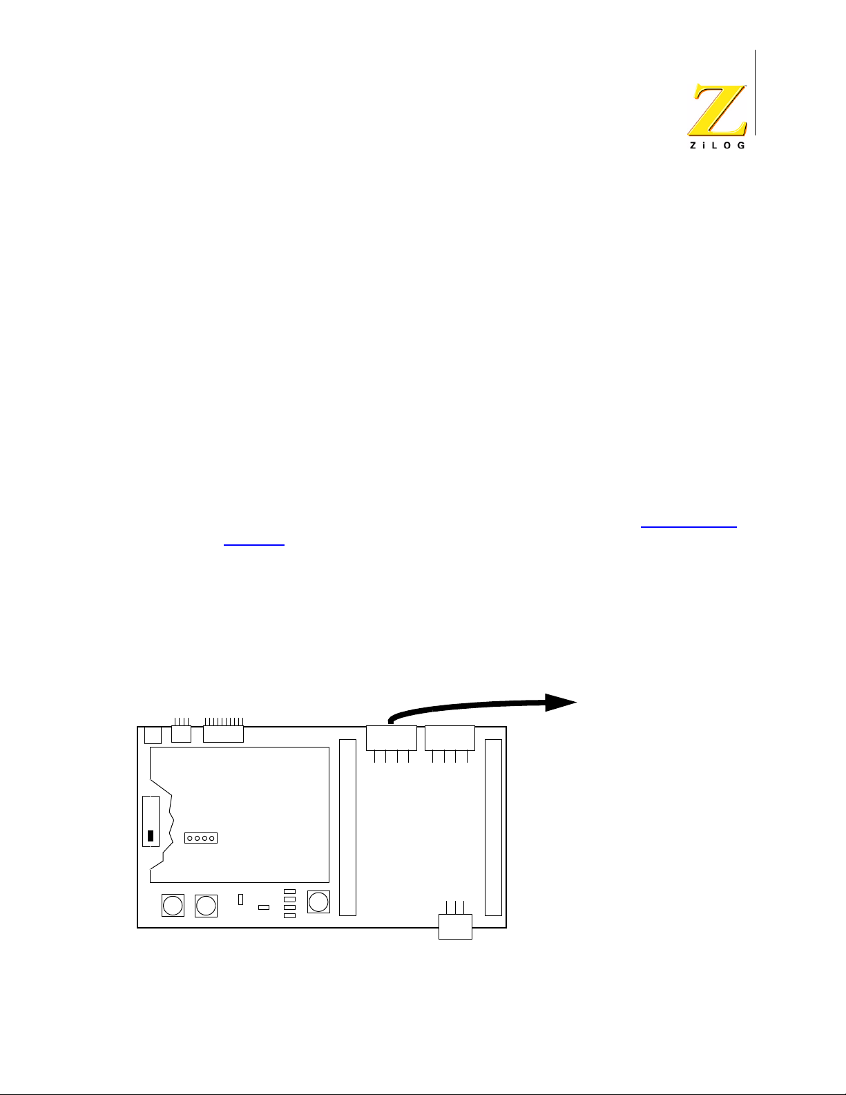
Jumper Locations
Figure 3 illustrates the jumpers on the eZ80® Sales Demonstration Platform.
5VDC
ON
J9
J5
Battery Switch
J2
LCD Display
JP1
eZ80
ZiLOG Development Platforms
®
Sales Demonstration Platform
COM2COM1
JP2
3
SW3
J8
J4
J1
J14
J12
J6
J3
SW1
OFF
I2C Display
Connector
SW2
Figure 3. eZ80® Sales Demonstration Platform Block Diagram
Jumper Settings
J1 CPU Acknowledgement for
Motorola Bus Mode
J3 External Flash Access on
J4 External Flash Boot Block Write
®
eZ80
Module
Access on eZ80
®
Module
J6 IrDA Control IN = IrDA transceiver on the eZ80
IN = enabled
OUT = disabled (default)
IN = Flash access disabled
OUT = Flash access enabled (default)
IN = write enabled
OUT = write disabled (default)
OUT = IrDA transceiver on the eZ80
PB6 is set to 0
ZDI
J7
®
module disabled (default)
®
module enabled when
J12 COM2 (J11) Control IN = Disabled
OUT = Enabled (default)
J14 COM1 (J13) Control IN = Disabled
OUT = Enabled if PB6 set to 1 (default)
User Manual UM015201-0603 Jumper Settings
Page 10
eZ80
eZ80® Sales Demonstration Platform Setup
Overview
A single software project called ez80l92_demo_platform.pro is included on the
®
eZ80
into eZ80L92 Flash memory. Connect the demonstration platform to a PC as
described below and the demo is ready to run.
Instructions for loading the demo project are also included for code download and
debugging demonstrations.
PCB Notes
•
Sales Demonstration Platform CD-ROM. The demo software is preloaded
To use batteries in this demonstration, load four 1.5-Volt batteries into the battery holder and turn on battery switch S1.
ZiLOG Development Platforms
®
Sales Demonstration Platform
4
•
X10 port J10 is not loaded for this release.
•
The LCD module is a Matrix Orbital LCD2041. For further information about
the Matrix Orbital LCD2041 20-column by 4-line display, go to www.matrixor-
bital.com. This LCD display is a 5-volt display with an I2C or RS-232 interface.
This kit uses the I
2
C interface only.
Demonstration Setup Procedure
Ensure that the eZ80® Sales Demonstration Platform is configured and working
properly as described in the eZ80
Guide (QS0024). Then disconnect the ZPAKII from the PC and platform and perform the following procedures. Use Figure 4 as a reference.
5VDC
J9
ON
OFF
Battery Switch
J5
I2C Display
Connector
J2
LCD Display
J8
JP1
®
Sales Demonstration Platform Quick Start
To open COM port
on PC
COM2COM1
JP2
J14
J12
J1
SW1
J6
J3
ZDI
J7
SW2
SW3
J4
Figure 4. eZ80® Sales Demonstration Platform Demo Setup
User Manual UM015201-0603 eZ80® Sales Demonstration Platform Setup
Page 11

eZ80
ZiLOG Development Platforms
®
Sales Demonstration Platform
5
1. Connect a 9-pin serial cable from the PC COM port to connector COM1 on the
2. On the demonstration platform, do one of the following:
Caution:
3. Launch HyperTerminal on the PC by opening the Start menu and selecting
4. In the Connect To dialog, set the Connect Using: drop-down menu to match
®
eZ80
Sales Demonstration Platform.
Connect power to the platform using the AC adapter.
or
Insert four AA batteries into the batter holder on the bottom of the
demonstration platform and turn the BATTERY switch on.
The two LEDs on the demonstration platform blink alternately and the LCD
scrolls feature information for the eZ80L92 chip and eZ80L92 module twice.
When the display completes, the LCD screen displays the time and date.
Proceed with the following instructions to establish communication between
the PC and demonstration platform.
Do not use battery power and AC power at the same time. Doing so will damage
the board.
Programs → Accessories → HyperTerminal, or Programs → Accessories
→ Communications → HyperTerminal, depending on your Windows OS
version.
the COM port to which the eZ80
®
Sales Demonstration Platform is connected.
Click OK.
5. In the resulting COMx Properties dialog, enter the following port settings and
click OK:
Bits per second: 57600
Data bits: 8
Parity: None
Stop bits: 1
Flow control: None
6. Press the RESET button (SW1) on the eZ80
®
Sales Demonstration Platform.
The demonstration platform scrolls through the eZ80L92 and eZ80L92 module
features twice, then displays the time and date.
When the demo completes, HyperTerminal displays the following:
ZiLOG eZ80 Demonstration Platform Program (1.0)
Featuring the eZ80L92
eZ80L92>
User Manual UM015201-0603 eZ80® Sales Demonstration Platform Setup
Page 12

ZiLOG Development Platforms
®
eZ80
Sales Demonstration Platform
7. Press the h key to display the following help text:
eZ80L92> h
ZiLOG eZ80 Demonstration Platform Program (1.0)
Featuring the eZ80L92
C activate/deactivate real time Clock
D set Date
H Help menu
L backLight - On/Off
M display Memory
T set Time
W Write to LCD
2 decrease LED blink speed
3 increase LED blink speed
- decrease LED blink speed
+ increase LED blink speed
? Help menu
6
eZ80L92>
8. Set the date on the demonstration platform. Type D at the prompt and follow
the on-screen instructions. A typical session appears as follows:
eZ80L92> d
Current date is SUNDAY 1-01-2083
Enter new date (dd-mm-yyyy): 20-06-2003
Enter new day-of-the-week: Friday
New date is FRIDAY 20-06-2003
eZ80L92>
9. Set the time on the demonstration platform. Type T at the prompt and follow
the on-screen instructions. A typical session appears as follows:
eZ80L92> t
Current time is 0:41:06
Enter new time (hh:mm:ss): 11:43:00
New time is 11:43:00
eZ80L92>
User Manual UM015201-0603 eZ80® Sales Demonstration Platform Setup
Page 13

You can now run through the available demo project features. A summary of available functions is provided in Table 1.
Table 1. eZ80® Sales Demonstration Platform Demo Features
Feature Description
eZ80
ZiLOG Development Platforms
®
Sales Demonstration Platform
7
Activate/Deactivate Real Time
Clock
Set Date Sets Real Time Clock date.
backlight - On/Off Toggles the demonstration platform LCD screen on and off.
Display Memory Displays the contents of a specified memory segment. Allows
Set Time Sets Real Time Clock time.
Write to LCD Allows the user to write up to four lines of 20 characters each to
Decrease LED blink speed Slows the blink rate of the two LEDs on the demonstration plat-
Increase LED blink speed Increases the blink rate of the two LEDs on the demonstration
Demonstrates Real Time Clock control. Deactivating the Real
Time Clock removes the date and time display from the demonstration platform LCD screen.
the user the specify a starting address and number of bytes to
display.
the sales demonstration platform LCD display.
form by 16ms each time the user presses the 2 or - key. Pressing switch SW2 on the demonstration platform has the same
effect.
platform by 16ms each time the user presses the 3 or + key.
Pressing switch SW3 on the demonstration platform has the
same effect.
Using ZDSII to Download and Run ez80l92_demo_platform.pro
Use the following instructions to demonstrate code download and running the
demo project in the ZDSII debugger.
1. Connect the ZPAK II to the eZ80
®
in the eZ80
Sales Demonstration Platform Quick Start Guide (QS0024).
2. Launch ZDS II. (Start menu → Programs → ZiLOG ZDS II–eZ80_<Version>
→ ZDS II–eZ80_<Version>).
3. In ZDS II, select File → Open Project, and navigate to the following file path:
c:\Program Files\ZiLOG\ZDSII_ez80_<version>\applications\eZ80L92_Demo_Platform\src
4. Select the ez80l92_demo_platform.pro project and click Open. A list of
source files appears in the Workspace panel.
5. Select Project → Settings.
User Manual UM015201-0603 eZ80® Sales Demonstration Platform Setup
®
Sales Demonstration Platform as described
Page 14

ZiLOG Development Platforms
®
eZ80
Sales Demonstration Platform
6. The Settings dialog appears. Select the Debugger tab. In the Debugger tab,
click on the Configure ZPAK II button.
7. The Configure ZPAK II dialog box appears. In the IP Address field, a default IP
address, 192.168.1.50, is displayed and highlighted. Enter the ZPAK II IP
address you configured during hardware install. (Either the default of
192.168.1.50 or the IP address to which you set the ZPAK II.) Leave the other
settings as they are.
8. Click OK in the Configure ZPAK II dialog, and then click OK in the Project Settings dialog.
9. Select Build → Rebuild All. Wait for the build to complete (Status panel indicates Build Complete).
10. Download the demo into the eZ80® Sales Demonstration Platform by selecting Build → Debug → Reset.
8
11. To run the demo, select Build → Debug → Go.
12. When the demo software runs, the demonstration platform LCD screen displays ez80L92 and eZ80L92 module features, then displays the time and
date.
13. Select Build → Debug → Stop Debugging to stop the demo.
Peripheral Bus Connector
Figure 5 illustrates the 60-pin peripheral bus connector, JP1. Table 2 describes
the pins and their functions. (Pin 50 on the eZ80L92 module connectors line up
with pin 60 on the eZ80
connector is keyed to help orient the board.) Refer to the module product specification on the demonstration platform CD for pin functions and locations.
®
Sales Demonstration Platform board connectors. The
User Manual UM015201-0603 Peripheral Bus Connector
Page 15

eZ80
J
ZiLOG Development Platforms
®
Sales Demonstration Platform
9
2
4
6
8
10
12
14
16
18
20
22
24
26
28
30
32
34
36
38
40
42
44
46
48
50
52
54
56
58
60
VCC_33V
A0
A3
VCC_33V
A7
A9
A14
A16
GND
A1
A12
A20
A17
-DIS_FLASH
VCC_33V
A23
-CS1
D0
D2
D4
GND
D6
-IOREQ
-RD
-INSTRD
-BUSREQ
-TRSTN
-F91_WE
GND
-CS2
GND
A6
A10
GND
A8
A13
A15
A18
A19
A2
A11
A4
A5
A21
A22
-CS0
D1
D3
D5
D7
-MREQ
-WR
-BUSACK
1
3
5
7
9
11
13
15
17
19
21
23
25
27
JP1
29
31
33
35
37
39
41
43
45
47
49
51
53
55
57
59
Figure 5. eZ80® Sales Demonstration Platform Peripheral Bus Connector Pin Configuration
Table 2. Peripheral Bus Connector Pin Identification (see Figure 5 for Pin #s)
Signal Direction
(with respect to
Pull
Function
A0 - A23 n/a Bidirectional 24-bit address bus
Up/Down*
the Platform
board) Description
D0 - D7 n/a Bidirectional 8-bit data bus
TRSTN OUT Reset for On-Chip Instrumentation (OCI).
F91_WE OUT Low enables write to on-chip Flash memory.
If this pin is unconnected, on-chip Flash
memory is write-protected.
DIS_FLASH OUT External Flash Memory enable input.
CS0 - CS2 n/a IN Chip Selects for on-board or external devices
MREQ Bidirectional Bus Cycle Memory indication.
Notes: *External capacitive loads on RD, WR, IOREQ, MREQ, D0–D7 and A0–A23 must be below 10pF to
satisfy timing requirements for the eZ80® CPU. All unused inputs must be pulled to either VDD or
GND, depending on their inactive levels to reduce power consumption and to reduce noise sensitivity.
To prevent EMI, the EZ80CLK output can be deactivated by software in the eZ80F92 Peripheral
Power-Down Register. All inputs are CMOS level 3.3V (5V tolerant), except where otherwise noted.
User Manual UM015201-0603 Peripheral Bus Connector
Page 16

ZiLOG Development Platforms
®
eZ80
Table 2. Peripheral Bus Connector Pin Identification (see Figure 5 for Pin #s)
Signal Direction
(with respect to
Pull
Function
Up/Down*
IOREQ Bidirectional Bus Cycle I/O indication.
RD Bidirectional Bus Cycle read indication.
WR Bidirectional Bus Cycle write indication.
INSTRD n/a IN Bus Cycle Instruction read indication
BUSACK IN Bus Acknowledge output
BUSREQ Pull-Up 10k OUT Bus Request input
the Platform
board) Description
Sales Demonstration Platform
10
V
CC
GND n/a n/a V
Notes: *External capacitive loads on RD, WR, IOREQ, MREQ, D0–D7 and A0–A23 must be below 10pF to
satisfy timing requirements for the eZ80
GND, depending on their inactive levels to reduce power consumption and to reduce noise sensitivity.
To prevent EMI, the EZ80CLK output can be deactivated by software in the eZ80F92 Peripheral
Power-Down Register. All inputs are CMOS level 3.3V (5V tolerant), except where otherwise noted.
n/a n/a 3.3 V Supply Input Pin
/Ground (0V)
SS
®
CPU. All unused inputs must be pulled to either VDD or
User Manual UM015201-0603 Peripheral Bus Connector
Page 17

I/O Connector
PB0
-HALT_SLP
PA1
PD7
EZ80CLK
VCC_33V
PC1
PB1
PB3
GND
PD4
PA6
PD2
GND
PD0
PC6
PC0
-CS3
TRIGOUT
TMS
PA4
PD3
PA7
PC7
PB4
TDO TDI
GND
-WAIT
PA2
PC4
VCC_33V
PA5
RTC_VDD
PC5
GND
-NMI
PC3
GND
PC2
PA3
IICSDA
PA0
PD5
IICSCL
VCC_33V
PD6
PD1
PB2
TCK
-RESET
-FLASHWE
PB7
GND
PB5
-DIS_IRDA
2
4
6
8
10
12
14
16
18
20
22
24
26
28
30
32
34
36
38
40
42
44
46
48
50
52
54
56
58
60
1
3
5
7
9
11
13
15
17
19
21
23
25
27
29
31
33
35
37
39
41
43
45
47
49
51
53
55
57
59
Figure 6 illustrates the 60-pin I/O Connector, JP2. Table 3 describes the pins and
their functions. (Pin 50 on the eZ80L92 and eZ80F92 module connectors line up
with pin 60 on the eZ80
ZiLOG Development Platforms
®
eZ80
®
Sales Demonstration Platform board connectors.)
JP2
Sales Demonstration Platform
11
User Manual UM015201-0603 I/O Connector
Figure 6. eZ80® Sales Demonstration Platform I/O Connector Pin Configuration
Function
PA0 - PA7 Bidirectional Not used for eZ80L92 and eZ80F92 modules.
PB0 - PB7 Bidirectional These pins can be used for general-purpose I/O.
Pull
Up/Down
Table 3. I/O Connector Pin Identification
Signal
Direction Description
They can be individually programmed as input or out-
put and can also be used individually as interrupt
inputs. Each Port B pin, when programmed as output,
can be selected to be an open-drain or open-source
output.
Page 18

ZiLOG Development Platforms
®
eZ80
Table 3. I/O Connector Pin Identification (Continued)
Sales Demonstration Platform
12
Function
Pull
Up/Down
Signal
Direction Description
PC0 - PC7 Bidirectional These pins can be used for general-purpose I/O.
They can be individually programmed as input or out-
put and can also be used individually as interrupt
inputs. Each Port C pin, when programmed as output,
can be selected to be an open-drain or open-source
output. Port C is multiplexed with one UART.
PD0 - PD7 Bidirectional These pins can be used for general-purpose I/O.
They can be individually programmed as input or out-
put and can also be used individually as interrupt
inputs. Each Port D pin, when programmed as output,
can be selected to be an open-drain or open-source
output. Port D is multiplexed with one UART.
TDO IN JTAG Data Output pin.
TDI OUT JTAG Data Input pin.
ZDA Bidirectional ZDI Data I/O. (Shared with TDI pin.)
TRIGOUT IN Active High trigger event indicator.
TCK PU 10 K OUT JTAG Input. High on reset enables ZDI mode; Low on
reset enables OCI debug.
ZCL OUT ZDI Clock Input. High on reset enables ZDI mode;
Low on reset enables OCI debug. (Shared with TCK
pin.)
TMS PU 10K OUT JTAG Test Mode Select Input.
RTC_V
DD
n/a RTC supply from eZ80® module battery.
CLKOUT IN 20MHz synchronous CPU clock output from product
module.
IICSCL PU 4k Bidirectional I
IICSDA PU 4k Bidirectional I
F
lashWE PU 10K OUT When low, enables write operation on boot block of
2
C Bus Clock.
2
C Data Clock.
external Flash memory on the module.
CS3 IN Chip select for on-board or external devices
DIS_IRDA
PU 10K OUT Low disables module on-board IRDA transceiver to
use PD0/PD1 UART pins externally.
RESET
PU 2k Schmitt Trigger
Reset Output from module or push-button reset.
OUT, Active
Low
User Manual UM015201-0603 I/O Connector
Page 19

ZiLOG Development Platforms
®
eZ80
Table 3. I/O Connector Pin Identification (Continued)
Sales Demonstration Platform
13
Function
Pull
Up/Down
Signal
Direction Description
WAIT PU 2k OUT Driving the WAIT pin Low forces the eZ80® CPU to
provide additional clock cycles for an external periph-
eral or external memory to complete its READ or
WRITE operation.
HALT_SLP
IN, Active Low A Low on this pin indicates that the eZ80® CPU
enters either HALT or SLEEP mode because of exe-
cution of either a HALT or SLP instruction.
NMI
PU 10K Schmitt Trigger
OUT, Active
Low
The NMI input is a higher priority input than the
maskable interrupts. It is always recognized at the
end of an instruction, regardless of the state of the
interrupt enable control bits. This input includes a
Schmitt trigger to allow RC rise times. This external
NMI
signal is combined with an internal NMI signal
generated from the WDT block before being con-
V
CC
n/a 3.3V Supply Input Pin.
GND n/a V
nected to the NMI
/Ground (0V)
SS
input of the eZ80® CPU.
User Manual UM015201-0603 I/O Connector
Page 20

Sales Demonstration Platform
ZiLOG Development Platforms
®
eZ80
14
DB7
DB3
DB5
A0
-RD
DB1
VCC_5V
-RESET
123
4
J5
OFF BOARD
I2C
123
4
J8
DISPLAY I2C
J1
Motorola Mode
-DACK_EN
2
1
-WAIT
-CS2
C17
VCC_5V
J2
12
34
56
78
-WR
DB0
DB2
GND
DB4
DB5
DB2
DB3
DB0
GND
20
U1
DB1
7
6
5
4
3
2
A0A1A2A3A4A5A6
VCCGND
B0B1B2B3B4B5B6
13
14
15
16
17
18
0.1uF
910
11 12
DB4
DB6
8
12
HEADER 10X2
15 16
17 18
19 20
13 14
IICSDA
VCC_5V
GND
IICSCL
R18
R17
4.7K
DB6
-CS2
OFF BOARD DATA BUS
DB7
-WR
-CS2
1
19
9
A7
B7
11
GND
G
DIR
10
74ACT245
4.7K
VCC_5V
IICSDA
IICSCL
GND
Put R17 and R18 in only
when Encore! F08 Board
is used
Sales Demonstration Platform.
®
D0D1D2D3D4D5D6
PB6
R30
10K
VCC_33V
GND
PB2
PB4
PB0
PA0
PA2
PA4
PA6
6
4
2
JP2
5
3
1
connector 2
PA3
PA5
PA7
PC7
20
18
16
14
12
10
8
9
7
19
17
15
13
11
PB5
PB7
PA1
PB1
GND
PB3
VCC_33V
R2
680
R3
D7
74LV05
5
U7C
J6
2
1
GND
DIS_IrDA
VCC_33V
SW3
SW2
R7
R6
10K
R5
10K
PB3
SW PUSHBUTTON
SW PUSHBUTTON
R8
100
PB4
Sales Demonstration Platform Schematic
®
100
Figure 1. eZ80
6
R32
10K
VCC_33V
-DIS_IRDA
RED
GND
EZ80CLK
TRIGOUT
TMS
PD0
44
42
40
38
36
43
41
39
37
35
TDO TDI
PD1
TCK
RTC_VDD
GND
1
1
J4
46
45
IICSCL
-NMI-BUSACK
-WAIT
GND
60
58
56
54
52
50
48
HEADER 30x2/SM
59
57
55
53
51
49
47
IICSDA
VCC_33V
-CS3
-RESET
-FLASHWE
-HALT_SLP
VCC_33V
RES
2
1
FL_WE
GND
PD2
PD4
PC3
PC5
PC1
PD7
34
32
30
28
26
24
22
33
31
29
27
25
23
21
PD6
PD5
PC2
PC4
PD3
PC6
PC0
D2
YEL
2
680
D1
2
Figures 1 and 2 provide schematics of the eZ80
JP1
connector 1
Schematic
J3
A1
A12
GND
A7
A9
A14
A16
A3
A0
VCC_33V
VCC_33V
30
28
26
24
22
20
18
16
14
10
12
8
6
2
4
9
7
3
5
1
13
11
A6
A10
GND
-TRSTN
-F91_WE
272931
25
21
23
17
19
15
A2
A18
GND
A11
A15
A19
A8
A13
DIS_FL
2
1
VCC_33V
A20
D0
D2
A17
-CS1
A23
-DIS_FLASH
46
44
42
40
38
36
32
34
45
41
43
39
35
37
33
A4
D1
A5
A21
-CS0
A22
-CS2
VCC_33V
10K
R4
-BUSREQ
-INSTRD
D6
-IOREQ
-RD
D4
GND
58
60
56
54
50
52
48
HEADER 30x2/SM
59
535557
51
49
47
D3
-WR
D5
D7
-MREQ
GND
J7
ZDI
INTERFACE
TCK
12
34
56
Header 3x2
GND TDI
VCC_33V
VCC_5V
GND
VCC_33V
VCC_5V
GND
VCC_33V
User Manual UM015201-0603 Schematic
Page 21

15
X10
BATTERY ON
3.3 OK
RS232 - 1
RS232 - 2
RS232-1 DIS
RS232-2 DIS
POWER SUPPLY
<Doc>
eZ80 Demo Platform. Power supply & Communication
B
2Tuesday April 15 2003
Title
Size Document Number
Date: Sheet
of
RTS1RxD1
RTS0
GND
CTS0
GND
TxD0
RxD0
TxD1 CTS1
GND
RTS1
RxD1
PC3
PC0
CTS1
TxD1
5V
VCC_5V
PC1
VCC_33V
3.3V
VCC_33V
PC2
GND
VCC_33V
TxD0
CTS0
RxD0
VCC_33V
GND
GND
RTS0
VCC_33V
GND
GND
GND
GND
GND
VCC_33V
GND
VCC_33V
VCC_33V
VCC_33V
VCC_33V
VCC_33V
VCC_5V
PC0
PC2
PC1
PC3
PD2
PD0
PD1
PD3
GND
PB0
PB1
PB2
PB6
J10
12345
6
C5
0.1uF
J12
1
2
J14
1
2
R1
10K
C9
0.1uF
U4
TPS7250
1
2
3
4
5
6
7
8
SENSE
PG
GND
EN
IN
IN
OUT
OUT
U7B
74LV05
34
U7F
74LV05
1312
C12
0.1uF
C13
0.1uF
J13
CON10A
13579
246
8
10
R20
10K
D3
GREEN
21
U7D
74LV05
98
C7
0.1uF
R11
10K
C11
0.1uF
R33
10K
R29
10K
U3
LT1086-3.3/TO220
1
3 2
GND
VIN VOUT
BT1
BATTERY
R21
10K
+
C6
10uF
R12
10K
U7A
74LV05
1 2
147
R9
680
+
C2
22uF
C8
0.1uF
R22
10K
C14
0.1uF
U5 MAX3222
1
245
6
131215
10
3
7
17816
9
20
1918
11
14
EN
C1+
C1-
C2+
C2-
T1IN
T2IN
R1OUT
R2OUT
V+
V-
T1OUT
T2OUT
R1IN
R2IN
SHDN
VCCGND
NC
NC
C16
0.1uF
J9
PWR JACK
231
J11
CON10A
13579
246
8
10
R13
10K
R31
10K
+
C3
22/6.3
C1
0.1
S1
U7E
74LV05
1110
C4
0.1
C15
0.1uF
F1
RXE160
C10
0.1uF
R10
200K
R28
10K
U6
MAX3222
1
245
6
131215
10
3
7
17816
9
20
1918
11
14
EN
C1+
C1-
C2+
C2-
T1IN
T2IN
R1OUT
R2OUT
V+
V-
T1OUT
T2OUT
R1IN
R2IN
SHDN
VCCGND
NC
NC
Sales Demonstration Platform
ZiLOG Development Platforms
®
eZ80
Sales Demonstration Platform
®
Figure 2. eZ80
User Manual UM015201-0603 Schematic
 Loading...