

ZHIXUAN ZXXS133-L02 Specification

Global LCD Panel Exchange Center
Global LCD Panel Exchange Center
www.panelook.com
www.panelook.com
Issued Date:
Model No.: ZXXS133-L02
Aug. 26, 2008
TFT LCD
Approval Specification
MODEL NO.:ZXXS133-L02
ustomer:
C
Approved
by:
Appr
oval
Note:
ʳʳʳ ʳʳ
ʳ
ʳʳ
ʳ
1 / 27
One step solution for LCD / PDP / OLED panel application: Datasheet, inventory and accessory!
ersion 2.2
V
www.panelook.com
www.panelook.com
Global LCD Panel Exchange Center
Global LCD Panel Exchange Center
www.panelook.com
www.panelook.com
Issued Date:
Model No.:ZXXS133-L02
Aug. 26, 2008
- CONTENTS -
REVISI
1. GENERAL
1.2 FEATURES
1.3 APPLICATION
1.4 GENERAL SPECIFICATIONS
1.5 MECHANICAL SPECIFICATIONS
2.
2.2 ELECTRICAL ABSOLUTE RATINGS
2.2.1 TFT LCD MODULE
2.2.2 BACKLIGHT UNIT
3. ELECTRI
ON HISTORY
DESCRIPTION
1.1 OVER
VIEW
ABSOLUTE MAXIMUM RATINGS
2.1 ABSOLUTE RATINGS OF ENVIRONMENT
CAL CHARACTERISTICS
3.1 TFT
3.2 BACKLIGHT UNIT
LCD MODULE
Appr
------------------------------------------------------- 3
------------------------------------------------------- 4
-----------------------------------------------------
--
-----------------------------------------------------
--
oval
5
7
4. BLOCK DIAGRAM --
4.1 TFT LCD MODULE
4.2 BACKLIGHT UNIT
5. INPUT TERMINAL PIN ASSIGNMENT --
TFT LCD MODULE
5.1
5.2 BACKLIGHT UNIT
5.3 TIMING DIAGRAM OF LVDS INPUT SIGNAL
5.4 COLOR DATA INPUT ASSIGNMENT
5.5 EDID DATA STRUCTURE
-----------------------------------------------------
-----------------------------------------------------
11
12
6. INTERFACE TIMING ------------------------------------------------------- 16
6.1 INP
6.2 POWER ON/OFF SEQUENCE
7. OPTICAL CHARACTERISTICS
7.1 TEST CONDITIONS
7.2 OPTICAL SPECIFICATIONS
8. PRECAUTIONS
8.1
8.2 STORAGE PRECAUTIONS
8.3 OPERATION PRECAUTIONS
9. P
9.1 CA
9.2 PALLET
UT SIGNAL TIMING SPECIFICATIONS
HANDLING PRECAUTIONS
ACKING
RTON
-----------------------------------------------------
--
--
-----------------------------------------------------
-----------------------------------------------------
--
18
22
23
10. DEFINITION OF LABELS
10.1 CMO MODULE
10.2 CMO CARTON LABE
10.3 CUSTOMER CARTON LABEL
10.4 CUSTOMER PALLET LABEL
LABEL
--
-----------------------------------------------------
2 / 27
One step solution for LCD / PDP / OLED panel application: Datasheet, inventory and accessory!
25
ersion 2.2
V
www.panelook.com
www.panelook.com
Global LCD Panel Exchange Center
Global LCD Panel Exchange Center
www.panelook.com
www.panelook.com
Issued Date:
Model No.: ZXXS133-L02
Aug. 26, 2008
V
ersion Date
2.0
2.1
2.1
2.2
2007.08.16
2008.04.28
2008.04.28
2008.08.26
Page
(New)
All
5
17
19
21
Appr
REVISION HIST
Section Description
All
2.1
6.2
7.2
8.1
Approval
Vibration (Non-operation) test condition from
5Hz, 100Hz, 200Hz, 1.47Grms X, Y, Z three axes (30min /axis) to
1.5G, 10~300Hz, 10min/cycle,3 cycles each X,Y,Z
Contrast Ratio Modified, Typ. 500 -> 800
Min. 350 -> 550
Optical SpecificationΚModify note (5) measurement setup figure.
Add precaution of “Image sticking” in section 8.1 Assembly and
handling precautions
(11) Do not keep same pattern in a long period of time. It may cause
image sticking on LCD
specification was first issued.
ORY
oval
3 / 27
One step solution for LCD / PDP / OLED panel application: Datasheet, inventory and accessory!
ersion 2.2
V
www.panelook.com
www.panelook.com

Global LCD Panel Exchange Center
Global LCD Panel Exchange Center
www.panelook.com
www.panelook.com
Issued Date:
Model No.: ZXXS133-L02
Aug. 26, 2008
Appr
1. GENERAL DESCRIPTION
1.1 OVERVIEW
ZXXS133 - L02 is a 13.3” TFT Liquid Crystal Display Rohs module and 20 pins LVDS interface. This module
supports 1280 x 800 WXGA mode and can display 262,144 colors. The optimum viewing angle is at 6
o’clock direction. The inverter module for Backlight is not built in.
1.2 FEA
1.3 APPLICATION
TURES
- WXGA (1280 x 800 pixels) resolution
- DE only mode
- 3.3V LVDS (Low Voltage Differential Signaling) interface with 1 pixel/clock
- RoHs compliance
TFT LCD Panel
-
oval
1.4 GENERAL SPECIFICATI0NS
Item Specification Unit Note
Active
Area 286.08 (H) x 178.8 (V) mm
Bezel O
Driver Element
Pixel Number
Pixel Pitch
Pixel
Display Col
T
Surface
1.5 MECHANICAL
Module Size
I/F
Note (1)
Note (2) Connector mounting position
pening Area 289.1 (H) x 181.8 (V) mm
a-si TFT active matrix - -
1280 x R.G.B. x 800 pixel -
0.2235 (H) x 0.2235 (V) mm -
Arrangement RGB vertical stripe - -
ors 262,144 color -
ransmissive Mode Normally white - -
Treatment AG , 25%Haze - -
SPECIFICATIONS
Item Min.
Horizont
V
ertical(V) 194.5 195 195.5 mm
Depth(D) - 7.7 8.0 mm
eight - 450 465 g -
W
connector mounting position The mounting inclination of the connector makes the screen
Please refer to the attached drawings for more information of front and back outline dimensions.
al(H) 298.5 299 299.5 mm
center within ±0.5mm as the horizontal.
Typ. Max. Unit Note
(1)
(1)
(2)
+/- 0.5mm
4 / 27
One step solution for LCD / PDP / OLED panel application: Datasheet, inventory and accessory!
ersion 2.2
V
www.panelook.com
www.panelook.com
Global LCD Panel Exchange Center
Global LCD Panel Exchange Center
www.panelook.com
www.panelook.com
Issued Date:
Model No.: ZXXS133-L02
Aug. 26, 2008
2. ABSOLUTE MAXIMUM RATINGS
2.1 ABSOLUTE RATINGS OF ENVIRONMENT
V
Item Symbol
Operating Am
torage Temperature T
S
est Item Test Condition Note
T
High Temperature Storage Test 80ºC, 240 hours
Temperature Storage Test -30ºC, 240 hours
Low
Thermal Shock Storage Test
Temperature Operation Test 70ºC, 240 hours
High
Low Temperature Operation Test -30ºC, 240 hours
High
Temperature & High Humidity
Operation Test
Heat Cy
est (Operation)
ESD T
Shock (Non-Operating)
Vibration (Non-Operating) 1.5G,10~300Hz,10min/cycle,3 cycles each X,Y,Z (2)(3)
bient Temperature T
cle Operation Test
-30ºC, 0.5hourЧШ80к, 0.5hour; 100cycles, 1hour/cycle
60ºC, 90%RH, 240hours
-20ºC, 1hourЧШ70ºC, 1hour; 50cycles, 4hour/cycle
150pF, 330Ө, 1sec/cycle
Condition 1 : panel contact, 8KV
Condition 2 : panel non-contact 15KV
200G, 2ms, half sine wave, 1 time for ± X, ± Y, ± Z. (2)(3)
OP
-30
ST
Min. Max.
-30 +70 ºC (0), (1), (2)
alue
Unit Note
+80 ºC (0), (1)
Appr
(1) (2)
(2)
oval
Note (1)
(a) 90 %RH Max. (Ta Љ 40 ºC).
(b) Wet-bulb temperature should be 39 ºC Max. (Ta > 40 ºC).
(c) No condensation.
Note (2) No display malfunctions.
Note (3) At testing Vibration and Shock, the fixture in holding the module has to be hard and rigid enough
Note (4) Temperature of panel display surface area should be 80 ºC Max.
Note (5) In the standard conditions, there is no function failure issue occurred. All the cosmetic specification
is judged before the reliability test
Temperature and relative humidity range is shown in the figure below.
so that the module would not be twisted or bent by the fixture.
5 / 27
One step solution for LCD / PDP / OLED panel application: Datasheet, inventory and accessory!
ersion 2.2
V
www.panelook.com
www.panelook.com
Global LCD Panel Exchange Center
Global LCD Panel Exchange Center
www.panelook.com
www.panelook.com
Issued Date:
Model No.: ZXXS133-L02
Aug. 26, 2008
Appr
2.2 ELECT
2.2.1 TFT LCD MODULE
Powe
Logi
2.2.2 BACKLIGHT UNIT
Lamp Voltage VL 2.5k V
Lamp Current
Lamp F
Note (1) Permanent damage to the device may occur if maximum values are exceeded. Function operation
Note (2) Specified values are for lamp (Refer to 3.2 for further information).
RICAL ABSOLUTE RATINGS
V
Item Symbol
r Supply Voltage V
c Input Voltage V
Item Symbol
requency F
should be restricted to the conditions described under Normal Operating Conditions.
-0.3
CC
-0.3
IN
I
2.0
L
50
L
Min. Max.
Min. Max.
alue
V
alue
Unit Note
+4.0 V
V
+0.3 V
CC
Unit Note
(1), (2), IL = 6.5 mA
RM
S
7.0 mA
80 KHz
RMS
(1)
(1), (2)
oval
6 / 27
One step solution for LCD / PDP / OLED panel application: Datasheet, inventory and accessory!
ersion 2.2
V
www.panelook.com
www.panelook.com
Global LCD Panel Exchange Center
Global LCD Panel Exchange Center
www.panelook.com
www.panelook.com
Issued Date:
Aug. 26, 2008
Model No.:ZXXS133-L02
Appr
3. ELECTRICAL CHARACTERISTICS
3.1 TFT LCD MODULE
Param
eter Symbol
Powe
r Supply Voltage Vcc 3.0 3.3 3.6 V -
ssive Ripple Voltage V
Permi
Rush Current I
Initial S
Power Supply Current
L
L
LVDS Common Mode Voltage VCM 1.125 1.375 V (4)
L
T
Note (1)
Note (2) I
I
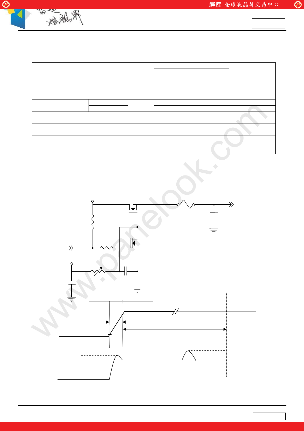
Measurement Conditions: Shown as the following figure. Test pattern: black
tage Current I
White
Black
VDS Differential Input High Threshold V
VDS Differential Input Low Threshold V
VDS Differential Input Voltage |V
erminating Resistor R
The ambient temperature is Ta = 25 ± 2 ºC.
: the maximum current when VCC i
RUSH
:
the maximum current of the first 100ms after power-on
IS
+3.3
V
R1
47K
T
T
1 2SK1475
Q
Ta = 25 ± 2 ºC
Value
Min. Typ. Max.
RP
1.5 A (2)
RUSH
IS
Icc
H(LVDS)
L(LVDS)
| 100
ID
T
50 mV -
1.0 A (2)
330 370 mA (3)a
450 490 mA (3)b
-10
0 mV
+100 mV
600 mV (4)
100 Ohm
Unit Note
V
V
s rising
c
Vc
(LCD Module Input)
FUS
E
C3
1uF
(4),
=1.2V
CM
(4)
=1.2V
CM
oval
(Hi
gh to Low)
(Control Signal)
SW
+12
0V
I
V
C1
1uF
RUSH
Q2
2SK
1470
C2
VR1
R2
1K
47K
0.01uF
Vcc rising time is 470us
0.9Vcc
s
470u
0.1Vcc
+3.3V
100m
VCC
s
I
IS
ICC
7 / 27
One step solution for LCD / PDP / OLED panel application: Datasheet, inventory and accessory!
ersion 2.2
V
www.panelook.com
www.panelook.com

|
|
|
|
Global LCD Panel Exchange Center
Global LCD Panel Exchange Center
www.panelook.com
www.panelook.com
Issued Date:
Model No.: ZXXS133-L02
Aug. 26, 2008
(3) The specified power supply current is under the conditions at Vcc = 3.3 V, Ta = 25 ± 2 ºC, f
Note
Hz, whereas
a. White Pattern
a power dissipation check pattern below is displayed.
b. Black Pattern
Active Area
Active Area
Appr
= 60
v
oval
Note (4) The parameters of LVDS signals are defined as the following figures.
CM
V
Single Ended
0V
V
Differentia
l
0V
V
VID
V
ID
8 / 27
One step solution for LCD / PDP / OLED panel application: Datasheet, inventory and accessory!
ersion 2.2
V
www.panelook.com
www.panelook.com
Global LCD Panel Exchange Center
Global LCD Panel Exchange Center
www.panelook.com
www.panelook.com
Issued Date:
Aug. 26, 2008
Model No.: ZXXS133-L02
3.2
BACKLIGHT UNIT
Parameter Symbol
Lamp Input V
oltage V
531
L
Min. Typ. Max.
Value
590 649 V
Lamp Current IL 2.0 6.5 7.0 mA
(25к)
Turn On Voltage V
Lamp
rating Frequency F
Ope
Lamp Life
Powe
Note (1)
Time L
r Consumption P
Lamp current is measured by utilizing a high frequency current meter as shown below:
LCD
Module
S
50
L
5000
BL
L
HV (Pin
-- --
0 -- -- Hrs (5)
k)
LV (White)
-- --
-- 80 KHz (3)
12 -- W (4), I
1
2
A
Cu
rrent Meter
1080
1290
(0к)
Inverter
Appr
Ta = 25 ± 2 ºC
oval
Unit Note
I
RMS
RMS
V
(2)
RMS
(2)
V
RMS
= 6.5 mA
L
(1)
= 6.5 mA
L
Note (2) The voltage that must be larger than Vs should be applied to the lamp for more than 1 second
after startup. Otherwise, the lamp may not be turned on normally.
Note (3) The lamp frequency may produce interference with horizontal synchronous frequency from the
display, and this may cause line flow on the display. In order to avoid interference, the lamp
frequency should be detached from the horizontal synchronous frequency and its harmonics as far
as possible.
Note (4) P
Note
= I
L
LVL
(5) The lifetime of lamp can be defined as the time in which it continues to operate under the condition
Ta = 25 2
o
C and IL = 6.5 mArms until
one of the following events occurs:
(a) When the brightness becomes or lower than 50% of its original value.
(b) When the effective ignition length becomes Љ 80% of its original value. (The effective ignition
length is a scope that luminance is over 70% of that at the center point.)
Note (6) The waveform of the voltage output of inverter must be area-symmetric and the design of the
inverter must have specifications for the modularized lamp. The performance of the Backlight,
such as lifetime or brightness, is greatly influenced by the characteristics of the DC-AC inverter for
the lamp. All the parameters of an inverter should be carefully designed to avoid producing too
much current leakage from high voltage output of the inverter. When designing or ordering the
inverter please make sure that a poor lighting caused by the mismatch of the Backlight and the
inverter (miss-lighting, flicker, etc.) never occurs. If the above situation is confirmed, the module
should be operated in the same manners when it is installed in your instrument.
The output of the inverter must have symmetrical (negative and positive) voltage waveform and
symmetrical current waveform.(Unsymmetrical ratio is less than 10%) Please do not use the inverter
9 / 27
One step solution for LCD / PDP / OLED panel application: Datasheet, inventory and accessory!
One step solution for LCD / PDP / OLED panel application: Datasheet, inventory and accessory!
ersion 2.2
V
www.panelook.com
 Loading...