

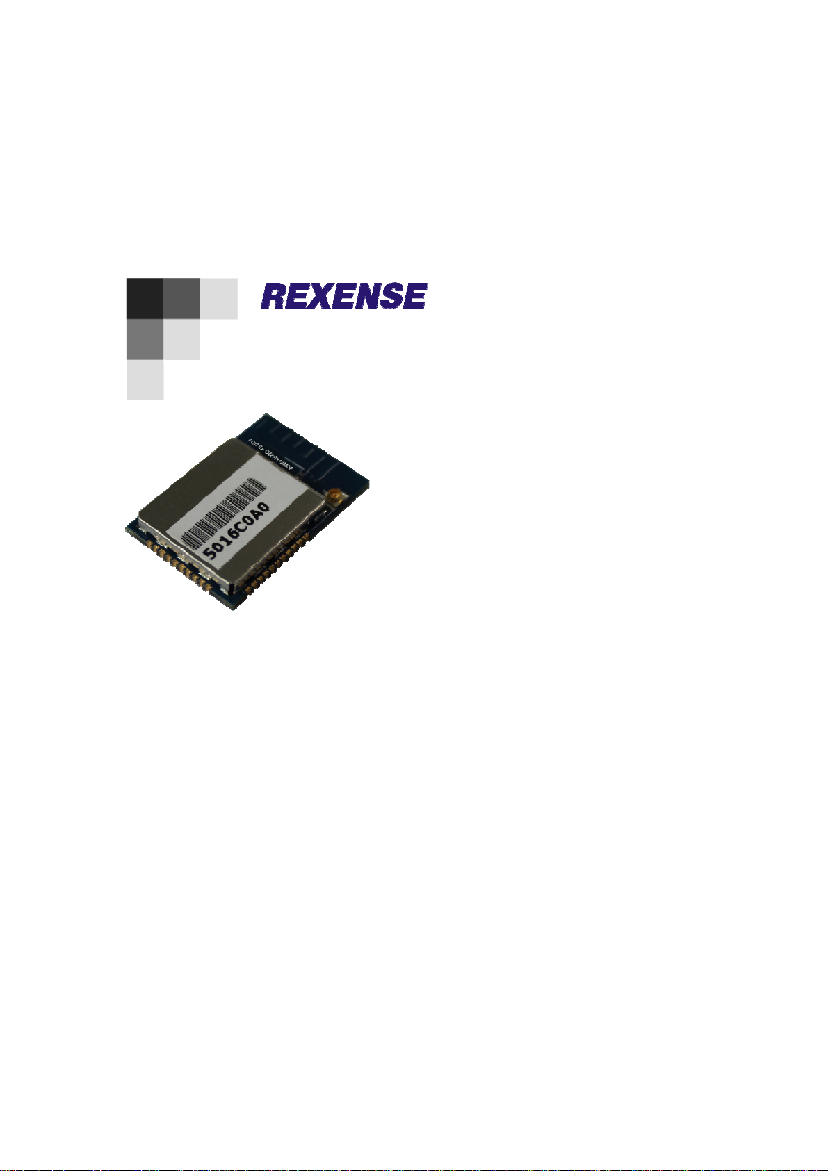
802.15.4/ ZigBee Module Datasheet
REX3SP
ZHEJIANG REXENSE TECHNOLOGY CO., LTD.

COPYRIGHT INFO
The information contained in this document is the proprietary information of Zhejiang
Rexense Technology Co., Ltd. (hereinafter referred as Rexense). The contents are
confidential and any disclosure to persons other than the officers, employees, agents or
subcontractors of the owner or licensee of this document, without the prior written consent
of Rexense, is strictly prohibited.
Further, no portion of this document may be reproduced, stored in a retrieval system, or
transmitted in any form or by any means, electronic or mechanical, including photocopying
and recording, without the prior written consent of Rexense, the copyright holder.
Rexense publishes this document without making any warranty as to the content contained
herein. Further Rexense reserves the right to make modifications, additions and deletions
to this document due to typographical errors, inaccurate information, or improvements to
products mentioned in the document at any time and without notice. Such changes will,
nevertheless be incorporated into new editions of this document
VERSION HISTORY
V1.0.0 2011/06/04 1st issue of preliminary document
V1.0.1 2012/08/30 Add the section of
Agency Certifications
www.rexense.com
1

Table of Contents
1. Introduction................................................................................................................................3
1.1 Summary...........................................................................................................................3
1.2 Applications.......................................................................................................................3
1.3 Key Features.....................................................................................................................3
1.4 Benefits.............................................................................................................................4
1.5 Abbreviations and Acronyms..........................................................................................4
1.6 Related Documents..........................................................................................................5
2. Product Overview.......................................................................................................................6
2.1 Overview...........................................................................................................................6
3. Specifications..............................................................................................................................8
3.1 Electrical Characteristics.................................................................................................8
3.1.1 Absolute Maximum Ratings.................................................................................8
3.1.2 Test Conditions......................................................................................................8
3.1.3 RF Characteristics.................................................................................................9
3.1.4 Microcontroller Characteristics............................................................................9
3.1.5 Module Interfaces characteristics.......................................................................9
3.2 Physical/Environmental Characteristics and Outline.................................................
3.3 Pin Configuration...........................................................................................................10
3.4 Power Mode Configuration...........................................................................................21
3.5 Antenna Specifications..................................................................................................24
3.5.1 PCB Antenna........................................................................................................24
3.5.2 Steel Antenna......................................................................................................25
3.5.3 U.FL Jack to SMA Antenna................................................................................26
3.6. Module Circuit Reference Design................................................................................28
3.6.1 SMD Module Reference Design (Single Voltage)............................................28
3.6.2 SMD Module Reference Design (Dual-Voltage)..............................................28
3.7 Module Test Instructions...............................................................................................29
3.8 Test Result of RF Performance.....................................................................................32
4. Agency Certifications............................................................................................................34
5. Contact Us.............................................................................................................................35
10
www.rexense.com
2

1. Introduction
1.1 Summary
REX3SP is an ultra-compact, low-power, high-sensitivity 2.4 GHz IEEE 802.15.4/ZigBee
module based on the innovative Rexense’s hardware platform. It is designed for wireless
sensing, control and data acquisition applications. Rexense 802.15.4/ ZigBee modules
eliminate the need for costly and time-consuming RF development, and shorten time to
market for a wide range of wireless applications.
®
1.2 Applications
Rexense 802.15.4/ ZigBee module is compatible with robust IEEE 802.15.4/ZigBee stack
that supports a self-healing, self-organizing mesh network, while optimizing network traffic
and minimizing power consumption. Rexense offers two stack configurations: Custom and
Transparent. Custom software can be provided to support reliable, scalable, and secure
wireless applications running on Rexense 802.15.4/ ZigBee modules. Transparent software
allows programming of the module via serial AT-command interface.
The applications include, but are not limited to:
Building automation & monitoring
z Lighting controls
z Wireless smoke and CO detectors
z Structural integrity monitoring
HVAC monitoring & control
Inventory management
Environmental monitoring
Security
Water metering
Industrial monitoring
z Machinery condition and performance monitoring
z Monitoring of plant system parameters such as temperature, pressure, flow, tank
level, humidity, vibration, etc.
Automated meter reading (AMR)
1.3 Key Features
Ultra compact size (31.60*20.70*3.90mm for REX3SP module)
High RX sensitivity (-104 dBm)
Outperforming link budget (123dB)
www.rexense.com
3

Wide Communication Distance: 2000m (Line of Sight)
Up to 20dBm output power
Very low power consumption:
z 0.4 µA in Sleep mode,
z 36 mA in RX mode,
z 170mA@20dBm in TX mode
Ample memory resources
z STM32W: 128K bytes Flash; 8K bytes RAM
z EM351/EM357: 128K/192K bytes Flash; 12K bytes RAM
Wide range of interfaces (both analog and digital):
z 24 spare GPIO, 4 spare IRQ lines
z 6 ADC lines
z UART with CTS/RTS control
z USART
z TWI
z SPI
z Capability to write own MAC address into the Flash
z Optional antenna reference designs
z IEEE 802.15.4 compliant transceiver
z 2.4 GHz ISM band
z Custom embedded software, including serial bootloader and AT command set
1.4 Benefits
Small physical footprint and low profile for optimum fit in even the smallest of devices
Best-in-class RF link range
Extended battery life
Easy prototyping with 4-layer PCB
Ample memory for user software application
Mesh networking capability
Easy-to-use low cost Evaluation Kit
Single source of support for HW and SW
Worldwide license-free operation
1.5 Abbreviations and Acronyms
ADC Analog-to -Digital Converter
API Application Programming Interface
DC Direct Current
DTR Data Terminal Ready
DIP Duap In-line package
EEPROM Electrically Erasable Programmable Read-Only Memory
ESD Electrostatic Discharge
www.rexense.com
4

GPIO General Purpose Input/Output
HAL Hardware Abstraction Layer
HVAC Heating, Ventilating and Air Conditioning
HW Hardware
TWI Inter-Integrated Circuit
IEEE Institute of Electrical and Electrionics Engineers
IRQ Interrupt Request
ISM Industrial, Scientific and Medical radio band
JTAG Digital interface for debugging of embedded device, also known as IEEE
1149.1 standard interface
MAC Medium Access Control layer
MCU Microcontroller Unit. In this document it also means the processor, which is
the core of ZigBee module
NWK Network layer
OEM Original Equipment Manufacturer
OTA Over-The-Air upgrade
PCB Printed Circuit Board
PER Package Error Ratio
PHY Physical layer
RAM Random Access Memory
RF Radio Frequency
RTS/CTS Request to Send/ Clear to Send
RX Receiver
SMA Surface Mount Assembly
SPI Serial Peripheral Interface
SW Software
TX Transmitter
UART Universal Asynchronous Receiver/Transmitter
USART Universal Synchronous/Asynchronous Receiver/Transmitter
USB Universal Serial Bus
ZDK ZigBee Development Kit
ZigBeePRO Wireless networking standards targeted at low-power applications
802.15.4 The IEEE 802.15.4-2003 standard applicable to low-rate wireless PAN
1.6 Related Documents
[1] IEEE Std 802.15.4-2003 IEEE Standard for Information technology - Part 15.4 Wireless
Medium Access Control (MAC) and Physical Layer (PHY) Specifications for Low-Rate
Wireless Personal Area Networks (LR-WPANs)
[2] ZigBee Specification. ZigBee Document 053474r17, October 19, 2007
5
www.rexense.com
2. Product Overview
2.1 Overview
REX3SP is a low-power, high-sensitivity IEEE 802.15.4/ ZigBee-compliant module. This
multi-functional state-of-art occupies ultra-small space, which is comparable to a typical
size of a single chip. Based on a solid combination of Rexense’s latest MCU Wireless
hardware platform, Rexense 802.15.4/ ZigBee module offers superior radio performance,
ultra-low power consumption, and exceptional ease of integration.
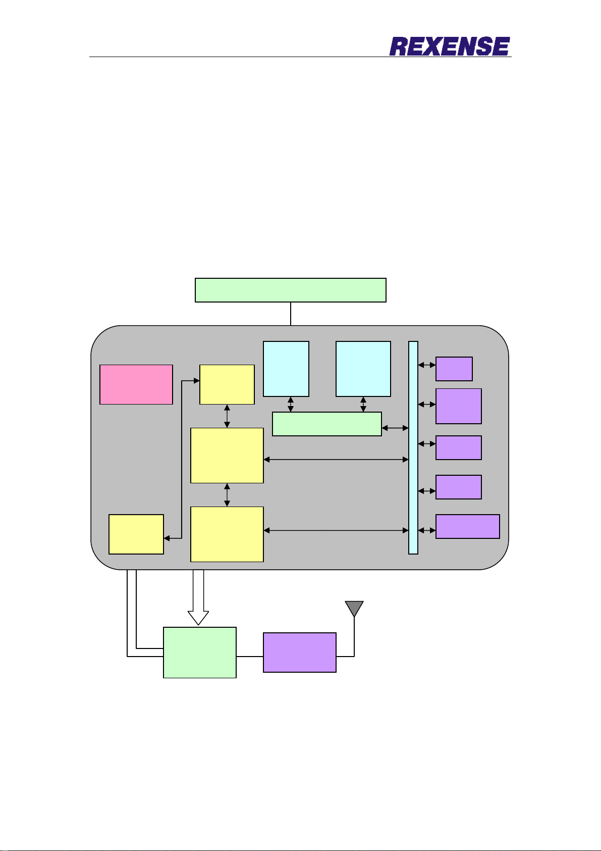
Figure 2-1.
Block Diagram
XTAL (Crystal Frequency 24MHz)
Power
Management
2.4GHz
Radio
ZigBee Chip
O-QPSK
Modem
IEEE802.15.4
MAC
Accelerator
128-bit AES
Encryption
Accelerator
Front-End
Module
Control
Data
SRAM
8kB
ARM CORTEX-M3
Matching
Network
Program
Flash
128kB
SPI
2-wire
serial
Timers
UART
12-bit ADC
Antenna
REX3SP Rexense 802.15.4/ ZigBee module complies with the FCC (Part 15), IC and ETSI
(CE) rules applicable to the devices radiating in uncontrolled environment.
REX3SP Rexense 802.15.4/ ZigBee module fully satisfies the requirements of the “Directive
2002/95/EC of the European Parliament and the Council of 27January 2003 on the
restriction of the use of certain hazardous substances in electrical and electronic
6
www.rexense.com

equipment” (RoHS).
To jumpstart evaluation and development, Rexense also offers a complete set of evaluation
and development tools. The ZigBee Development Kit comes with everything you need to
develop and test your own applications.
www.rexense.com
7
3. Specifications
3.1 Electrical Characteristics
3.1.1 Absolute Maximum Ratings
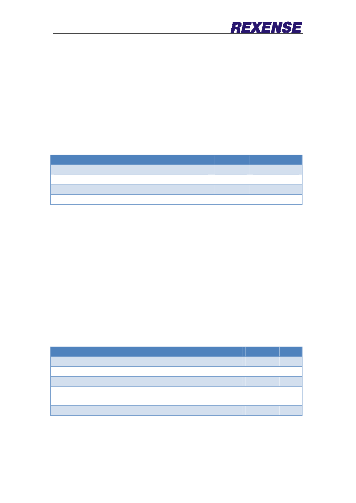
Table 3-1 Absolute Maximum Ratings
Parameters Min Max
Voltage on any pin, except RESET with respect to Ground -0.3V VDD_PADS 0.3
DC Current per I/O Pins
Total current into VDD/VDDA power lines (source)
RF Input Power
40 mA
150 mA
+15 dBm
Note:
Absolute Maximum Ratings are the values beyond which damage to the module may occur.
Under no circumstances must the absolute maximum ratings given in this table be violated.
Stresses beyond those listed under "Absolute Maximum Ratings" may cause permanent
damage to the module.
This is a stress rating only. Functional operation of the module at these or other conditions,
beyond those indicated in the operational sections of this specification, is not implied.
Exposure to absolute maximum rating conditions for extended periods may affect device
reliability.
3.1.2 Test Conditions
Table 3-2 Test conditions (unless otherwise stated), VCC = 3.3V, Tamb = 25°C
Parameters Range Unit
Supply Voltage, VCC 3.0 to 3.6 V
Current Consumption: RX mode 36 mA
Current Consumption: TX mode 170 mA
Current Consumption: Radio is turned off, MCU is active 50% of the
time
Current Consumption: Power-down mode 0.4 μA
9.0 mA
www.rexense.com
8
3.1.3 RF Characteristics
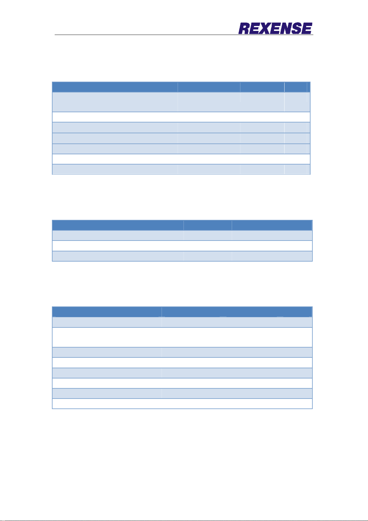
Table 3-3 RF Characteristics
Parameters Condition Range Unit
Frequency Band 2400 to
2483.5
Numbers of Channels 16
Channel Number 0B~1A Hex
Channel Spacing 5 MHz
Module Transmitter Output Power -32 to +20 dBm
Receiver Sensitivity PER=1% -104 dBm
TX Output/ RX Input Nominal Impedance For unbalanced output 50 Ω
MHz
3.1.4 Microcontroller Characteristics
Table 3-4. Microcontroller Characteristics
Parameters Condition Range Unit
On-chip Flash Memory size 128/192K bytes
On-chip RAM size 8/12K bytes
Operation Frequency 24 MHz
3.1.5 Module Interfaces characteristics
Table 3-5. Module Interfaces characteristics
Parameters Condition Range Unit
UART Maximum Baud Rate 230400 bps
ADC Resolution/ Conversion Time In single conversion
mode
ADC Input Resistance >1 MΩ
ADC Reference Voltage (VREF) 1.2 V
ADC Input Voltage 0 - VREF V
I2C Maximum Clock 400 kHz
GPIO Output Voltage (High/Low) -8/ 4 mA 2.8/ 0.9 V
Real Time Oscillator Frequency 32.768 kHz
12/4096 Bits/µs
www.rexense.com
9
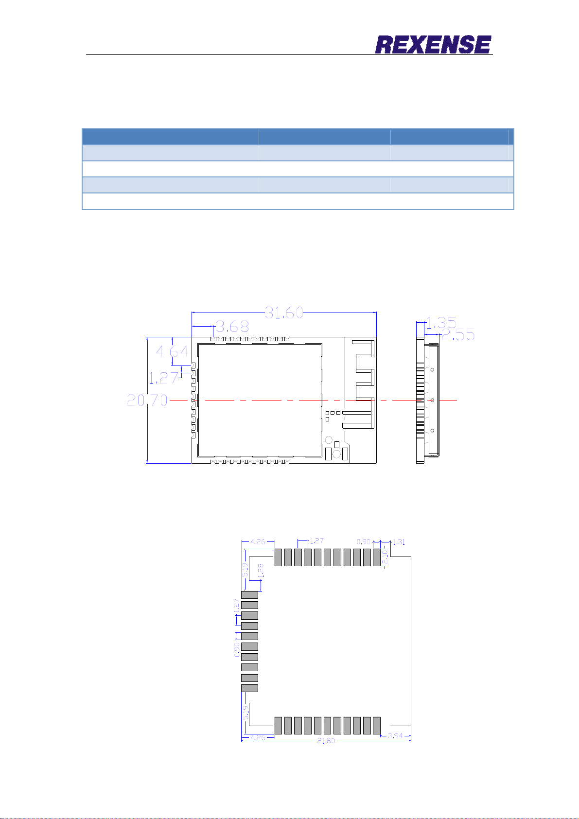
3.2 Physical/Environmental Characteristics and Outline
Table 3-6. Physical/Environmental Characteristics
Parameters Value Comments
Size 31.60*20.70*3.90mm
Weight 3.0g
Operating Temperature Range -40°C to +85°C
Operating Relative Humidity Range no more than 80%
Note: 1. Minor degration of clock stability may occur.
3.3 Pin Configuration
Figure 3-1. REX3SP Outline drawings
Figure 3-2. Recommended Footprint
www.rexense.com
The edge of the Mother Board
10

Figure 3-3. Pin Configuration
Table 3-7. Pin descriptions
Module
Pin No.
1
2
3 11
4 13 PC6 I/O Digital I/O;
QFN48
Pin
No.
Signal Direction Description
3.3V I DC3.3V supply
PC5 I/O
TX_ACTIV
E
O
Digital I/O;
Logic-level control for external Rx/Tx switch.
The MCU baseband controls TX_ACTIVE and
drives it high (VDD_PADS) when in Tx mode.
Select alternate output function with
GPIO_PCCFGH[7:4]
www.rexense.com
11

Module
Pin No.
QFN48
Pin
No.
Signal Direction Description
OSC32B I/O
nTX_ACTI
VE
O
32.768 kHz crystal oscillator Select analog
function with GPIO_PCCFGH[11:8]
Inverted TX_ACTIVE signal (see PC5) Select
alternate output function with
GPIO_PCCFGH[11:8]
PC7 I/O Digital I/O
5 14
OSC32A I/O
OSC32_EX
T
PA7
I Digital 32 kHz clock input source
I/O High
current
32.768 kHz crystal oscillator. Select analog
function with GPIO_PCCFGH[15:12]
Digital I/O. Disable REG_EN with
GPIO_DBGCFG[4]
Timer 1 Channel 4 output Enable timer
output with TIM1_CCER Select alternate
output function with GPIO_PACFGH[15:12]
Disable REG_EN with GPIO_DBGCFG[4]
Timer 1 Channel 4 input. (Cannot be
remapped.)
External regulator open drain output.
(Enabled after reset.)
6 18
TIM1_CH4
REG_EN O
O
I
7 12 nRESET I Active low chip reset (internal pull-up)
PB3 I/O Digital I/O
TIM2_CH3
8 19
UART_CTS I
SC1SCLK
O
I
O
I
Timer 2 channel 3 output Enable remap with
TIM2_OR[6] Enable timer output in
TIM2_CCER Select alternate output function
with GPIO_PBCFGL[15:12]
Timer 2 channel 3 input. Enable remap with
TIM2_OR[6].
UART CTS handshake of Serial Controller 1
Enable with SC1_UARTCFG[5] Select UART
with SC1_MODE
SPI master clock of Serial Controller 1 Either
disable timer output in TIM2_CCER or disable
remap with TIM2_OR[6] Enable master with
SC1_SPICFG[4] Select SPI with SC1_MODE
Select alternate output function with
GPIO_PBCFGL[15:12]
SPI slave clock of Serial Controller 1 Enable
slave with SC1_SPICFG[4] Select SPI with
www.rexense.com
12

Module
Pin No.
QFN48
Pin
No.
9 20
Signal Direction Description
SC1_MODE
PB4 I/O Digital I/O
Timer 2 channel 4 output Enable remap with
O
TIM2_CH4
I
TIM2_OR[7] Enable timer output in
TIM2_CCER Select alternate output function
with GPIO_PBCFGH[3:0]
Timer 2 channel 4 input. Enable remap with
TIM2_OR[7].
UART RTS handshake of Serial Controller 1
Either disable timer output in TIM2_CCER or
UART_RTS O
disable remap with TIM2_OR[7] Enable with
SC1_UARTCFG[5] Select UART with
SC1_MODE Select alternate output function
with GPIO_PBCFGH[3:0]
SPI slave select of Serial Controller 1 Enable
SC1nSSEL I
slave with SC1_SPICFG[4] Select SPI with
SC1_MODE
PA0 I/O Digital I/O
TIM2_CH1
10 21
SC2MOSI
PA1 I/O Digital I/O
11 22
TIM2_CH3 O
O
I
O
I
Timer 2 channel 1 output Disable remap with
TIM2_OR[4] Enable timer output in
TIM2_CCER Select alternate output function
with GPIO_PACFGL[3:0]
Timer 2 channel 1 input. Disable remap with
TIM2_OR[4].
SPI master data out of Serial Controller 2
Either disable timer output in TIM2_CCER or
enable remap with TIM2_OR[4] Enable
master with SC2_SPICFG[4] Select SPI with
SC2_MODE Select alternate output function
with GPIO_PACFGL[3:0]
SPI slave data in of Serial Controller 2 Enable
slave with SC2_SPICFG[4] Select SPI with
SC2_MODE
Timer 2 channel 3 output Disable remap with
TIM2_OR[6] Enable timer output in
TIM2_CCER Select alternate output function
with GPIO_PACFGL[7:4]
www.rexense.com
13

Module
Pin No.
QFN48
Pin
No.
Signal Direction Description
I
Timer 2 channel 3 input. Disable remap with
TIM2_OR[6].
TWI data of Serial Controller 2 Either disable
timer output in TIM2_CCER or enable remap
SC2SDA I/O
with TIM2_OR[6] Select TWI with
SC2_MODE Select alternate open-drain
output function with GPIO_PACFGL[7:4]
SPI slave data out of Serial Controller 2 Either
disable timer output in TIM2_CCER or enable
O
SC2MISO
remap with TIM2_OR[6] Enable slave with
SC2_SPICFG[4] Select SPI with SC2_MODE
Select alternate output function with
GPIO_PACFGL[7:4]
SPI master data in of Serial Controller 2
I
Enable slave with SC2_SPICFG[4] Select SPI
with SC2_MODE
PA2 I/O Digital I/O
TIM2_CH4
SC2SCL I/O
12 24
SC2SCLK
O
I
O
I
Timer 2 channel 4 output Disable remap with
TIM2_OR[7] Enable timer output in
TIM2_CCER Select alternate output function
with GPIO_PACFGL[11:8]
Timer 2 channel 4 input. Disable remap with
TIM2_OR[7].
TWI clock of Serial Controller 2 Either disable
timer output in TIM2_CCER or enable remap
with TIM2_OR[7] Select TWI with
SC2_MODE Select alternate open-drain
output function with GPIO_PACFGL[11:8]
SPI master clock of Serial Controller 2 Either
disable timer output in TIM2_CCER or enable
remap with TIM2_OR[7] Enable master with
SC2_SPICFG[4] Select SPI with SC2_MODE
Select alternate output function with
GPIO_PACFGL[11:8]
SPI slave clock of Serial Controller 2 Enable
slave with SC2_SPICFG[4] Select SPI with
SC2_MODE
13 25
www.rexense.com
PA3 I/O Digital I/O
SC2nSSEL I
SPI slave select of Serial Controller 2 Enable
slave with SC2_SPICFG[4] Select SPI with
14

Module
Pin No.
QFN48
Pin
No.
14 26
Signal Direction Description
SC2_MODE
Synchronous CPU trace clock Either disable
timer output in TIM2_CCER or enable remap
TRACECLK O
with TIM2_OR[5] Enable trace interface in
ARM core Select alternate output function
with GPIO_PACFGL[15:12]
Timer 2 channel 2 output Disable remap with
O
TIM2_CH2
I
TIM2_OR[5] Enable timer output in
TIM2_CCER Select alternate output function
with GPIO_PACFGL[15:12]
Timer 2 channel 2 input. Disable remap with
TIM2_OR[5].
PA4 I/O Digital I/O
ADC4 Analog
ADC Input 4. Select analog function with
GPIO_PACFGH[3:0].
Frame signal of Packet Trace Interface (PTI).
PTI_EN O
Disable trace interface in ARM core. Select
alternate output function with
GPIO_PACFGH[3:0].
Synchronous CPU trace data bit 2. Select
TRACEDA
TA2
O
4-wire synchronous trace interface in ARM
core. Enable trace interface in ARM core.
Select alternate output function with
GPIO_PACFGH[3:0].
15 27
www.rexense.com
PA5 I/O Digital I/O
ADC5 Analog
ADC Input 5. Select analog function with
GPIO_PACFGH[7:4].
Data signal of Packet Trace Interface (PTI).
PTI_DATA O
Disable trace interface in ARM core. Select
alternate output function with
GPIO_PACFGH[7:4].
nBOOTMO
DE
I
Embedded serial bootloader activation out of
reset. Signal is active during and immediately
after a reset on NRST.
Synchronous CPU trace data bit 3. Select
TRACEDA
TA3
O
4-wire synchronous trace interface in ARM
core. Enable trace interface in ARM core.
Select alternate output function with
GPIO_PACFGH[7:4]
15

Module
Pin No.
QFN48
Pin
No.
16 29
17 33
Signal Direction Description
PA6
I/O High
current
Digital I/O
Timer 1 channel 3 output Enable timer output
O
TIM1_CH3
I
in TIM1_CCER Select alternate output
function with GPIO_PACFGH[11:8]
Timer 1 channel 3 input (Cannot be
remapped.)
PC2 I/O Digital I/O Enable with GPIO_DBGCFG[5]
JTAG data out to debugger Selected when in
JTDO O
JTAG mode (default mode, see JTMS
description, Pin 35)
Serial Wire Output asynchronous trace
output to debugger Select asynchronous
trace interface in ARM core Enable trace
SWO O
interface in ARM core Select alternate output
function with GPIO_PCCFGL[11:8] Enable
Serial Wire mode (see JTMS description, Pin
35) Internal pull-up is enabled
PB1 I/O Digital I/O
SC1MISO O
SC1MOSI O
18 30
SC1SDA I/O
SC1TXD O
SPI slave data out of Serial Controller 1 Either
disable timer output in TIM2_CCER or disable
remap with TIM2_OR[4] Select SPI with
SC1_MODE Select slave with SC1_SPICR
Select alternate output function with
GPIO_PBCFGL[7:4]
SPI master data out of Serial Controller 1
Either disable timer output in TIM2_CCER or
disable remap with TIM2_OR[4] Select SPI
with SC1_MODE Select master with
SC1_SPICR Select alternate output function
with GPIO_PBCFGL[7:4]
TWI data of Serial Controller 1 Either disable
timer output in TIM2_CCER, or disable remap
with TIM2_OR[4] Select TWI with
SC1_MODE Select alternate open-drain
output function with GPIO_PBCFGL[7:4]
UART transmit data of Serial Controller 1
Either disable timer output in TIM2_CCER or
disable remap with TIM2_OR[4] Select UART
with SC1_MODE Select alternate output
www.rexense.com
16

Module
Pin No.
QFN48
Pin
No.
19 31
20 32
21 34
Signal Direction Description
function with GPIO_PBCFGL[7:4]
Timer 2 channel 1 output Enable remap with
O
TIM2_CH1
I
TIM2_OR[4] Enable timer output in
TIM2_CCER Select alternate output function
with GPIO_PACFGL[7:4]
Timer 2 channel 1 input. Disable remap with
TIM2_OR[4].
PB2 I/O Digital I/O
SPI master data in of Serial Controller 1
SC1MISO I
Select SPI with SC1_MODE Select master
with SC1_SPICR
SPI slave data in of Serial Controller 1 Select
SC1MOSI I
SPI with SC1_MODE Select slave with
SC1_SPICR
TWI clock of Serial Controller 1 Either disable
timer output in TIM2_CCER, or disable remap
SC1SCL I/O
with TIM2_OR[5] Select TWI with
SC1_MODE Select alternate open-drain
output function with GPIO_PBCFGL[11:8]
SC1RXD I
UART receive data of Serial Controller 1
Select UART with SC1_MODE
Timer 2 channel 2 output Enable remap with
O
TIM2_CH2
I
TIM2_OR[5] Enable timer output in
TIM2_CCER Select alternate output function
with GPIO_PBCFGL[11:8]
Timer 2 channel 2 input. Enable remap with
TIM2_OR[5].
Serial Wire clock input/output with debugger
SWCLK I/O
Selected when in Serial Wire mode (see JTMS
description, Pin 35)
JTAG clock input from debugger Selected
JTCK I
when in JTAG mode (default mode, see JTMS
description, Pin 35) Internal pull-down is
enabled
Digital I/O Either Enable with
PC3 I/O
GPIO_DBGCFG[5], or enable Serial Wire
mode (see JTMS description)
JTAG data in from debugger Selected when
JTDI I
in JTAG mode (default mode, see JTMS
description, Pin 35) Internal pull-up is
www.rexense.com
17

Module
Pin No.
QFN48
Pin
No.
22 35
23
36
Signal Direction Description
enabled
PC4 I/O Digital I/O Enable with GPIO_DBGCFG[5]
JTAG mode select from debugger Selected
when in JTAG mode (default mode) JTAG
JTMS I
mode is enabled after power-up or by forcing
NRST low Select Serial Wire mode using the
ARM-defined protocol through a debugger
Internal pull-up is enabled
Serial Wire bidirectional data to/from
debugger Enable Serial Wire mode (see JTMS
SWDIO I/O
description) Select Serial Wire mode using
the ARM-defined protocol through a
debugger Internal pull-up is enabled
PB0 I/O Digital I/O
VREF Analog O
ADC reference output. Enable analog
function with GPIO_PBCFGL[3:0].
ADC reference input. Enable analog function
VREF Analog I
with GPIO_PBCFGL[3:0]. Enable reference
output with an ST system function.
IRQA I External interrupt source A.
Synchronous CPU trace clock. Enable trace
TRACECLK O
interface in ARM core. Select alternate output
function with GPIO_PBCFGL[3:0].
24
38
www.rexense.com
TIM1CLK I Timer 1 external clock input.
TIM2MSK I Timer 2 external clock mask input.
PC1 I/O Digital I/O
ADC3 Analog
SWO O
TRACEDAT
A0
O
ADC Input 3 Enable analog function with
GPIO_PCCFGL[7:4]
Serial Wire Output asynchronous trace output to
debugger Select asynchronous trace interface in
ARM core Enable trace interface in ARM core
Select alternate output function with
GPIO_PCCFGL[7:4]
Synchronous CPU trace data bit 0 Select 1-, 2- or
4-wire synchronous trace interface in ARM core
Enable trace interface in ARM core Select alternate
output function with GPIO_PCCFGL[7:4]
18

Module
Pin No.
25
26
QFN48
Pin
No.
40
41
Signal Direction Description
PC0
JRST I
IRQD (1)
TRACEDAT
A1
PB7
ADC2 Analog
IRQC (1)
I/O High
current
I Default external interrupt source D
O
I/O High
current
I Default external interrupt source C
Digital I/O Either enable with GPIO_DBGCFG[5],
or enable Serial Wire mode (see JTMS description,
Pin 35) and disable TRACEDATA1
JTAG reset input from debugger Selected when in
JTAG mode (default mode, see JTMS description)
and TRACEDATA1 is disabled Internal pull-up is
enabled
Synchronous CPU trace data bit 1 Select 2- or
4-wire synchronous trace interface in ARM core
Enable trace interface in ARM core Select alternate
output function with GPIO_PCCFGL[3:0]
Digital I/O
ADC Input 2 Enable analog function with
GPIO_PBCFGH[15:12]
TIM1_CH2
PB6
ADC1 Analog
27
42
IRQB I External interrupt source B
TIM1_CH1
PB5 I/O Digital I/O
ADC0 Analog
28 43
TIM2CLK I Timer 2 external clock input
TIM1MSK I Timer 2 external clock mask input
29 NC
30
31
GND - Ground
32
Timer 1 channel 2 output Enable timer output in
O
I Timer 1 channel 2 input (Cannot be remapped)
I/O High
current
O
I Timer 1 channel 1 input (Cannot be remapped)
-
TIM1_CCER Select alternate output function with
GPIO_PBCFGH[15:12]
Digital I/O
ADC Input 1 Enable analog function with
GPIO_PBCFGH[11:8]
Timer 1 channel 1 output Enable timer output in
TIM1_CCER Select alternate output function with
GPIO_PBCFGH[11:8]
ADC Input 0 Enable analog function with
GPIO_PBCFGH[7:4]
No connect
www.rexense.com
19

Figure 3-4.Pins Control
Table 3-8. Logic control table
PA3: EXT_PA_EN PA6: LNA_BYPASS Description
0 X External PA and LNA Off
1 0 External PA On, LNA Off
1 1 External PA On, LNA On
PA7 Antenna Option
0 ANT1: PCB Antenna
1 ANT2: IPEX Output
Remarks:
PC5 is for the TX/RX switch of the external PA, must be set as alternate output pin.
halGpioConfig( PORTC_PIN(5), GPIOCFG_OUT_ALT );
Also, STM32W power mode must be set as alternate mode to enable the functionality of
the external PA.
ST_RadioSetPowerMode( ST_TX_POWER_MODE_ALTERNATE );
Please visit www.rexense.com to know the details.
www.rexense.com
20

3.4 Power Mode Configuration
This part helps users to configure the power mode of Rexense 802.15.4/ ZigBee module
(currently only supports STM32W Rexense 802.15.4/ ZigBee module) through UART.
Users can refer to our AT commands manual to complete the UART configuration through
serial port debugging software (such as AccessPort). The default UART baud rate of COO
and HHU is set as 115200-8-N-1; Router set as 9600-8-N-1. The normal function of UART
communication can be checked with command “AT+VER”. For more detailed AT commands,
please refer to www.rexense.com .
Acquire the current configuration information
Users can acquire the current configuration information of the module before UART
debugging with command ‘AT+GETINFO’.
Figure 3-3. AT+GETINFO
www.rexense.com
21

In Figure 3-3, parameters related with power mode configuration include:
Pwr=-03: The TX power of the chip is -3dBm;
PMode=0002: The wireless module works in External Power Amplifier Mode;
★Important Note:
z For standard Rexense 802.1 5.4/ ZigBee module, the TX power of the wireless
chip means the TX power of the module. It is recommended that the TX power set as
+07dBm to have better communication performance.
Chip
Module
z For enhanced Rexense 802.15.4/ ZigBee module, the TX power of the wireless
chip amplified by the power amplifier (PA) means the TX power of the module. It is
recommended that the TX power set as -03dBm or -5dBm;
Chip
PA
Ctrl
Module
The TX power of the wireless chip can be configured with the command “AT+ SETPWR”.
2. There are two power modes for Rexense 802.15.4/ ZigBee module, standard power
mode and external PA mode. As enhanced Rexense 802.15.4/ ZigBee module works in
external PA mode, user need to use command “AT+SETPWRMODE” to configure the
power mode of the Rexense 802.15.4/ ZigBee module.
z Standard Rexense 802.15.4/ ZigBee module works in standard power mode
configured by the command below:
AT+SETPWRMODE=0000
z Enhanced Rexense 802.15.4/ ZigBee module works in external PA mode configured
by the command below:
22
www.rexense.com

AT+SETPWRMODE=0002
External Antenna Configuration
For enhanced Rexense 802.15.4/ ZigBee module, there are two antenna options;
1. On-board PCB antenna;
2. U.FL (IPEX) Jack
z AT Command for on-board PCB antenna (please refer to 3.5.1 for more detailed
information of PCB antenna):
AT+SETANT=00
z If U.FL jack is used, it’s necessary to use the antenna cable and the SMA antenna at
the same time. (please refer to 3.5.3 for more detailed information of U.FL jack). The AT
command for U.FL jack:
AT+SETANT=01
www.rexense.com
23

3.5 Antenna Specifications
There’re 3 antenna options for the Standard Rexense 802.15.4/ ZigBee module (RX-32WS),
as shown below.
3.5.1 PCB Antenna
Figure 3-5. PCB Antenna
PCB Antenna
www.rexense.com
24

When PCB antenna output is selected, the following points should be noted:
1. Please avoid installing the module in a complete metal enclosure.
2. Please avoid placing high profile components next to antenna.
3. ZigBee module should not be placed next to consumer electronics which might interfere
with ZigBee's RF frequency band.
Figure 3-6. PCB Layout of the Proposed Antenna Selection
Area Supporting
the components
Metallization,wires, through
holes are unallowed
Metallization
The board design should prevent propagation of microwave field inside the board material.
Electromagnetic waves of high frequency may penetrate the board thus making the edges
of the board radiate, which may distort the antenna pattern.
To eliminate this effect, metalized and grounded holes must be placed around the board's
edges.
3.5.2 Steel Antenna
Figure 3-7. Steel Antenna
www.rexense.com
Steel Antenna
25

3.5.3 U.FL Jack to SMA Antenna
Figure 3-8. U.FL Jack
Note: when the U.FL (IPEX) jack is used, it’s necessary to use the antenna cable and the
SMA antenna at the same time. Please see the pictures for them as below.
Figure 3-9. Antenna Connective Cable
Antenna cable (AN11): cable length (11cm) and insertion loss (1dBi)
Figure 3-10. SMA Antenna
SMA antenna (AN2400): gain (2dBi)
U.FL Jack
www.rexense.com
26

Figure 3-11. Assembled Picture
www.rexense.com
27

3.6. Module Circuit Reference Design
3.6.1 SMD Module Reference Design (Single Voltage)
3.6.2 SMD Module Reference Design (Dual-Voltage)
www.rexense.com
28

3.7 Module Test Instructions
Figure 3-12. Standard JTAG Connection (1)
Figure 3-13. Standard JTAG Connection (2)
As shown in the above two figures, the first figure shows 20-pin JTAG interfaces and
module debugging& programming interfaces ; the second figure shows 10-pin JTAG
interfaces and module debugging and programming interfaces. So far, standard JTAG
29
www.rexense.com

connection is not supported for our products. Instead, we recommend the use of SWD
connection shown as follows.
Figure 3-14. SWD connection (1)
Figure 3-15. SWD connection (2)
www.rexense.com
30

Table 3-8. The relation between STM32W debugging & programming interfaces and JTAG
interfaces
20-pin
JTAG Interface
Pin Number (Name)
1(VCC) 1\2(VCC) 1(VCC) 1(VCC)
2(VCC) —— —— ——
3(nTRST) 3(nTRST) 3(nTRST) ——
4(GND) —— —— ——
5(JTDI) 5(JTDI) 4(JTDI) ——
6(GND) —— 5(GND) 5(GND)
7(JTMS) 7(JTMS) 7(JTMS) 7(SWDIO)
8(GND) 8(GND) —— ——
9(JTCK) 9(JTCK) 6(JTCK) 6(SWCLK)
10(GND) 10(GND) —— ——
11(RTCK) —— —— ——
12(GND) —— —— ——
13(JTDO) 6(JTDO) 2(JTDO) ——
14(GND) —— —— ——
15(RESET) 4(RESET) 8(RESET) 8(RESET)
16(GND) —— —— ——
17(DBGRQ) —— —— ——
18(GND) —— —— ——
19(DBGACK) —— —— ——
20(GND) —— —— ——
—— —— 9(PTI_EN) 9(PTI_EN)
—— —— 10(PTI_DATA) 10(PTI_DATA)
10-pin
JTAG Interface
Pin Number (Name)
10-pin module D&P
Interface JTAG
Pin Number (Name)
10-pin module D&P
Interface SWD
Pin Number (Name)
www.rexense.com
31

Figure 3-15. Module Program and Debug Interface Connection
nRES ET
3
4
5
8
11
9
7
6
2
20 P in JTAG Interface
12
13
14
15
16
17
18
19
20
21
PA2
PA3
PA4
PA5
PA6
PC2
PB1
PB2
SWCLK
PC3
PC5
PC6
PC7
PB3
PB4
PA010PA1
PC4/SWDIO22PB023PC124PC025PB726PB627PB528NC29GND30GND31GND
PA7
nRESET
VCC1VCC
U?
3.3V
SWDIO
SWCLK
nRES ET
JP?
1 2
3 4
5 6
7 8
9 10
11 12
13 14
15 16
17 18
19 20
32
SWDIO
SWCLK
3.8 Test Result of RF Performance
Figure 3-16. Receving sensitivity
SWD C onnection
www.rexense.com
32

Figure 3-17. Carrier Signal Testing
Figure 3-18. Modulating Signal Testing
www.rexense.com
33

p
4. Agency Certifications
FCC Certification
This equipment complies with Part 15 of the FCC rules and regulations.
To fulfill FCC Certification requirements, an OEM manufacturer must comply with the
following regulations:
1. The modular transmitter must be labeled with its own FCC ID number, and, if the FCC ID
is not visible when the module is installed inside another device, then the outside of the
device into which the module is installed must also display a label referring to the enclosed
module. This exterior label can use wording such as the following:
Example of label required for OEM product containing REX3SP 802.15.4/
ZigBee Module
Contains FCC ID: O46RY12M02
The enclosed device complies with Part 15 of the FCC Rules. Operation is subject to
the following two conditions: (1) this device may not cause harmful interference, and
(2) this device must accept any interference received, including interference that may
cause undesired o
Any similar wording that expresses the same meaning may be used.
2.
To be used with the REX3SP 802.15.4/ ZigBee Module, the external antennas have been
tested and approved which are specified in
ZigBee Module may be integrated with other custom design antennas which OEM installer
must authorize following the FCC 15.21 requirements.
WARNING: The Original Equipment Manufacturer (OEM) must ensure that the OEM
modular transmitter must be labeled with its own FCC ID number. This includes a clearly
visible label on the outside of the final product enclosure that displays the contents shown
below. If the FCC ID is not visible when the equipment is installed inside another device,
then the outside of the device into which the equipment is installed must also display a
label referring to the enclosed equipment.
IMPORTANT: This equipment complies with Part 15 of the FCC Rules. Operation is
subject to the following two conditions: (1) this device may not cause harmful interference,
and (2) this device must accept any interference received, including interference that may
cause undesired operation (FCC 15.19).
The internal/external antenna(s) used for this mobile transmitter must provide a
separation distance of at least 20cm from all persons and must not be co-located or
operating in conjunction with any other antenna or transmitter.
IMPORTANT: Modifications not expressly approved by this company could void the user's
authority to operate this equipment (FCC section 15.21).
For a Class B digital device or peripheral, the instructions furnished the user shall include
the following or similar statement, placed in a prominent location in the text of the manual:
NOTE: This equipment has been tested and found to comply with the limits for a Class B
digital device, pursuant to Part 15 of the FCC Rules. These limits are designed to provide
eration.
Approved Antenna List
. The REX3SP 802.15.4/
34
www.rexense.com

reasonable protection against harmful interference in a residential installation. This
equipment generates, uses and can radiate radio frequency energy and, if not installed
and used in accordance with the instructions, may cause harmful interference to radio
communications. However, there is no guarantee that interference will not occur in a
particular installation.
If this equipment does cause harmful interference to radio or television reception, which
can be determined by turning the equipment off and on, the user is encouraged to try to
correct the interference by one or more of the following measures:
-- Reorient or relocate the receiving antenna.
-- Increase the separation between the equipment and receiver.
-- Connect the equipment into an outlet on a circuit different from that to which the
receiver is connected.
-- Consult the dealer or an experienced radio/TV technician for help.
Approved Antenna List
REX3SP 802.15.4/ ZigBee Module has been tested and approved for use with the antennas
listed in the table below.
Table 4-1. Approved Antenna List
Min.
Separation
(cm)
Part Number Manufacturer Description
AN2400 Off the shelf
with SMA-J connector,
frequency range 2.4-2.5 GHz
Gain
(dBi)
Omni,
2 20
5. Contact Us
ZHEJIANG REXENSE TECHNOLOGY CO., LTD
Address: Room 105, No.7 Cuibai Road, Xihu District, Hangzhou 310012 P.R.China.
Tel: +86-571-85395623
Fax: +86-571-87987620
Email: sales@rexense.com
Webiste: www.rexense.com
www.rexense.com
35
 Loading...