


Leader in IOT Embedded Solution
LSD4RF0436-10D0
2.4GHz Wireless Module
LSD4RF0436-10D0 wireless module is a wireless module designed on the basis of TI RF integrated
chip CC2510. It is a high-performance 1mW IOT wireless transceiver. With the adoption of PCB antenna,
the module is compact and small in terms of overall design and can be widely used for short distance IOT
wireless communications in various applications. It is characterized by small volume, low power
consumption, long transmission distance, strong anti-interference capacity, low cost, etc.
Product Features
⚫ Working frequency range
- Working frequency range 2402~2480MHz
⚫ Multiple ways of modulation
- The ways of modulation including 2-FSK
are adopted to increase the capacity of
data anti-burst interference and random
interference
⚫ Power supply
- 2.0~3.6V (recommended to use 3.3V)
- I / O interface control level: 0~ VCC
⚫ High link budget
- High receiving sensitivity: -95 ± 1dBm
than 15m
⚫ Rapid channel switching
- < 90uS channel switching time, especially
suitable for FM communication system
⚫ Convenient for programming
- On-chip integrated 51 internal core, very
convenient for software programming
Applicable Situations
- Industrial remote sensing, telemetry
communication
- Home wireless security alarm system
- Personnel positioning system in mine
(@10KBaud)
- Transmit power: Max. 95.08dBμV /m
Super long transmission distance
- Excellent transmission performance,
reliable transmission distance is greater
Page 1 of 15
- Consumer electronic wireless applications,
wireless mouse keyboard, etc.

Leader in IOT Embedded Solution
Foreword
Zhejiang Lierda Internet of Things Technology Co.,Ltd provides the contents of the documentation to
support product design for its customer. The customers must design their products in accordance with the
specifications and parameters as mentioned in the documentation. The company will not assume any
liabilities for any personal injuries or property damages caused by improper operation of the customer.
Lierda Company has the right to update the documentation before the announcement is made. If you need
any help, please feel free to contact relevant personnel of our company or contact us via following
contacts:
Email: RF-Service@lierda.com
Forum: http://bbs.lierda.com/
Copyright Affirmation:
This documentation is copyrighted by Lierda Company and anyone will be legally responsible for
copying and reprinting the documentation without the permission of our company.
Copyright © Zhejiang Lierda Internet of Things technology Co.,Ltd, and all rights reserved.
Copyright © Zhejiang Lierda Internet of Things technology Co.,Ltd
Page 2 of 15

Revision Histories
Revision
Date
Author
Change Description
Rev01
June 14, 2019
You Xuecheng
Initial Revision
Leader in IOT Embedded Solution
Page 3 of 15

1. Specification Parameter
Major Parameter
Performance1
Remarks
Min.
Value
Typical
Value
Max.
Value
Working Voltage (V)
2.0
3.3
3.6
Working Temperature (℃)
-40 - 85
Initial Frequency Deviation
(KHz)
-40 - +40
Working Frequency Range
(MHZ)
2402
2480
The customer can customize the
working frequency
The customer can customize the
transmit power
Receiving sensitivity (dBm)
-
-95 - FSK modulation, PER <1%;
Deviation:38KHz,
Data rate: 10KBaud
Communication rate kBaud
1.2 - 500
2-FSK can be customized by the user
Ways of modulation
2-FSK
The programming may be customized
by the user
Type of interface
Stamp hole
Overall dimensions (mm)
(Refer to Drawing 2-1 for more
information)
-
Dimension accuracy
Grade GB / T 1804-C
In conformity with the requirements
of dimensional tolerance Grade C
Leader in IOT Embedded Solution
Form 1-1 Module Working Parameter1
Transmit power (dBμV /m)
95.08
1
The above testing conditions are as follows: temperature: 25°c , center frequency: 2433MHz and working voltage: 3.3V
Page 4 of 15

2. Dimensional Drawing and Interface Description
2.1 Module Dimensional Drawing
Leader in IOT Embedded Solution
Drawing 2-1 Dimensional Drawing for LSD4RF0436-10D0 PCBA (Unit: mm)
2.2 Real Module Drawing
Drawing 2-2 Real Module Drawing for LSD4RF0436-10D0
Page 5 of 15

Leader in IOT Embedded Solution
Module
Pin
Name
Function
Remarks
1
VDD
Power supply
2
D_CLK
Programmed
3
D_DATA
Programmed
4
RST
Reset
5
GND
Ground
6
GND
Ground
7
GND
Ground
8
P1_5
GPIO
9
P1_4
GPIO
10
P1_3
GPIO
11
P1_2
GPIO
12
GND
Ground
13
GND
Ground
14
GND
Ground
15
GND
Ground
16
RX
UART RX
17
TX
UART TX
18
GND
Ground
19
GND
Ground
2.3 Interface Description
The following figure shows the serial number of the pins of the module and describes the
corresponding pins:
Table 2-1 Functional Description of Pins of LSD4RF-10D0 Module
Page 6 of 15

Leader in IOT Embedded Solution
20
GND
Ground
21
GND
Ground
22
GND
Ground
23
VDD
Power supply
24
RST
Reset
25
P1_3
GPIO
26
P1_2
GPIO
27
RX
RX
28
TX
TX
29
VDD
Power supply
30
GND
Ground
2.4 PCB antenna instructions
The module has an on-board PCB antenna. During the layout of the board, please make sure the
area right below the antenna is completely clear, as shown in the following figure. The red part is the
user’s backplane area or the copper-clad area, the grey part is the clear area of the antenna of the
user’s backplane, and the boundary point of the clear area is the upper edge of the shielding cover.
Make sure there is no any metal in 360 degrees around the antenna; otherwise, the radiation efficiency
of the antenna will be affected, and the communication distance will be greatly affected.
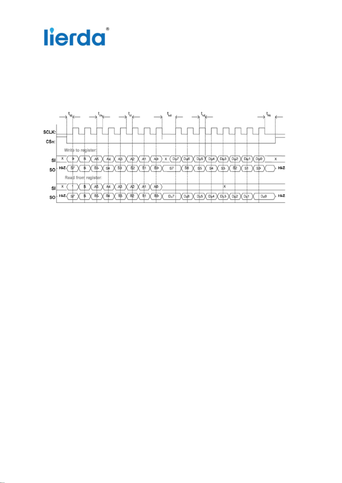
3. Basic Operation
Drawing 2-3 Description of Clear Area of Antenna
The module is installed on the user’s product. Since the module is equipped with MCU, it can be
Page 7 of 15
Leader in IOT Embedded Solution
directly operated via the built-in MCU control register and the transceiver buffer, which can complete the
receiving function of wireless data. The read-write operation timing sequence of the module register is
shown in the drawing. For more operation information, please refer to the latest data manual CC2510.
Drawing 3-1 SPI Timing Sequence
4. Frequently Asked Questions
4.1 The communications cannot be made if the module is at close range
⚫ To verify whether the sending and receiving configurations are matching and the communications
cannot be made if the configurations are different.
⚫ The voltage is abnormal; and the transmission will be abnormal if the voltage is too low.
⚫ The battery is low; and the transmission will be abnormal if the voltage is lowered due to the low
volume battery.
⚫ The RF signal does not reach the antenna or π circuit soldering occurs error if antenna welding is
abnormal.
4.2 Module communication distance is not enough
⚫ The power transmitted is small due to bad antenna impedance matching.
⚫ Objects such as metal around the antenna or the metal inside the module may cause serious signal
attenuation.
⚫ Any other interference signals in the test environment may cause the module to communicate
close.
Page 8 of 15

Leader in IOT Embedded Solution
⚫ Insufficient power supply will make the module’s transmit power abnormal.
⚫ Harsh test environment will make signal attenuation greater.
⚫ When the module communicates with other end after passing through the wall, the wall will have
a great impact on signal attenuation. The signal will be attenuated greatly when most of signals
are passing through the wall.
⚫ If the module is too close to the ground, resulting in poor communication due to being absorbed
and reflected.
5. Notation of Annexes
1. Recommended to use DC stabilized power supply to power for the module. The power ripple
coefficient should be as close as possible and the module needs to be reliably grounded. Please be
noted that the positive and negative poles of power supply shall be correctly connected. The
module may be permanently damaged if connected reversely.
2. Prohibited to have any metal objects around the module antenna. Otherwise, the communication
distance may be seriously affected.
Page 9 of 15

6. Packing
Technical Requirements
Reference Size
Technical requirements
1. The accumulative error per 10 drive holes should be within±0.2;
2. The inner bending of 250MM shall not be higher than 1;
3. Loaded with the materials: black PS and thickness: 0.30±0.05;
4. Surface impedance ranges from 106 to 1011 Ohm;
5. 23.5m per reel and packed in 13” plastic tray; the number of elements
accommodated:800 Pcs;
6. A0 and B0 shall be subject to the measurement made at the place 0.3mm away
from the lowest bottom inside the cavity, K0 is the inner depth and R angle
unmarked is 0.3;
7. The product complies with Standard EIA-481 ;
8. Product requirements comply with “ROHS”.
6.1 Ways of Packing
Leader in IOT Embedded Solution
■ Roll □ Foam □ ESD bag
Drawing 6-1 Roll Dimensional Drawing
Page 10 of 15

Leader in IOT Embedded Solution
Round Hole
Oval Hole
Protective Tape
Cover Tape
Round Hole
Recess
Oval Hole
Carrier Tape
Carrier Tape Rubber Wheel
Product Information Labeling
The diagram of roll wrapping module placement direction is as follows:
Drawing 6-2 Schematic Diagram of Module Placement
Drawing 6-3 Packaging Diagram
Page 11 of 15

Leader in IOT Embedded Solution
Regulatory Module Integration Instructions
List of applicable FCC rules
2.2
This device complies with part 15.247 of the FCC Rules.
2.3 Summarize the specific operational use conditions
This module can be used in Industrial remote sensing, telemetry communication
,Home wireless security alarm system. The input voltage to the module should be nominally 2.0~3.6
VDC ,typical value 3.3VDC and the ambient temperature of the module should not exceed 85℃.
This module using only one kind of antennas with maximum gain is 0.5dBi .Other antenna
arrangement is not covered by this certification.
The antenna is not field replaceable. If the antenna needs to be changed, the certification
should be re-applied.
2.4 Limited module procedures
Not applicable
2.5 Trace antenna designs
Not applicable
2.6 RF exposure considerations
This equipment complies with FCC radiation exposure limits set forth for an uncontrolled
environment .This equipment should be installed and operated with minimum distance
20cm between the radiator& your body. If the device built into a host as a portable usage,
the additional RF exposure evaluation may be required as specified by§ 2.1093.
2.7 Antennas
Module only contains one PCB antenna. No additional external connectors.
2.8 Label and compliance information
The outside of final products that contains this module device must display a label
referring to the enclosed module. This exterior label can use wording such as: “Contains
Transmitter Module FCC ID: 2AOFDLSD4RF043610D0 ”,or “Contains
FCC ID: 2AOFDLSD4RF043610D0 ”, Any similar wording that expresses the same
meaning may be used.
Page 12 of 15

Leader in IOT Embedded Solution
2.9 Information on test modes and additional testing requirements
a) The modular transmitter has been fully tested by the module grantee on the required
number of channels, modulation types, and modes, it should not be necessary for the
host installer to re-test all the available transmitter modes or settings. It is recommended
that the host product manufacturer, installing the modular transmitter, perform
some investigative measurements to confirm that the resulting composite
system does not exceed the spurious emissions limits or band edge limits (e.g., where a
different antenna may be causing additional emissions).
b) The testing should check for emissions that may occur due to the intermixing of
emissions with the other transmitters, digital circuitry, or due to physical properties of
the host product (enclosure). This investigation is especially important when integrating
multiple modular transmitters where the certification is based on testing each of them in
a stand-alone configuration. It is important to note that host product manufacturers
should not assume that because the modular transmitter is certified that they do not
have any responsibility for final product compliance.
c) If the investigation indicates a compliance concern the host product manufacturer is
obligated to mitigate the issue. Host products using a modular transmitter are subject to
all the applicable individual technical rules as well as to the general conditions of
operation in Sections 15.5, 15.15, and 15.29 to not cause interference. The operator of
the host product will be obligated to stop operating the device until the interference has
been corrected.
Below are steps for TX verification:
RfTest(); // RF parameter configuration
STX(); //Set RF to send mode
SIDLE() // Set RF to IDLE mode ,stop sending data
2.10 Additional testing, Part 15 subpart B disclaimer
The final host / module combination need to be evaluated against the FCC Part 15B
Page 13 of 15

Leader in IOT Embedded Solution
criteria for unintentional radiators in order to be properly authorized for operation as a Part
15 digital device.
The host integrator installing this module into their product must ensure that the final
composite product complies with the FCC requirements by a technical assessment or
evaluation to the FCC rules, including the transmitter operation and should refer to
guidance in KDB 996369.
Frequency spectrum to be investigated
For host products with certified modular transmitter, the frequency range of investigation
of the composite system is specified by rule in Sections 15.33(a)(1) through (a)(3), or the
range applicable to the digital device, as shown in Section 15.33(b)(1), whichever is the
higher frequency range of investigation.
Operating the host product
When testing the host product, all the transmitters must be operating.The transmitters can
be enabled by using publicly-available drivers and turned on, so the transmitters are
active. In certain conditions it might be appropriate to use a technology-specific call box
(test set) where accessory devices or drivers are not available.
When testing for emissions from the unintentional radiator, the transmitter shall be placed
in the receive mode or idle mode, if possible. If receive mode only is not possible then, the
radio shall be passive (preferred) and/or active scanning. In these cases, this would need
to enable activity on the communication BUS (i.e., PCIe, SDIO, USB) to ensure the
unintentional radiator circuitry is enabled. Testing laboratories may need to add attenuation or
filters depending on the signal strength of any active beacons (if applicable)
from the enabled radio(s). See ANSI C63.4, ANSI C63.10 and ANSI C63.26 for further
general testing details.
The product under test is set into a link/association with a partnering WLAN device, as per
the normal intended use of the product. To ease testing, the product under test is set to
transmit at a high duty cycle, such as by sending a file or streaming some media content.
Page 14 of 15

Leader in IOT Embedded Solution
FCC Statement
Any Changes or modifications not expressly approved by the party responsible for compliance could
void the user’s authority to operate the equipment. This device complies with part 15 of the FCC
Rules. Operation is subject to the following two conditions: (1)
This device may not cause harmful interference, and (2) This device must accept any interference
received, including interference that may cause undesired operation attenuation or filters depending
on the signal strength of any active beacons (if applicable) from the enabled radio(s). See ANSI
C63.4, ANSI C63.10 and ANSI C63.26 for further
The product under test is set into a link/association with a partnering WLAN device, as per the normal
intended use of the product. To ease testing, the product under test is set to transmit at a high duty
cycle, such as by sending a file or streaming some media content. ISED RSS Warning:
This device complies with Innovation, Science and Economic Development Canada licence-exempt
RSS standard(s). Operation is subject to the following two conditions:
(1) this device may not cause interference, and (2) this device must accept any interference, including
interference that may cause undesired operation of the device.
Le présent appareil est conforme aux CNR d'ISED applicables aux appareils radio exempts de
licence. L'exploitation est autorisée aux deux conditions suivantes:
(1) l'appareil ne doit pas produire de brouillage, et
(2) l'utilisateur de l'appareil doit accepter tout brouillage radioélectrique subi, même si le brouillage est
susceptible d'en compromettre le fonctionnement.
IC Label Instructions:
The outside of final products that contains this module device must display a label referring to the
enclosed module. This exterior label can use wording such as: “Contains Transmitter Module
IC: 25210-LSD043610D0”,or “Contains IC: 25210-LSD043610D0”, Any similar wording that
expresses the same meaning may be used.
L'extérieur des produits finis contenant ce module doit afficher une étiquette faisant référence au
module inclus. Cette étiquette extérieure peut utiliser des libellés tels que: contient le module
émetteur IC: 25210-LSD043610D0 ”ou“ contient: IC: 25210-LSD043610D0 ”, tout libellé similaire
exprimant lemême sens peut être utilisé.
Page 15 of 15
 Loading...