

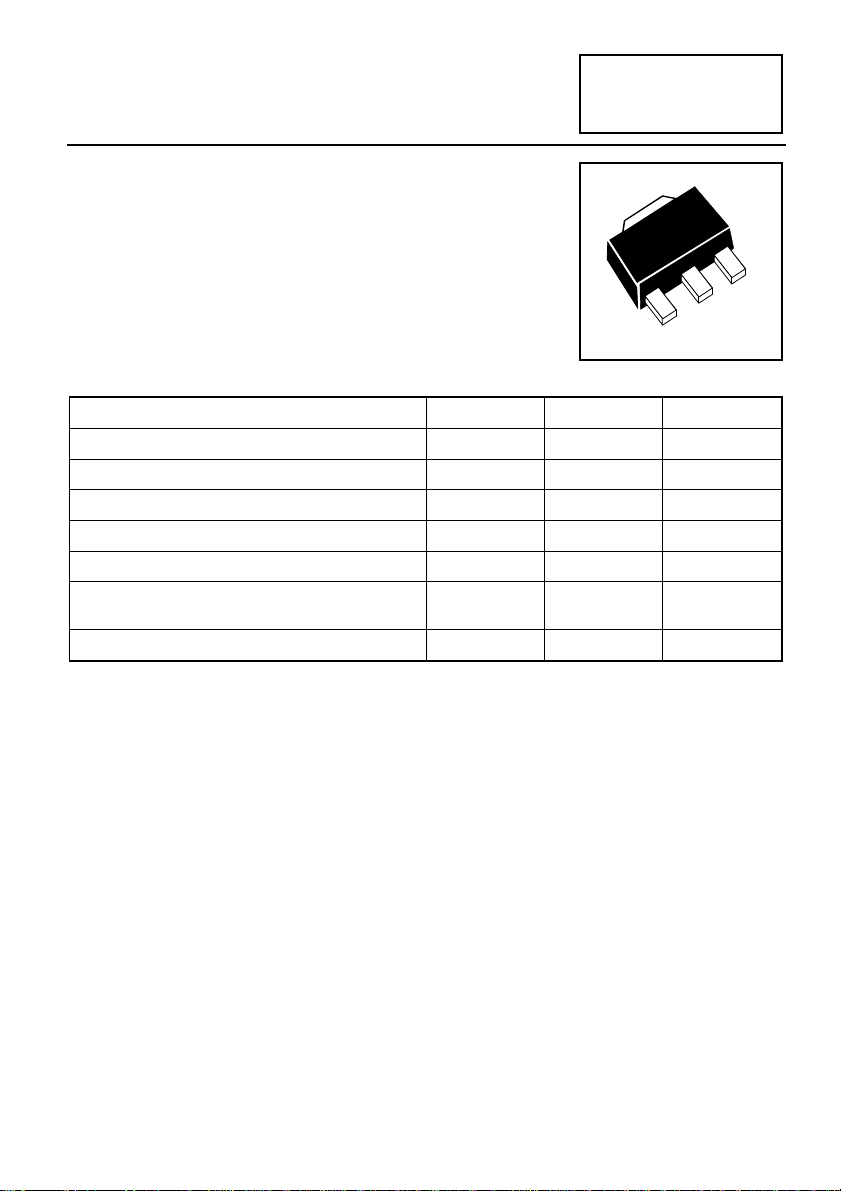
SOT89 NPN SILICON POWER
(SWITCHING) TRANSISTOR
ISSSUE 1 - DECEMBER 1998
FEATURES
* 2W POWER DISSIPATION
* 10A Peak Pulse Current
* Excellent H
* Extremely Low Saturation Voltage E.g. 17mv Typ.
* Extremely Low Equivalent On-resistance;
R
CE(sat)
Complimentary Type - FCX1151A
Partmarking Detail - 051
ABSOLUTE MAXIMUM RATINGS.
PARAMETER SYMBOL VALUE UNIT
Collector-Base Voltage V
Collector-Emitter Voltage V
Emitter-Base Voltage V
Peak Pulse Current ** I
Continuous Collector Current I
Power Dissipation at T
Operating and Storage Temperature Range T
† recommended P
‡ Maximum power dissipation is calculated assuming that the device is mounted on FR4
substrate measuring 40x40x0.6mm and using comparable measurement methods adopted by
other suppliers.
**Measured under pulsed conditions. Pulse width=300µs. Duty cycle ≤ 2%
Spice parameter data is available upon request for these devices.
Refer to the handling instructions for soldering surface mount components.
Characteristics up to 10 Amps
FE
57mΩ at 3A
CBO
CEO
EBO
CM
C
=25°C P
amb
calculated using FR4 measuring 15x15x0.6mm
tot
tot
j:Tstg
FCX1051A
C
C
B
150 V
40 V
5V
10 A
3A
1 †
2 ‡
-55 to +150 °C
W
W
E

FCX1051A
ELECTRICAL CHARACTERISTICS (at T
= 25°C unless otherwise stated).
amb
PARAMETER SYMBOL Min Typ Max UNIT CONDITIONS.
Collector-Base
Breakdown Voltage
Collector-Emitter
Breakdown Voltage
Collector-Emitter
Breakdown Voltage
Collector-Emitter
Breakdown Voltage
Emitter-Base
Breakdown Voltage
Collector Cut-Off Current I
Emitter Cut-Off Current I
Collector Emitter Cut-Off
Current
Collector-Emitter
Saturation Voltage
Base-Emitter
Saturation Voltage
Base-Emitter Turn-On
Voltage
Static Forward Current
Transfer Ratio
Transition Frequency f
Output Capacitance C
Switching Times
V
(BR)CBO
V
CES
V
CEO
V
CEV
V
(BR)EBO
CBO
EBO
I
CES
V
CE(sat)
V
BE(sat)
V
BE(on)
h
FE
T
obo
t
on
t
off
150 V
150 V
=100µA
I
C
=100µA
I
C
40 V IC=10mA
150 V
5V
=100µA, V
I
C
I
=100µA
E
0.3 10 nA VCB=120V
0.3 10 nA VEB=4V
0.3 10 nA V
17
85
140
170
250
25
120
180
250
340
mV
mV
mV
mV
mV
=120V
CES
IC=0.2A, IB=10mA*
I
=1A, IB=10mA*
C
I
=2A, IB=20mA*
C
I
=3A, IB=40mA*
C
I
=5A, IB=100mA*
C
880 1000 mV IC=3A, IB=40mA*
840 950 mV IC=3A, VCE=2V*
290
270
270
130
40
440
450
360
220
55
1200
IC=10mA, VCE=2V*
I
=1A, VCE=2V*
C
I
=3A, VCE=2V*
C
I
=5A, VCE=2V*
C
I
=10A, VCE=2V*
C
155 MHz IC=50mA, VCE=10V
f=100MHz
27 40 pF VCB=10V, f=1MHz
220 ns IC=3A, IB=30mA, VCC=10V
540 ns
I
=3A, I
C
=30mA, V
B
*Measured under pulsed conditions. Pulse width=300µs. Duty cycle ≤ 2%
=1V
EB
=10V
CC
 Loading...