

Zetex (Now Diodes) ZXMP2120E5 Schematic [ru]
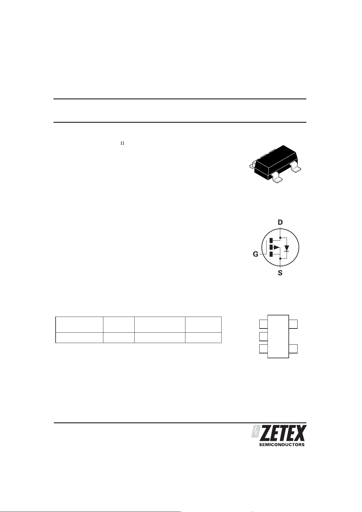
200V P-CHANNEL ENHANCEMENT MODE MOSFET
SUMMARY
(BR)DSS
=-200V; R
V
DESCRIPTION
This 200V enhancement mode P-channel MOSFET provides users with a
competitive specification offering efficient power handling capability, high
impedance and is free from thermal runaway and thermally induced
secondary breakdown. Applications benefiting from this device include a
variety of Telecom and general high voltage circuits.
= 28 ; ID= -122mA
DS(ON)
ZXMP2120E5
A 4 pin SOT223 version is also available (ZXMP2120G4).
FEATURES
High voltage
•
Low on-resistance
•
Fast switching speed
•
Low gate drive
•
•
Low threshold
•
SOT23-5 package variant engineered to increase spacing between
high voltage pins.
APPLICATIONS
•
Active clamping of primary side MOSFETs in 48 volt DC-DC converters
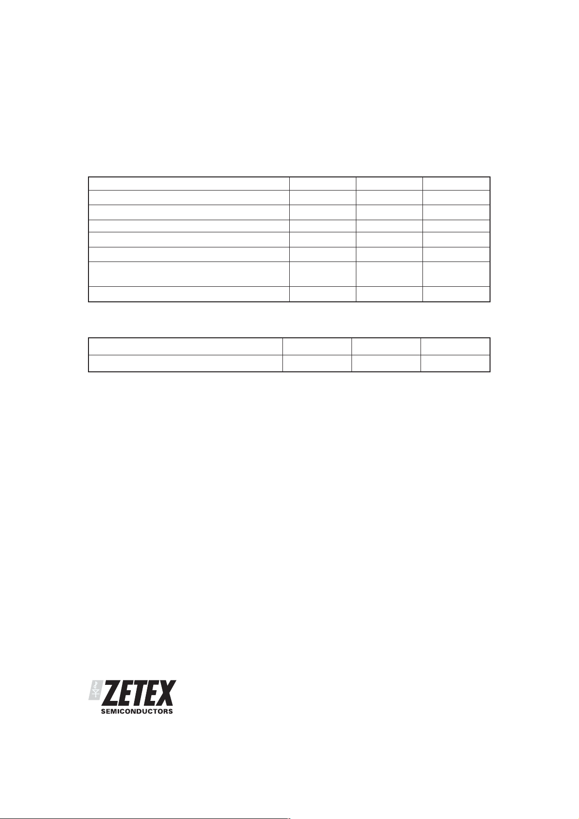
ORDERING INFORMATION
DEVICE REEL SIZE
ZXMP2120E5TA 7 8mm embossed 3,000 units
DEVICE MARKING
•
P120
(inches)
TAPE WIDTH (mm) QUANTITY
PER REEL
SOT23-5
N/C
D
N/C
PINOUT - TOP VIEW
S
G
ISSUE 2 - SEPTEMBER 2006
1
ZXMP2120E5
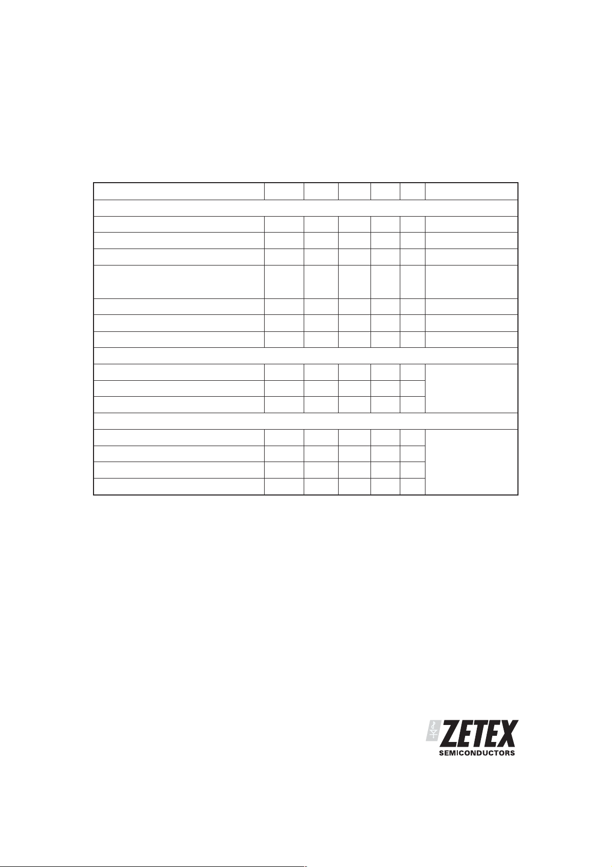
ABSOLUTE MAXIMUM RATINGS
PARAMETER SYMBOL LIMIT UNIT
V
(a)
I
I
I
P
DSS
GS
D
DM
SM
D
Drain-Source Voltage
Gate Source Voltage V
Continuous Drain Current (V
=10V; T
GS
amb
=25°C)
Pulsed Drain Current (c)
Pulsed Source Current (Body Diode)
Power Dissipation at T
amb
=25°C
(c)
(a)
Linear Derating Factor
Operating and Storage Temperature Range T
j:Tstg
THERMAL RESISTANCE
PARAMETER SYMBOL VALUE UNIT
Junction to Ambient
NOTES
(a) For a device surface mounted on 25mm x 25mm FR4 PCB with high coverage of single sided 1oz copper, in still air conditions
(b) For a device surface mounted on FR4 PCB measured at t⭐5 secs.
(c) Repetitive rating - pulse width limited by maximum junction temperature. Refer to Transient Thermal Impedance graph.
(a)
R
θJA
-200 V
±20
-122 mA
-0.7 A
-0.7 A
0.75
6
W
mW/°C
-55 to +150 °C
167 °C/W
V
ISSUE 2 - SEPTEMBER 2006
2
ZXMP2120E5
ELECTRICAL CHARACTERISTICS (at T
= 25°C unless otherwise stated)
amb
PARAMETER SYMBOL MIN. TYP. MAX. UNIT CONDITIONS.
STATIC
Drain-Source Breakdown Voltage V
Gate-Source Threshold Voltage V
Gate-Body Leakage I
Zero Gate Voltage Drain Current I
On-State Drain Current
Static Drain-Source On-State Resistance
Forward Transconductance
(1)
(1)
(1)(2)
(BR)DSS
GS(th)
GSS
DSS
I
D(on)
R
DS(on)
g
fs
-200 V ID=-1mA, VGS=0V
-1.5 -3.5 V ID=-1mA, VDS=V
20 nA VGS= ⫾20V, VDS=0V
-10
-100AµA
VDS=-200 V, VGS=0
V
=-160 V, VGS=0V,
DS
T=125°C
(2)
-300 mA VDS=-25 V, VGS=-10V
28
VGS=-10V, ID=-150mA
Ω
50 mS VDS=-25V,ID=-150mA
DYNAMIC
Input Capacitance
Output Capacitance
Reverse Transfer Capacitance
(2)
(2)
(2)
C
iss
C
oss
C
rss
100 pF
25 pF
7pF
V
=-25 V, VGS=0V,
DS
f=1MHz
SWITCHING
Turn-On Delay Time
Rise Time
(2)(3)
Turn-Off Delay Time
Fall Time
NOTES:
(1) Measured under pulsed conditions. Width=300µs. Duty cycle ≤ 2%.
(2) Sample test.
(3) Switching times measured with 50Ω source impedance and <5ns rise time on a pulse generator.
(2)(3)
(2) (3)
(2) (3)
t
d(on)
t
r
t
d(off)
t
f
7ns
15 ns
12 ns
15 ns
V
=-25V, ID=-150mA
DD
GS
ISSUE 2 - SEPTEMBER 2006
3
 Loading...