

Zetex (Now Diodes) ZXMHC3A01T8 Schematic [ru]
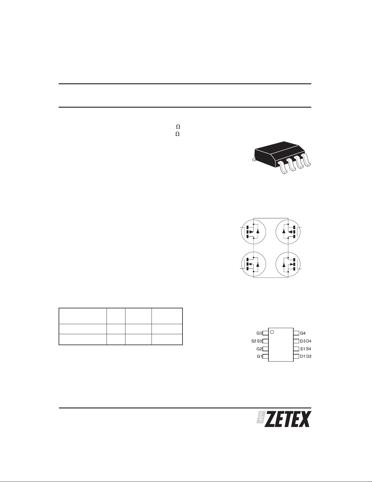
ZXMHC3A01T8
COMPLEMENTARY 30V ENHANCEMENT MODE MOSFET H-BRIDGE
SUMMARY
N-Channel = V
P-Channel = V
(BR)DSS
(BR)DSS
= 30V : R
= -30V : R
DESCRIPTION
This new generation of trench MOSFETs from Zetex
utilizesauniquestructurethatcombinesthebenefitsof
low on-resistance with fast switching speed. This
makes them ideal for high efficiency, low voltage,
power management applications.
FEATURES
Low on-resistance
•
Fast switching speed
•
Low threshold
•
•
Low gate drive
•
Single SM-8 surface mount package
= 0.12 ; ID= 3.1A
DS(on)
= 0.21 ; ID= -2.3A
DS(on)
G
1
D,1D
SM8
S
1
2
S
4
D,3D
G
4
4
APPLICATIONS
•
Single phase DC fan motor drive
ORDERING INFORMATION
DEVICE REEL
SIZE
ZXMHC3A01T8TA 7” 12mm 1,000 units
ZXMHC3A01T8TC 13” 12mm 4,000 units
TAPE
WIDTH
QUANTITY
PER REEL
DEVICE MARKING
•
ZXMH
C3A01
DRAFT ISSUE E - APRIL 2004
G
2
S
2
S
G
3
3
PINOUT
Top View
1
SEMICONDUCTORS
ZXMHC3A01T8
ABSOLUTE MAXIMUM RATINGS
PARAMETER SYMBOL N-Channel P-channel UNIT
Drain-source voltage V
Gate-source voltage V
Continuous drain current (V
= 10V; TA=25°C)
GS
(b)(d)
(VGS= 10V; TA=70°C)
(VGS= 10V; TA=25°C)
Pulsed drain current
Continuous source current (body diode)
Pulsed source current (body diode)
Power dissipation at T
(c)
=25°C
A
(b)
(c)
(a) (d)
(b)(d)
(a)(d)
I
I
I
I
P
DSS
GS
D
DM
S
SM
D
Linear derating factor
Power dissipation at T
A
=25°C
(b) (d)
P
D
Linear derating factor
Operating and storage temperature range T
j,Tstg
THERMAL RESISTANCE
PARAMETER SYMBOL VALUE UNIT
Junction to ambient
Junction to ambient
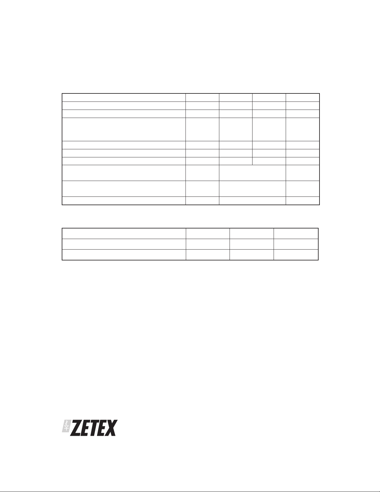
NOTES
(a) For a device surface mounted on 50mm x 50mm x 1.6mm FR4 PCB with high coverage of single sided 2oz copper, in still air conditions.
(b) For a device surface mounted on FR4 PCB measured at t ⱕ10 sec.
(c) Repetitive rating on 50mm x 50mm x 1.6mm FR4, D= 0.02, pulse width 300S - pulse width limited by maximum junction temperature. Refer
to transient thermal impedance graph.
(d) For device with one active die.
(a) (d)
(b) (d)
R
JA
R
JA
30 -30 V
±20 ±20 V
3.1
2.5
2.7
-2.3
-1.8
-2.0
14.5 -10.8 A
2.3 -2.2 A
14.5 -10.8 A
1.3
10.4
mW/°C
1.7
13.6
mW/°C
-55 to +150 °C
96 °C/W
73 °C/W
A
A
A
W
W
SEMICONDUCTORS
DRAFT ISSUE E - APRIL 2004
2
CHARACTERISTICS
ZXMHC3A01T8
DRAFT ISSUE E - APRIL 2004
3
SEMICONDUCTORS
ZXMHC3A01T8
N-channel
ELECTRICAL CHARACTERISTICS (at T
= 25°C unless otherwise stated)
amb
PARAMETER SYMBOL MIN. TYP. MAX. UNIT CONDITIONS
STATIC
Drain-source breakdown voltage V
Zero gate voltage drain current I
Gate-body leakage I
Gate-source threshold voltage V
Static drain-source on-state
resistance
Forward transconductance
DYNAMIC
(1)
(1) (3)
(3)
Input capacitance C
Output capacitance C
Reverse transfer capacitance C
SWITCHING
(2) (3)
Turn-on-delay time t
Rise time t
Turn-off delay time t
Fall time t
Total gate charge Q
Gate-source charge Q
Gate drain charge Q
(BR)DSS
DSS
GSS
GS(th)
R
DS(on)
g
fs
iss
oss
rss
d(on)
r
d(off)
f
g
gs
gd
30 V ID= 250A, VGS=0V
1.0 AVDS=30V, VGS=0V
100 nA VGS=±20V, VDS=0V
1.0 3.0 V ID= 250A, VDS=V
0.12
0.18
⍀
VGS= 10V, ID= 2.5A
V
⍀
= 4.5V, ID= 2.0A
GS
3.5 S VDS=4.5V, ID= 2.5A
190 pF
38 pF
20 pF
= 25V, VGS=0V
V
DS
f=1MHz
1.7 ns
V
2.3 ns
6.6 ns
= 15V, ID=2.5A
DD
R
≅ 6.0Ω ,VGS= 10V
G
2.9 ns
3.9 nC
0.6 nC
0.9 nC
V
= 15V, VGS= 10V
DS
I
= 2.5A
D
SOURCE-DRAIN DIODE
Diode forward voltage
Reverse recovery time
Reverse recovery charge
(1)
(3)
(3)
V
SD
t
rr
Q
rr
0.95 V Tj=25°C, IS= 1.7A,
V
GS
17.7 ns
13.0 nC
T
j
di/dt=100A/s
=0V
=25°C, IS= 2.5A,
GS
NOTES
(1) Measured under pulsed conditions. Pulse width ⱕ 300s; duty cycle ⱕ 2%.
(2) Switching characteristics are independent of operating junction temperature.
(3) For design aid only, not subject to production testing.
SEMICONDUCTORS
4
DRAFT ISSUE E - APRIL 2004
 Loading...