

Zetex (Now Diodes) ZXCT1008 Schematic [ru]
AUTOMOTIVE HIGH-SIDE CURRENT MONITOR
ZXCT1008
DESCRIPTION
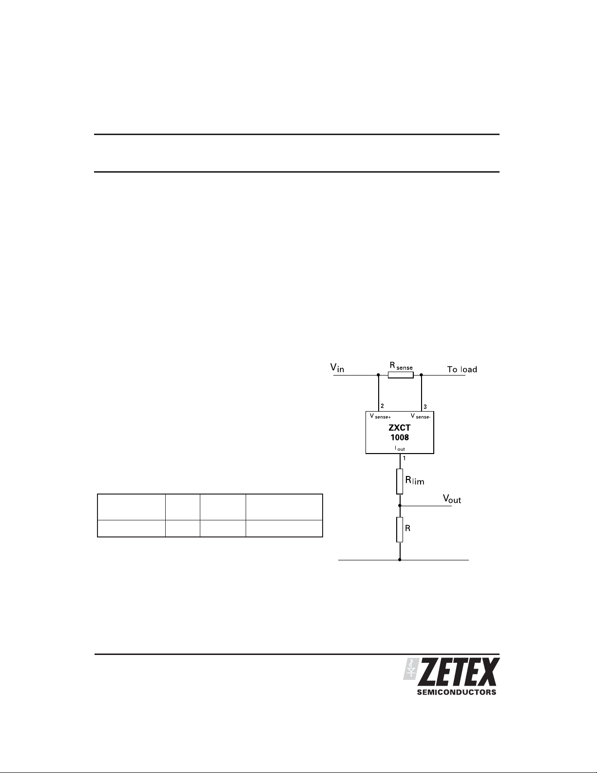
The ZXCT1008 is a high side current sense monitor.
Using this device eliminates the need to disrupt the
ground plane when sensing a load current.
It takes a high side voltage developed across a current
shunt resistor and translates it into a proportional
output current.
A user defined output resistor scales the output
current into a ground-referenced voltage.
The wide input voltage range of 20V down to as low as
2.5V make it suitable for a range of applications. The
ability to withstand high voltage transients and
reverse polarity connection, makes this part very
suitable for automotive and other transient rich
environments.
FEATURES
Low cost, accurate high-side current sensing
•
-40 to +125°C temperature range
•
•
Up to 500mV sense voltage
•
2.5V – 20V supply range
•
4µA quiescent current
•
1% typical accuracy
•
SOT23
APPLICATIONS
Automotive current measurement
•
DC motor and solenoid control
•
Over current monitor
•
Power management
•
APPLICATION CIRCUIT
ORDERING INFORMATION
DEVICE REEL
ZXCT1008FTA 7” 8mm 3,000 units
SIZE
TAPE
WIDTH
QUANTITY PER
DEVICE MARKING
•
108
ISSUE 4 - JULY 2007
REEL
1

ZXCT1008
ABSOLUTE MAXIMUM RATINGS
Voltage on any pin -0.6V to 20V (relative to I
Continuous output current, I
Continuous sense voltage, V
Operating temperature, T
, 10mA
OUT
†
, -0.5V to +5V
SENSE
,
A
-40 to 125°C
Storage temperature -55 to 150°C
Package power dissipation (T
Operation above the absolute maximum rating may cause device failure. Operation at the absolute maximum
ratings, for extented periods, may reduce device reliability.
= 25°C) 450mW Derate to zero at 150°C
A
ELECTRICAL CHARACTERISTICS
Test Conditions TA= 25°C, Vin= 5V, R
SYMBOL PARAMETER CONDITIONS LIMITS UNIT
V
in
I
out
V
sense
I
sense
1
VCCrange 2.5 20 V
Output current V
†
Sense voltage 0 500 mV
-V
sense
-
input current
Acc Accuracy
Gm Transconductance,
I
out/Vsense
BW Bandwidth V
1
Includes input offset voltage contribution
†
V
is defined as the differential voltage between V
SENSE
V
‡ -20dBm=63mVp-p into 50Ω
SENSE
= V
SENSE+
= VIN- V
= I
LOAD
LOAD
x R
- V
SENSE-
SENSE
out
sense
V
sense
V
sense
V
sense
V
sense
R
sense
V
sense
SENSE(DC)
V
SENSE(DC)
= 100Ω.
=0V
=10mV
=100mV
=200mV
=500mV
=0.1Ω
=200mV
= 10mV, Pin = -40dBm ‡
= 100mV, Pin = -20dBm ‡
SENSE+
and V
)
out
Min Typ Max
1
90
0.975
1.95
4.8
4
104
1.0
2.0
5.0
-2.5 2.5 %
10000 µA /V
300
2
.
SENSE-
15
120
1.025
2.05
5.2
µA
µA
mA
mA
mA
100 nA
kHz
MH
ISSUE 4 - JULY 2007
2
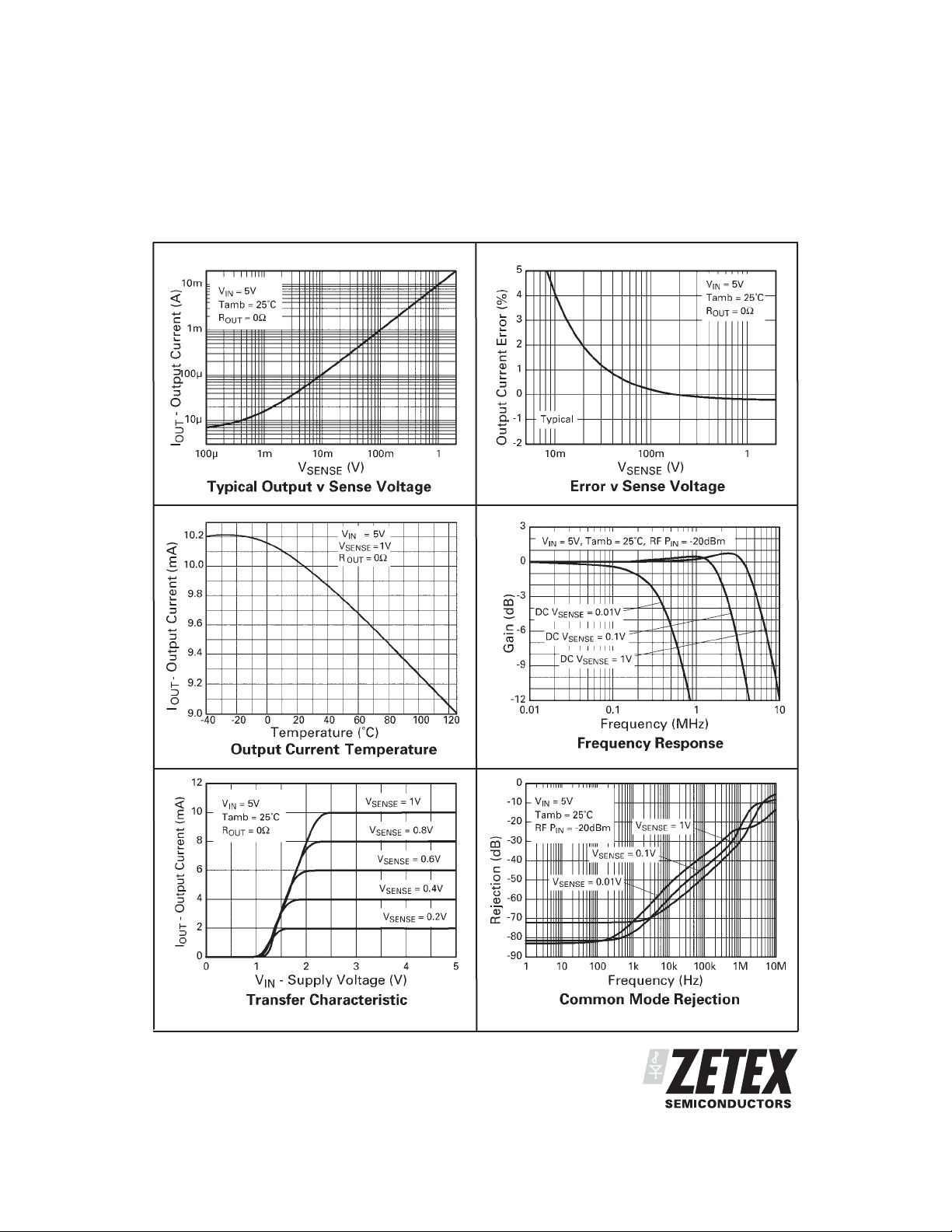
TYPICAL CHARACTERISTICS
ZXCT1008
ISSUE 4 - JULY 2007
3
 Loading...