

查询ZXM64N02X供应商
HIGH EFFICIENCY SIMPLESYNC PWM DC-DC CONTROLLERS
DESCRIPTION
The ZXRD1000 series provides complete control and
protection functions for a high efficiency (> 95%) DC-DC
converter solution. The choice of external MOSFETs allow
the designer to size devices according to ap plication. The
ZXRD1000 series uses advanced DC-DC converter
techniques to provide synchronous drive capability, using
innovative circuits that allow easy and cost effective
implementation of shoot through protection. The
FEATURES
• > 95% Efficiency
• Fixed frequency (adjustable) PWM
• Voltage mode to ensure excellent stability &
transient response
• Low quiescent current in shutdown mode,15µA
• Low battery flag
• Output down to 2.0V
• Overload protection
• Demonstration boards available
• Synchronous or non-synchronous operation
• Cost effective solution
• N or P channel MOSFETs
• QSOP16 package
ZXRD1000 SERIES
ZXRD1000 series can be used with an all N channel
topology or a combination N & P channel topology.
Additional functionality includes shutdown control, a
user adjustable low battery flag and simple
adjustment of the fixed PWM switching frequency.
The controller is available with fixed outputs of 5V or
3.3V and an adjustable (2.0 to 12V) output.
• Fixed 3.3, 5V and adjustable outputs
• Programmable soft st art
APPLICATIONS
• High efficiency 5 to 3.3V converters up to 4A
• Sub-notebook comp ut er s
• Embedded proce s s or power supply
• Distributed power supply
• Portable in s t ruments
• Local on card conversion
• GPS systems
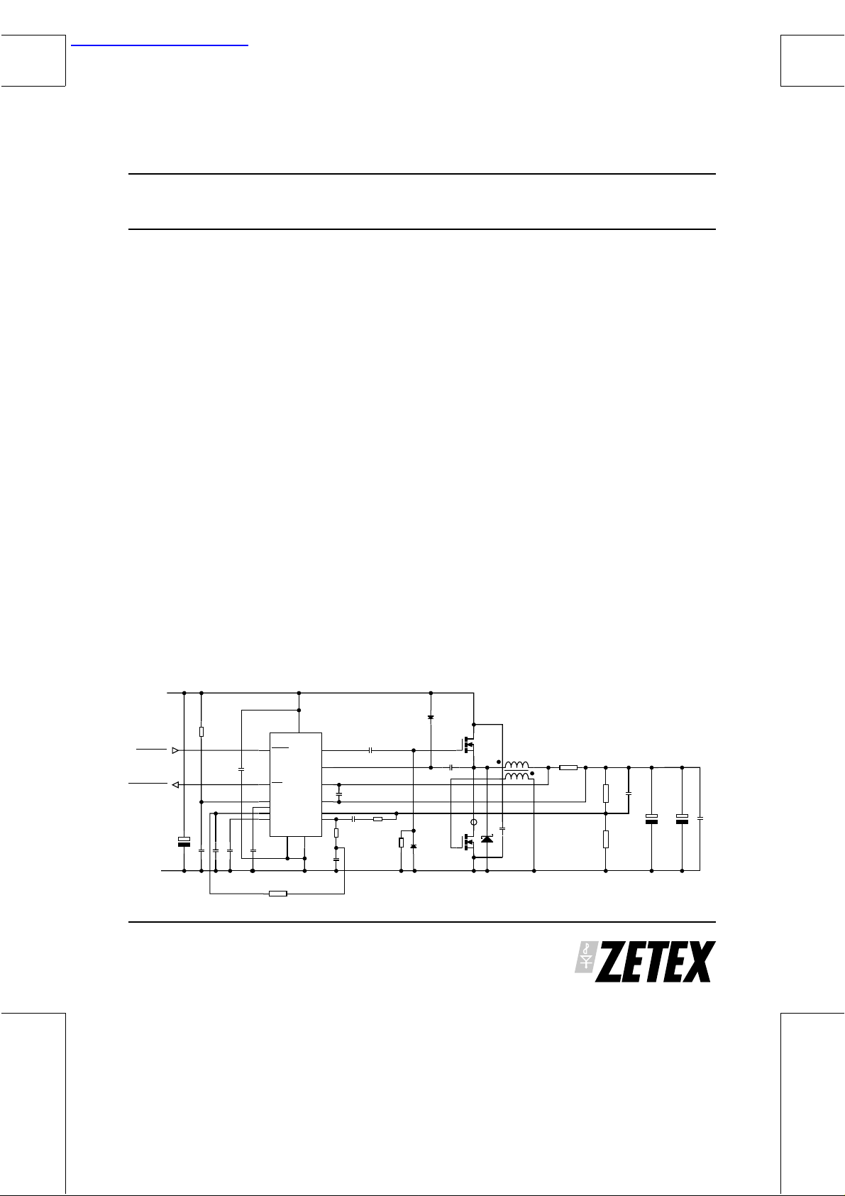
Very high efficiency SimpleSyncTM converter.
V
CC
4.5-10V
330pF
C3
IC1
13
V
IN
GNDG
V
DRIVE
Bootstrap
R
SENSE+
R
SENSE -
Comp
PWR
ND
34
2
1
7
C6
1µF
8
16
V
FB
15
CX1
R2
0.022µF
680R
C7
22µF
9
SHDN
C5
LB
SET
1µF
11
LBF
14
Delay
10
Decoup
6
V
INT
5
C
T
1µF
C4
R3
3k
Shut Down
Low input flag
68µF
R1
100k
C
IN
C2
C1
1µF
1µF
ISSUE 4 - OCTOBER 2000
D2
BAT54
ZXM64N02X
C11
1µF
N2
ZXM64N02X
N1
L1
15µH
Fx
C8
D1
2.2µF
ZHCS1000
R
0.01R
SENSE
R6
Cx2
10k
0.01µF
x2
680µF
R5
6k
C
OUT
120µF
V
3.3V 4A
OUT
C9
1µF
C10
1µF
RX
2k7
R4
D3
10k
BAT54
1
ZXRD1000 SERIES
ABSOLUTE MAXIMUM RATINGS
Input without bootstrap (P suffix) 20V
Input with bootstrap(N suffix) 10V
Bootstrap voltage 20V
Shutdown pin V
LB
pin V
SET
IN
IN
R
SENSE
+, R
SENSE -
V
IN
Power dissipation 610mW (Note 4)
Operating temperature -40 to +85°C
Storage temperature -55 to +125°C
ELECTRICAL CHARACTERISTICS
TEST CONDITIONS (Unless otherwise stated) T
Symbol Parameter Conditions Min Typ Max Unit
V
IN(min)
V
FB
(Note 1)
T
DRIVE
I
CC
f
osc
(Note 5)
f
osc(tol)
DC
MAX
V
RSENSE
V
CMRSENSE
LBF
SET
LBF
OUT
LBF
HYST
LBF
SINK
V
SHDN
I
SHDN
Min. Operating Voltage No Output Device 4.5 V
Feedback Voltage V
=5V,IFB=1mA 1.215 1.24 1.265 V
IN
4.5<V
50µA<I
Gate Output Drive Capability CG=2200pF(Note 2)
=1000pF
C
G
= 4.5V to maximim
V
IN
supply (Note 3)
Supply Current VIN=5V 1620mA
Shutdown Current V
SHDN
Operating frequency range
Frequency with timing capacitor C3=1300pF
=330pF
C
3
Oscillator Tol.
Max Duty Cycle N Channel
P Channel
R
voltage differentia l -40 to +85°C 50 mV
SENSE
Common mode range of V
RSENSE
-40 to +85°C 2 V
Low Battery Flag set voltage 1.5 V
Low Battery Flag output Active Low 0.2 0.4 V
Low Battery Fla g Hystere sis 10 20 50 mV
Low Battery Flag Sink Current -40 to +85°C 2 mA
Shutdown Threshold Voltage Low(off)
High(on) 1.5
Shutdown Pin Source Current 10
=25°C
amb
<18V 1.213 1.24 1.267 V
IN
<1mA,VIN=5V
FB
1.215 1.24 1.265 V
60
35
= 0V;VIN=5V 15 50
50
300 kHz
50
200
±25
15
0
94
100%%
IN
IN
0.25 V
ns
ns
µA
%
V
V
V
µA
Note 1. V
has a different function between fixed and adjustable controller options.
FB
Note 2. 2200pF is the maximum recommended gate capacitance.
Note 3. Maximum supply for P phase controllers is 18V,maximum supply for N phase controllers is 10V.
Note 4. See V
derating graph in Typical Characteristics.
IN
Note 5. The maximum frequency in this application is 300kHz. For higher frequency operation contact Zetex
Applications Department.
2
ISSUE 4 - OCTOBER 2000
ZXRD1000 SERIES
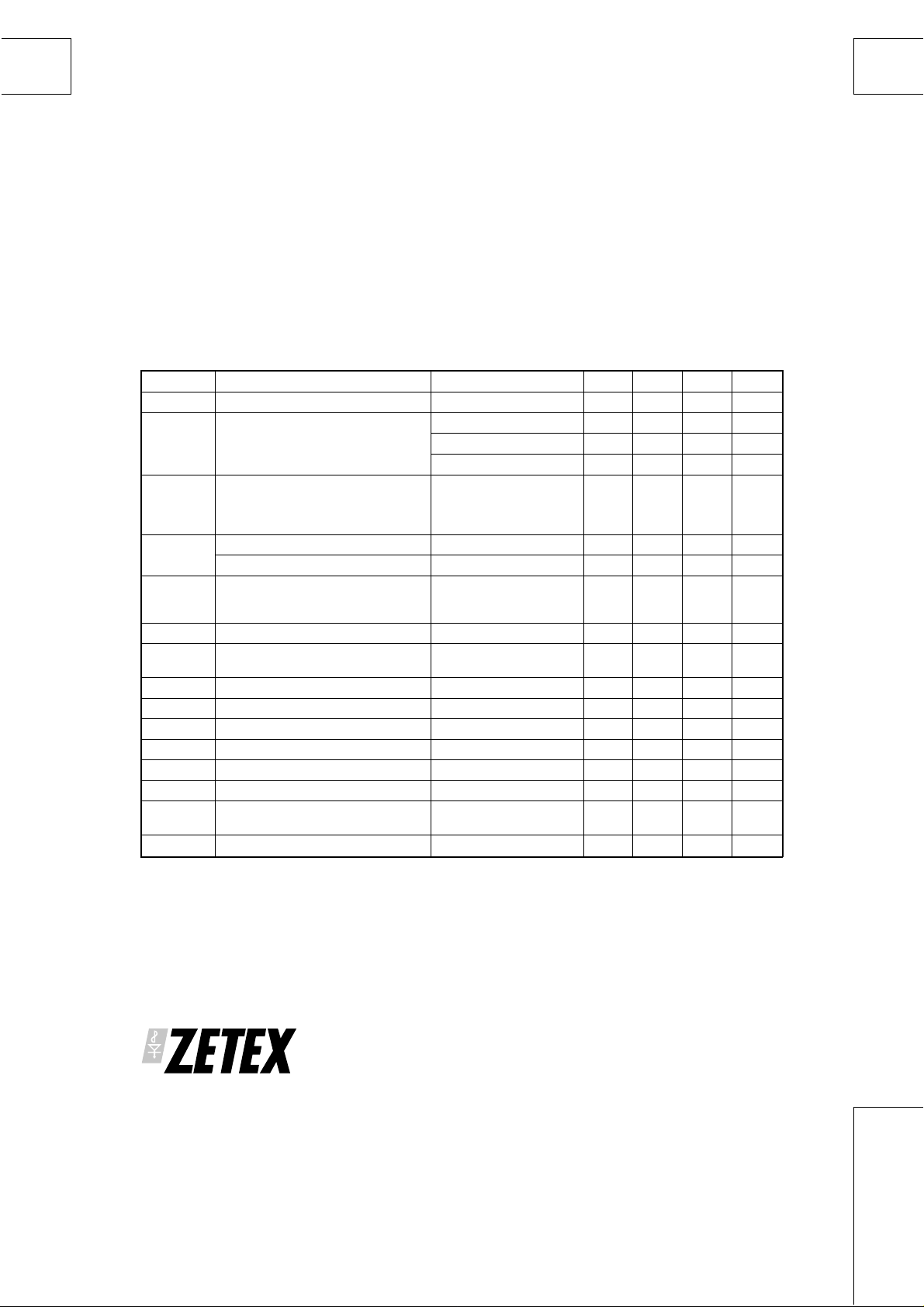
TYPICAL CHARACTERISTICS
202
201
200
(kHz)
199
OSC
F
198
197
4681012141618
VIN(V)
FOSC v VIN
1.244
1.242
(V)
1.24
FB
V
1.238
1.236
4681012141618
VIN (V)
VFB v VIN
C3=330pF
OUT
V
=3.3V
210
205
(kHz)
200
OSC
F
195
190
20
-40 -20 0 20 40 60 80 100
VIN=5V
C3=330pF
Temperature (°C)
FOSC v Temperature
1.25
VIN=5V
OUT
=3.3V
1.245
(V)
FB
V
1.235
20
V
1.24
1.23
-40 -20 0 20 40 60 80 100
Temperature (°C)
VFB v Temperature
1.02
SET
1.01
1.00
Normalised LB
0.99
4681012141618
Normalised LBSET v VIN
ISSUE 4 - OCTOBER 2000
VIN (V)
VIN=5V
1.005
SET
1.000
Normalised LB
0.995
20
-40 -20 0 20 40 60 80 100
Temperature (°C)
Normalised LBSET v Temperature
3
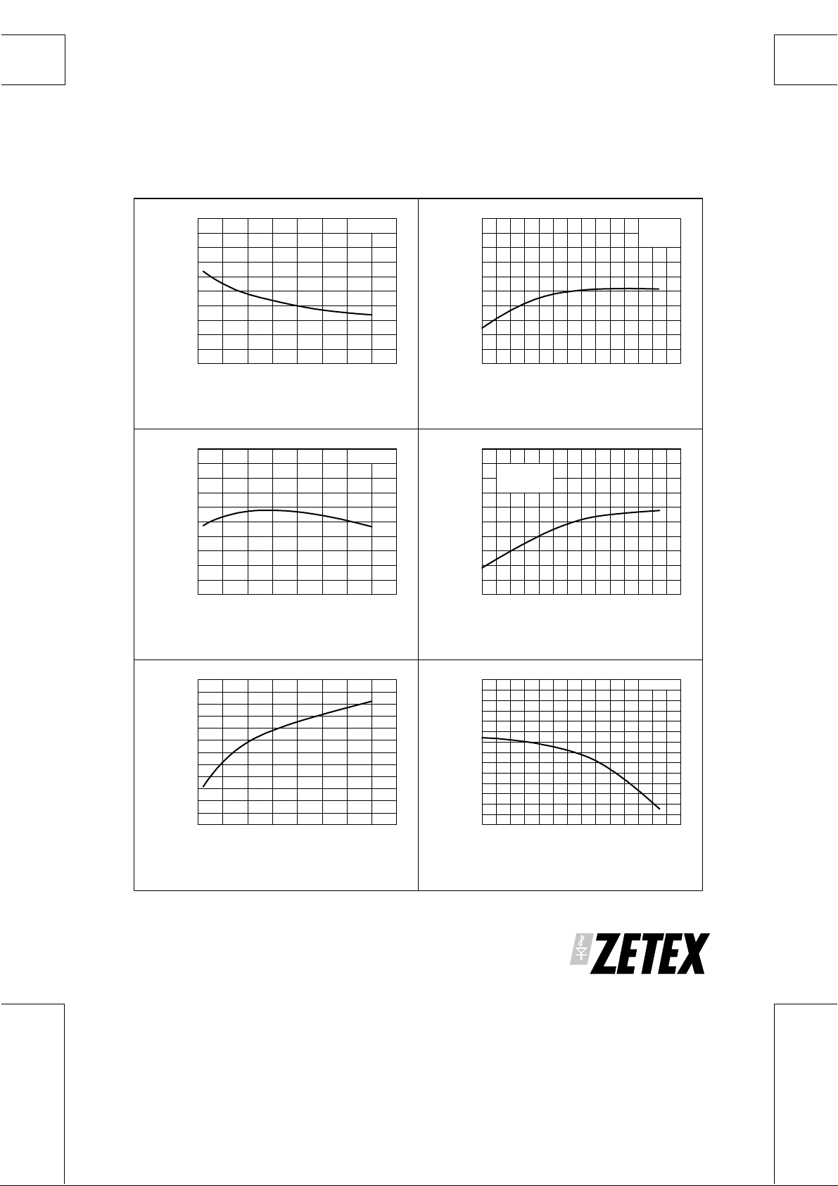
ZXRD1000 SERIES
TYPICAL CHARACTERISTICS
30
25
20
15
Supply Current (mA)
10
20
VIN(V)
Supply Current v V
IN
N Phase Device
300
200
(kHz)
OSC
F
100
0
100pF
1nF 10nF
Ti ming Capacitance
OSC
F
v Capacitance
Vin=5V
30
25
20
15
Supply Current (mA)
10
4 6 8 101214 1618
VIN(V)
Supply Current v V
P Phase Device
5
4
3
2
Current Lim i t (A )
1
0
0
VIN=5V
OUT=3.3V
V
10 20 30 40 50
RSENSE (m⍀)
Current Limit v R
204681012141618
IN
SENSE
20
15
(V)
IN
10
V
5
-40 -20 0 20 40 60 80 100
Temperature (°C)
VINDerating v Temperature
CG=2200pF
4
ISSUE 4 - OCTOBER 2000

DETAILED DESCRIPTION
The ZXRD1000 series can be configured to use either
N or P channel MOSFETs to suit most applications.
The most popular format, an all N channel
synchronous solution gives the optimum efficiency. A
feature of the ZXRD1000 series solution is the unique
method of ge nerating the synchronous driv e, called
SimpleSync . Most solutions use an additional
output from the controller, inverted and d elayed fr om
the main switch drive. The ZXRD1000 series solution
uses a simple overwindin g on the main ch oke (wound
on the same core at no real cost penalty) plus a small
ferrite bead . This means that the synchronous FET is
only enhanced when the main FET is turned off. This
reduces the ‘blanking period’ required for shootthrough protection, increasing efficiency and al lowing
smaller catch diodes to be used, making the controller
simpler and less costly by avoiding complex timing
circuitry. Included on chip are numerous f unctions that
allow flexibility to suit most applications. The nominal
switching frequency (200kHz) can be adjusted by a
simple timing capacitor, C3. A low battery detect circuit
is also provided. Off the shelf components are available
from major manufacturers such as Sumida to provide
either a single winding inductor for non-synchronous
applications or a coil with an over-winding for
synchronous applications. The combination of these
switching characteristics, innovative circuit design an d
excellent user flexibility, make the ZXRD1000 series
DC-DC solutions some of the smallest and most cost
effective and electrically efficient currently available.
Using Zetex’s HDMOS low R
for the main and synchronous switch, efficiency can
peak at upto 95% and remains high over a wide range
of operating currents. Programmabl e soft start can also be
adjusted via the capacitor, C7, in the compensation loop.
devices, ZXM64N02X
DS(on)
What is SimpleSyncTM?
Conventional Methods
In the conventional approach to the synchronous
DC-DC solution, much care has to be taken with the
timing constraints between the mai n and synchronous
switching devices. Not only is this dependent upon
individual MOSFET gate threshol ds (whic h vary from
device to device within data sheet limits and over
temperature), but it is also somewhat dependent upon
magnetics, layout and other parasitics. This normally
means that significant ‘dead time’ has to be factored
in to the design between the main and synchronous
devices being turned off and on respectively.
Incorrect application of dead time constraints can
potentially lead to catastrophic short circuit conditions
between V
and GND. For some battery operated
IN
ZXRD1000 SERIES
systems this can not only damage MOSFETs, but also
the battery itself. To realise correct ‘dead time’
implementation takes complex circuitry and hence
implies additional cost.
The ZETEX Meth od
Zetex has taken a different approach to solving these
problems. By looking at the basic architecture of a
synchronous converter, a nov el approach usin g the
main circuit inductor was developed. By taking the
inverse waveform found at the input to the main
inductor of a non-synchronous solution, a
synchronous drive waveform can be generated that is
always relative to the main drive waveform and
inverted with a small delay. This waveform can be
used to drive the synchronou s switch which means no
complex circuitry in the IC need be used to allow for
shoot-through protection.
Implementation
Implementation was very easy and low cost. It simply
meant peeling off a strand of the main inductor
winding and isolating it to form a coupled secondary
winding. These are available as standard items
referred to in the applications circuits parts list.The use
of a small, surface mount, inexpensive ’square loop’
ferrite bead provides an excellent method of
eliminating shoot-through due to variation in gate
thresholds. The bead essentially acts as a high
impedance for the few nano seconds that
shoot-through would normally occur. It saturates very
quickly as the MOSFETs attain steady state o peration,
reducing the bead impedance to virtually zero.
Benefits
The net result is an innovative solution that gives
additional benefits whilst lowering overall
implementation costs. It is also a technique that can
be simply omitted to make a non-synchronous
controller, saving further cost, at the expense of a few
efficiency points.
ISSUE 4 - OCTOBER 2000
5
ZXRD1000 SERIES
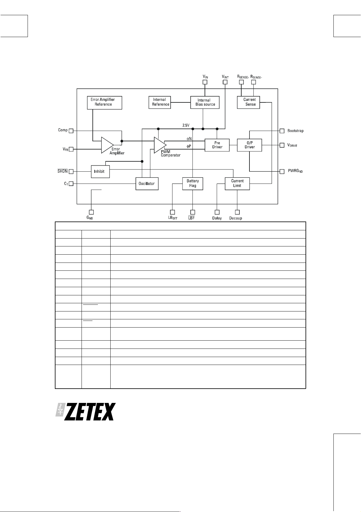
Functional Block Diagram
PIN DESCRIPTIONS ‡ See relevant Applications Section
Pin No. Name Description
1 Bootstrap Bootstrap circuit for generating gate drive
2V
DRIVE
3PWRG
4G
5C
6V
7R
8R
9
ND
T
INT
SENSE+
SENSE-
SHDN Shutdown control. Active low.
10 Dec o up Optional short circuit and overloa d decoupling capaci tor for increased accurac y
11
12 LB
13 V
LBF Low battery flag output. Active low, open collector output
SET
IN
14 Delay External R and C to set the desired cycle time for hiccup circuit. ‡
15 Comp Compensation pin to allow for stability components and soft start. ‡
16 V
FB
Output to the gate drive circuit for main N/P channel switches
Power ground
ND
Signal ground
Timing Capacitor sets oscillator frequency. ‡
Internal Bias Circuit. Decouple with 1µF ceramic capacitor
Higher potential input to the current sense for current limit circuit
Lower potential input to the current sense for current limit circuit
Low battery flag set. Can be connected to VIN if unused, or threshold set
via potential divider. ‡
Input Voltage
Feedback Voltage. This pin has a different function between fixe d and
adjustable controller options. The appropriate controller must be used for
the fixed or adjustable solution. Connect to V
potential divider for adjustable output. ‡
for fixed output, or to
OUT
6
ISSUE 4 - OCTOBER 2000

ZXRD1000 SERIES
Applications
Note: Component names refer to designators shown
in the application circuit diagrams.
Output Capacitors
Output capacitors are a critical choice in the overall
performance of the solution. T hey are required to filter
the output and supply load transi ent curren t. They are
also affected by the switching frequency, ripple
current, di/dt and magnitude of transient load current.
ESR plays a key role in determining the value of
capacitor to be used. Combination of both high
frequency, low value ceramic capacitors and low ESR
bulk storage capacitors optimised for switching
applications provide the best response to load
transients and ripple requirements. Electrolytic
capacitors with low ESR are larger and more
expensive so the ultimate choice is always a
compromise between size, cost and performance.
Care must also be taken to ensure that for large
capacitors, the ESL of the leads does not become an
issue. Excellent low ESR tantalum or electrolytic
capacitors are available from Sanyo OS-CON, AVX,
Sprague and Nichicon.
The output capacitor will also affect loop stability,
transient performance. The capacitor ESR should
preferably be of a similar value to the sense resistor.
Parallel devices may be required.
I
RIPPLE(RMS)
=
0.29 V
OUT
L f V
(VIN−V
where L= output filter inductance
f= switching frequency
For output vol t a ge ripple it is neces s a ry to know the
peak ripple current which is given by:
V
( VIN− V
I
pk−pk
=
OUT
L f V
OUT)
IN
Voltage ripple is then:V
= I
−
RIPPLE
∗ ESR
pk
pk
)
OUT
IN
Input Capacitors
The input capacitor is chosen for its RMS current and
voltage rating. The use of low ESR electrolytic or
tantalum capacitors is recommended. Tantalum
capacitors should have their voltage rating at 2V
(max), electrolytic at 1.4VIN(max). I
can be
RMS
approximated by:
I
RMS
= I
OUT
(V
OUT(VIN−VOUT
V
))
IN
√
Underspecification of this parameter can affect long
term reliability. An additonal ceramic capacitor should
be used to provide high frequency decoupling at V
IN.
Also note that the input capacitance ESR is effectively in
series with the input and hence contributes to efficiency
losses related to I
2
* ESR of the input capacitor.
RMS
MOSFET Selection
The ZXRD1000 family can be configured in circuits
where either N or P channel MOSFETs are employed
as the main switch. If an N channel device is used, the
corresponding N phase controller must be chosen.
Similarly, for P channel main switch a P phase
controller must be used. The ordering information has
a clear identifier to distinguish between N and P phase
controllers.
The MOSFET selection is subject to thermal and gate
drive considerations. Care also has to be taken to allow
for transition losses at high input voltages as well as
R
losses for the main MOSFET. It is
DS(ON)
recommended that a device with a drain source
breakdown of at least 1.2 times the maximum V
should be used.
For optimum efficiency , two N channel low R
DS(on)
devices are required. MOSFETs should be selected
with the lowest R
consistent with the output
DS(ON)
current required. As a guide, for 3-4A output, <50mΩ
devices would be optimum, provided the devices are
low gate threshold and low gate charge. Typically look
for devices that will be fully enhanced with 2.7V V
GS
for 4-5A capability.
Zetex offers a range of low R
logic level MOSFETs
DS(ON)
which are specifically designed with DC-DC power
conversion in mind. Packaging includes SOT23,
SOT23-6 and MSOP8 options. Ideal examples of
optimum devices would be Zetex ZXM64N03X and
ZXM64N02X (N channel). Contact your local Zetex office
or Zetex web pag e for further information.
IN
IN
ISSUE 4 - OCTOBER 2000
7
ZXRD1000 SERIES
Applications (continued)
Inductor Selection
The inductor is one of the most critical componen ts in
the DC-DC circuit.There are numerous types of devi ces
available from many suppliers. Zetex has opted to
specify off the shelf encapsulated surface mount
components, as these represent the best compromi se
in terms of cost, size, performance and shielding.
The SimpleSync
with an overwinding for the gate drive which is
available as a standard part. However, for engineers
who wish to design their own custom magnetics, this
is a relatively simple and low cost construction
technique. It is simply forme d by terminating on e of
the multiple strands of litz type wire separ ately. It is
still wound on the same core as the main winding and
only has to handle enough current to charge the gate
of the synchronous MOSFET. The major benefit is
circuit simplification and hence lower cost of the co ntrol
IC. For non-synchronous operation, the overwinding is
not required.
The choice of core type also plays a key role. For
optimum performance, a ’swinging choke’ is often
preferred. This is one which exhibits an increase in
inductance as load current decreases. This has the net
effect of reducing circulating current at lighter load
improving efficiency. There is normally a cost
premium for this added benefit. For this reason the
chokes specified are the more usual constant
inductance type.
Peak current of the inductor should be rated to
minimum 1.2I
winding resistance of the main inductor should be less
than the main switch output on resistance.
Schottky Diode
Selection depends on whether a synchronous or
non-synchronous approach is taken. For the
ZXRD1000, the unique approach to the synchronous
drive means minimal dead time and hence a small
SOT23 1A DC rated device will suffice, such as the
ZHCS1000 from Zetex. The device is o nly d esigned to
prevent the body diode of the synchronous MOSFET
from conducting dur i ng the initial swit c hing transient
until the MOSFET takes over. The device should be
connected as close as possible to the source terminals
of the main MOSFET.
For non-synchron ous applications , t he Schottky diode
must be selected to allow for the worst case
TM
technique uses a main inductor
(max) . To maximise efficiency, the
OUT
conditions, when V
is at its highest and V
IN
OUT
is
lowest (short circuit conditions for example). Under
these conditions the device must handle peak current
at close to 100% duty cycle.
Frequency Adjustment
The nominal runnin g frequency of th e controll er is set
to 200kHz in the applications shown. This can be
adjusted over the range 50kHz to 300kHz by changing
the value of capacitor on the C
pin. A low cost
T
ceramic capacitor can be used.
Frequency = 60000/C3 (pF)
Frequency v temperature is given in the typical
characteristics.
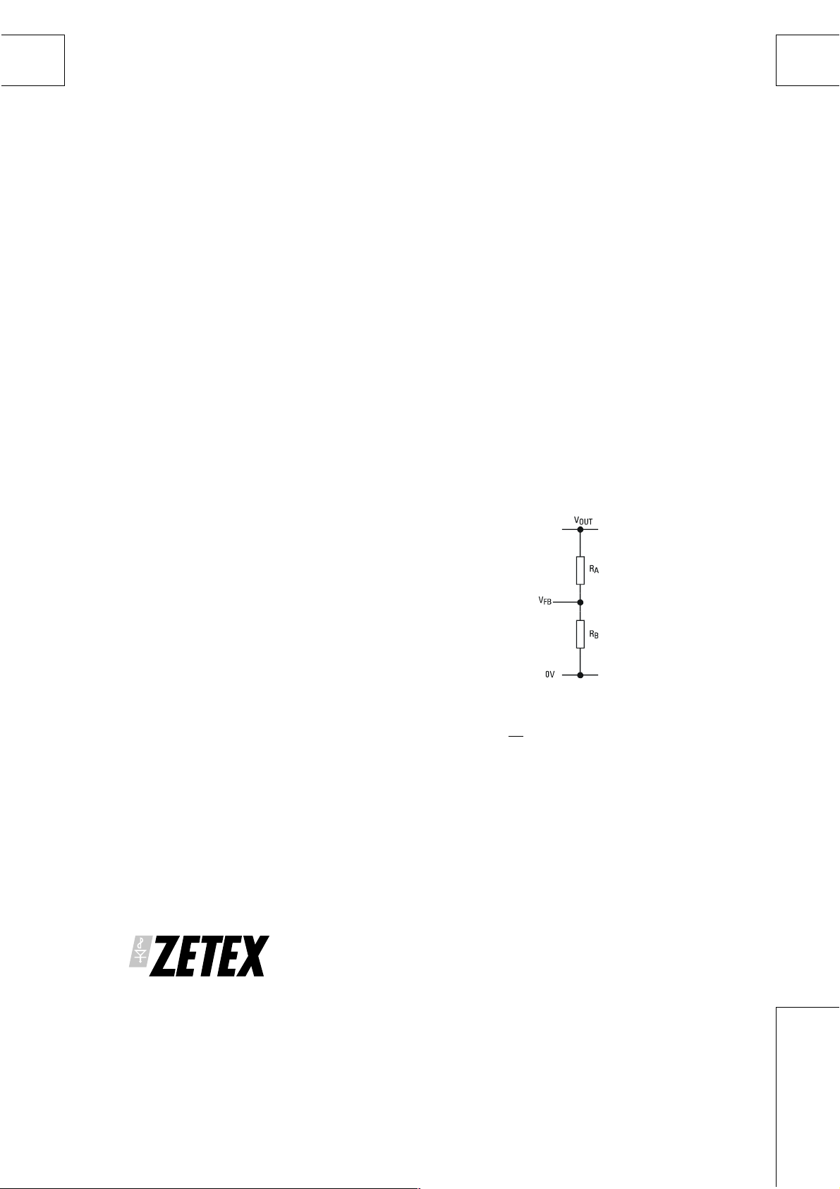
Output Voltage Adjustment
The ZXRD1000 is available as either a fixed 5V, 3.3V or
adjustable output. On fixed output versions, the V
should be connected to the o utput. Adjustable operation
requires a resistive divider connected as fo llows:
The value of the output voltage is determined by the
equation
R
V
OUT
= VFB (1 +
A
V
=1.24V
)
R
FB
B
Note: The adjustable circuit is shown in the following
transient optimisat ion sect ion. It is also used in t he
evaluation PCB. In both t hese circuit s R
the label R6 and R
the label R5.
B
A
Values of resist or should be between 1k and 20k to
guarantee operation. Output voltage can be adjusted in
the range 2V to 12V for non-synchronous ap plications.
For synchronous applications, the minimum V
by the V
MOSFET, as the swing in the gate using the
SimpleSync
threshold required for the synchronous
GS
TM
technique is approximately V
pin
FB
is assigned
is set
OUT
.
OUT
8
ISSUE 4 - OCTOBER 2000
Applications (continued)
ZXRD1000 SERIES
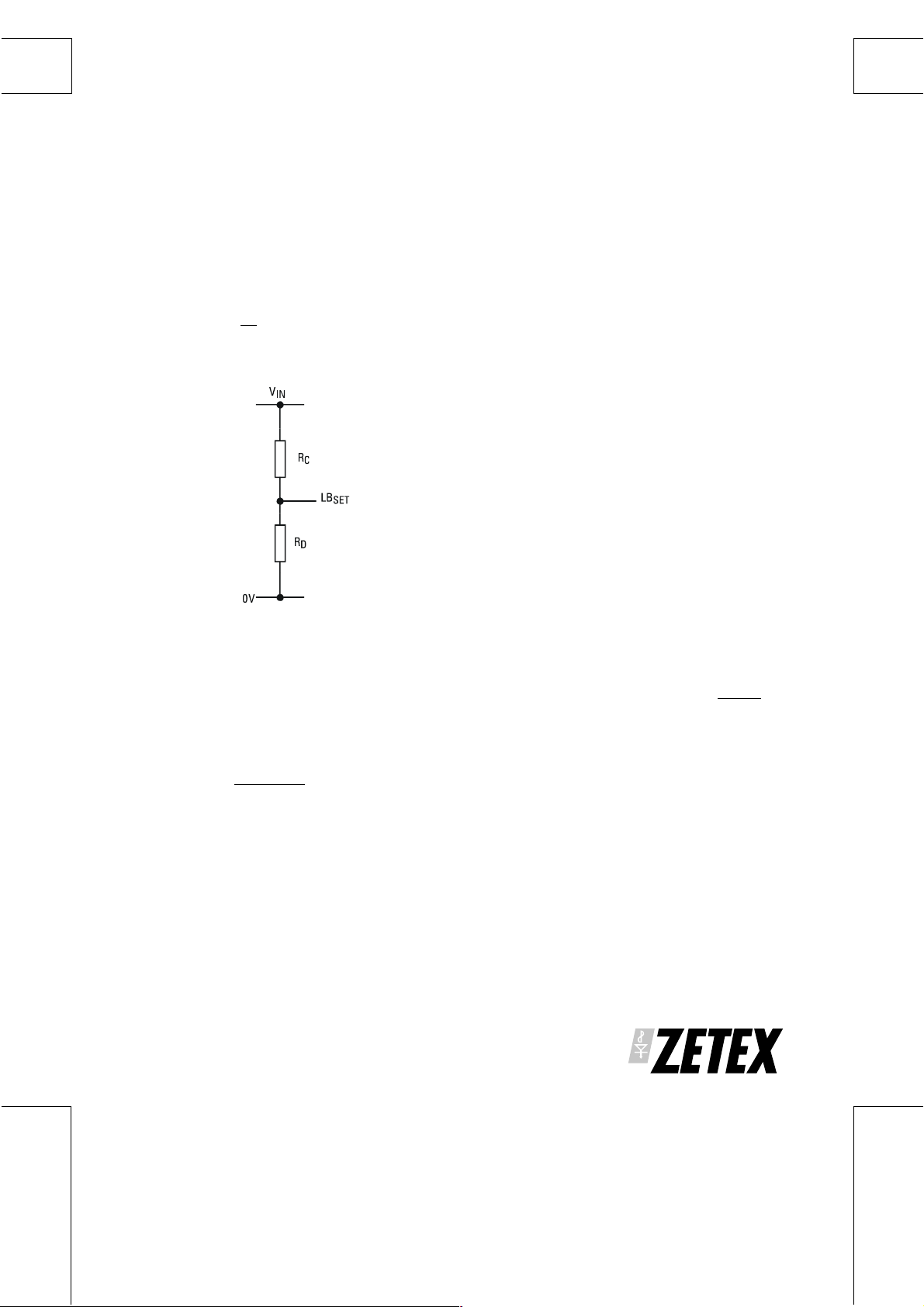
Low Battery Flag
The low battery flag threshold can be set by the user
to trip at a level determined by the equation:
R
V
LBSET
= 1.25
C
1 +
)
(
R
D
RD is recommended to be 10k where RC and RD are
connected as follows:
Hysteresis is typically 20mV at the LB
SET
pin.
Current Limit
A current limit is set by the low value resistor in the
output path, R
overload current limit, it does not need to be accurate
and can hence be a low cost device.
The value of the current limit is set by using the
equation:
I
LIM
(A) =
A graph of Current Limit v R
typical characteristics. This should assist in the
selection of R
If desired, R
When used on the input side R
with the upper output device (i.e. in series with the
drain or source in N and P channel solutions
respectively).Typically in this configuration R
be 20m⍀.
. Since the resistor is only used for
SENSE
50(mV)
R
(mΩ)
SENSE
is shown in the
SENSE
appropriate to application.
SENSE
can also be on the input supply side.
SENSE
should be in series
SENSE
SENSE
will
Hiccup Time Constant
The hiccup circuit (at the ’delay’ pin) provides overload
protection for the soluti on. The threshold of the hiccup
mode is determined by the value of R
SENSE,
When
>50mV is developed across the sense resistor, the
hiccup circuit is triggered, inhibiting the device.
It will stay in this state depending upon the time
constant of the resistor and capacitor connected at the
’delay’ pin. In order to keep the dissipation down
under overload conditions it is recommended the
circuit be off for approximately 100ms. If for other
application reasons this is too long an off period, this
can be reduced at least by 10:1, care needs to be taken
that any increased dissipation in the external MOSFET
is still acceptable. The resistor capacitor combination
R1,C1 recommended in the applications circuits
provides a delay of 100ms.
Soft Start & Loop Stability
Soft start is determined by the time constant of the
capacitor and resistor C7 and R3. Typically a good
starting point is C7 = 22µF and R3 = 24k for fixed
voltage variants. For fully adjustable variants see
Optimising for Transient Response later in the
applicati ons sec ti on . This net wor k al so he lps prov i de
good loop stability.
Low Quiescent Shutdown
Shutdown control is provided via the SHDN pin,
putting the device in to a low quiescent sleep mode.
In some circumstances where rapid sequencing of V
can occur (when VCC is turned off and back on) and V
has a very rapid rise time (100-200ms) timing conflicts
can occur.
CC
CC
ISSUE 4 - OCTOBER 2000
9

ZXRD1000 SERIES
Optimising for Transient Response.
Transient response is important in applications where
the load current increases and decreases rapidly. To
optimise the system for good transient response
certain criteria have to be observed.
The optimum solution using t he ZXRD seri es uses the
adjustable N phase controller in synchrono us mode as
represented in the diagram opposite. The external
networks for this solution require the use of the
adjustable controller option.
By using standar d ’bulk’ capacitors in parallel w ith a
single OS-CON capacitor significant performance
versus cost advantage can be given in this application.
The low ESR of the OS-CON capacitor provides
competitive output voltage ripple at low capacitance
values. The ’bulk’ capacitors aid transient response.
However, the low ESR of the OS-CON capacitor can
cause instability within the system. To maintain
stability an RC network (R
implemented. Furthermore, a capacitor in parallel with
R6 (C
2) is required to optimise transient respo nse. To
x
do this the appropriate adjustabl e ZXRD must be used
because the input to the internal error amplifier (pin
16) has to be accessed. The adjustable device differs
from fixed controller versions in this respect. This
combined with a frequency compensation ad justment
gives an optimised solution for excellent transient
response.
, Cx1) has to be
X
Layout Issues
Layout is critical for the circui t to fu ncti on in the most
efficient manner in terms of electrical efficiency,
thermal considerations and noise. The following
guidelines should be observed:
A 2.2µF (C8) decoupling capacitor should be as close
as possible to the drive MOSFETs and D1 anode. This
capacitor is effectively connected across V
but should be as close as possible to the appropriate
components in either N or P, synchronous or
non-synchronous configurations. Furthermore the
G
connection o f the sync hronou s MOSFET /D1 a nd
ND
output capacitors should be close together and use
either a ground plane or at the very least a low
inductance PCB track.
For the standard application circuits, a G erber file can
be made available for the layout which uses the
materials as listed in the bill of materials table for the
reference designs.
and G
IN
ND
Reference Designs.
In the following section reference circuit s are show n for
the ZXRD series in both synchronous and
non-synchronous modes. These are shown for each of
the N and P phase controllers. In each case efficiency
graphs are shown for the appropriate configuration
using 3.3V and 5V ZXRD devices. The BOM is then
shown for the design. Additional and alternative
components are shown with a ’*’. These refer to
modifications to the design to optimise for transient
response. Optimisation is reached using th e adjustable
version of either N or P ph ase controller device.
10
ISSUE 4 - OCTOBER 2000

D2
BAT54
OUT
V
L1
15µH
N1
ZXM64N02X
3.3V 4A
SENSE
R
C11
1µF
0.01R
Cx2
R6
10k
0.01µF
ZXRD1000 SERIES
C9
1µF
OUT
120µF
C
x2
680µF
R5
6k
2.2µF
C8
ZHCS1000
D1
Fx
N2
ZXM64N02X
D3
BAT54
converter 200kHz.
TM
CC
V
4.5-10V
ISSUE 4 - OCTOBER 2000
R4
10k
RX
1µF
8
14
SENSE -
R
Delay
10
16
FB
V
Comp
T
INT
Decoup
C
V
6
5
CX1
15
2k7
0.022µF
R2
680R
GNDPWR
ND
G
34
1µF
330pF
C2
C1
IN
C
C4
68µF
C7
22µF
R3
3k
C3
1µF
1µF
Op timised Transient Response, 4.5V-10V Input, 3V/4A Output, N Phase Adjustable, SimpleSync
1µF
C10
C6
2
1
7
DRIVE
V
IN
13
V
IC1
SHDN
9
R1
100k
Shut Down
Bootstrap
SET
LB
C5
1µF
SENSE+
R
LBF
11
Low input flag
11

ZXRD1000 SERIES
4.5V -10VInput, 3.3V/4A Output, N Phase, High Efficiency SimpleSyncTM Converter
200kHz
V
CC
4.5-10V
Shut Down
Low input flag
D2
N1
C11
Fx
R4
D3
N2
L1
C8
D1
R
SENSE
V
OUT
3.3V 4A
C9
C
OUT
SHDN
LB
SET
LBF
Delay
Decoup
V
INT
C
T
GNDG
R3
13
V
IN
V
DRIVE
Bootstrap
R
SENSE+
R
SENSE -
Comp
PWR
ND
34
C10
2
1
7
C6
8
16
V
F B
15
R2
C7
R1
C
IN
C1
IC1
9
C5
11
14
10
6
5
C3C2
C4
ZXRD1033NQ16
100
95
90
85
80
75
70
65
Efficiency (%)
60
55
50
0.1 1
I (A)
OUT
12
V =7V
IN
V =10V
IN
Efficiency v I
V =5.0V.
OUT
OUT
ZXRD1050NQ16
10
ISSUE 4 - OCTOBER 2000

ZXRD1000 SERIES
Ref Value Part Number Manufacturer Comments
IC1 ZXRD1033NQ16 Zetex QSOP16 Controller IC
N1
V
>7V
IN
<7V
V
IN
N2
D1 1A 0. 5V V
F
D2 10mA 0 .4V V
D3 10mA 0 .4V V
ZXM64N03X
ZXM64N02X
ZXM64N02X
ZHCS1000 Zetex SOT23 Schottky Diode 1A
BAT54 Zetex SOT23 Schottky Diode
F
BAT54 Zetex SOT23 Schottky Diode
F
Zetex MSOP8 Low R
N MOSFET 30V V
20V V
R1 100k WCR0805-100k Welwyn/IRC 0805 Size
R2 680⍀ WCR0805-680 Welwyn/IRC 0805 Size
R3 24k WCR0805-24k Welwyn/IRC 0805 Size
*R3 3k WCR0805-3k Welwyn/IRC 0805 Size
R4 10k WCR0805-10k Welwyn/IRC 0805 Size
*Rx 2.7K WCR0805-2.7k Welwyn/IRC 0805 Size
R
SENSE
C
IN
OR
OR
C
OUT
OR
OR
C
OUT
C1 1FGeneric
C2 1FGeneric
0.01⍀ LR1206R010 Welwyn/IRC Current Limit Sense Resistor
68F
68F
68F
470F
*150F
*120F
TPSD68M016R0150
20SA68M
20SV68M
TPSE477M010R0200
6SA150M
6SV120M
AVX
Sanyo OS-CON
Sanyo OS-CON
AVX
Sanyo OS-CON
Sanyo OS-CON
68F 16V ’E’ low ESR
68F 20V PTH low ESR
68F 20V SMT low ESR
470F 10V ’E’ low ESR
150F 6V PTH low ESR
120f 6V SMT low ESR
680F x 2 6CV680GX Sanyo 680F 6V SMT Bulk Capacitor
1µF,10V. X7R Diel ectric
1µF,4V.X 7R Dielec tric
C3 330pF Generic 330pF,4V.X7R Dielectric
C4 1FGeneric
C5 1FGeneric
C6 1FGeneric
C7 22FGeneric
C8 2.2FGeneric
C9 1FGeneric
C10 1 FGeneric
C11 1 FGeneric
*Cx1 0.022FGeneric
1µF,10V. X7R Diel ectric
1µF,10V. X7R Diel ectric
1µF,4V.X 7R Dielec tric
22µF,4V.X7R Dielectric
2.2µF,10V.X7R Dielectric
1µF,10V. X7R Diel ectric
1µF,10V. X7R Diel ectric
1µF,10V. X7R Diel ectric
0.022µF,4V.X7R Dielectric
*Cx2 10nF Generic 10nF,10V.X7R Dielectric
L1
OR
15H
10H
CDRH127B-OWZ9
6001
Sumida SMT
C&D Technologies
Low Profile SMT
Low Profile SMT
(NCL)
Fx 2785044447 FairRite SMT Ferrite Bead
* see Optimising for Transient Response Section
DS(ON)
20V V
DS
DS
DS
ISSUE 4 - OCTOBER 2000
13

ZXRD1000 SERIES
4.5V -10VInput, 3.3V/4A Output, N Phase, High Efficiency Non-Synchronous Step
Down Converter 200kHz
V
CC
4.5-10.0V
IC1
Shut Down
Low input flag
9
6
5
SHDN
LB
SET
LBF
Delay
Decoup
V
INT
C
T
V
Bootstrap
GNDG
R3
13
IN
PWR
34
V
R
SENSE+
R
SENSE -
Comp
ND
D2
C10
2
DRIVE
1
7
C6
8
16
V
F B
15
R2
D3
C7
C11
R4
R1
C5
C
IN
C1
11
14
10
C4
C3C2
100
95
V =5V
IN
90
V =10V
85
IN
80
75
Efficiency (%)
70
65
60
Efficiency v I
55
50
0.1 1 10
I (A)
OUT
100
V =7V
95
90
85
IN
V =10V
IN
80
Efficiency (%)
75
70
65
60
Efficiency v I
55
50
0.1 1 10
I(A)
OUT
C8
N1
L1
D1
OUT
V =3.3V.
OUT
V=5V.
OUT
OUT
R
SENSE
C
C
OUT
OUT
ZXRD1033NQ16
ZXRD1050NQ16
V
3.3V 4A
C9
OUT
14
ISSUE 4 - OCTOBER 2000

ZXRD1000 SERIES
Ref Value Part Number Manufacturer Comments
IC1 ZXRD1033NQ16 Zetex QSOP16 Controller IC
N1
V
>7V
IN
<7V
V
IN
D1 5A 0. 5V V
F
D2 10mA 0 .4V V
D3 10mA 0 .4V V
ZXM64N03X
ZXM64N02X
50WQ04FN Zetex Schottky Diode 5A
BAT54 Zetex SOT23 Schottky Diode
F
BAT54 Zetex SOT23 Schottky Diode
F
Zetex MSOP8 Low R
N MOSFET 30V V
20V V
R1 100k WCR0805-100k Welwyn/IRC 0805 Size
R2 680⍀ WCR0805-680 Welwyn/IRC 0805 Size
R3 24k WCR0805-24k Welwyn/IRC 0805 Size
*R3 3k WCR0805-3k Welwyn/IRC 0805 Size
R4 10k WCR0805-10k Welwyn/IRC 0805 Size
*Rx 2.7K WCR0805-2.7k Welwyn/IRC 0805 Size
R
SENSE
C
IN
OR
OR
C
OUT
OR
OR
C
OUT
C1 1FGeneric
C2 1FGeneric
0.01⍀ LR1206R010 Welwyn/IRC Current Limit Sense Resistor
68F
68F
68F
470F
*150F
*120F
TPSC68M02R0150
20SA68M
20SV68M
TPSE477M010R0200
6SA150M
6SV120M
AVX
Sanyo OS-CON
Sanyo OS-CON
AVX
Sanyo OS-CON
Sanyo OS-CON
68F 25V ’E’ low ESR
68F 20V PTH low ESR
68F 20V SMT low ESR
470F 10V ’E’ low ESR
150F 6V PTH low ESR
120f 6V SMT low ESR
680F x 2 6CV680GX Sanyo 680F 6V SMT Bulk Capacitor
1µF,10V. X7R Diel ectric
1µF,4V.X 7R Dielec tric
C3 330pF Generic 330pF,4V.X7R Dielectric
C4 1FGeneric
C5 1FGeneric
C6 1FGeneric
C7 22FGeneric
C8 2.2FGeneric
C9 1FGeneric
C10 1 FGeneric
C11 1 FGeneric
*Cx1 0.022FGeneric
1µF,10V. X7R Diel ectric
1µF,10V. X7R Diel ectric
1µF,4V.X 7R Dielec tric
22µF,4V.X7R Dielectric
2.2µF,10V.X7R Dielectric
1µF,10V. X7R Diel ectric
1µF,10V. X7R Diel ectric
1µF,10V. X7R Diel ectric
0.022µF,4V.X7R Dielectric
*Cx2 10nF Generic 10nF,10V.X7R Dielectric
L1
OR
15H
15H
CDRH127-150MC
DP5022P-153
Sumida
Coilcraft
Low Profile SMT
Low Profile SMT
* see Optimising for Transient Response Section
DS(ON)
DS
DS
ISSUE 4 - OCTOBER 2000
15

ZXRD1000 SERIES
5V -18V Input, 5V/3A Output, P Phase, High Efficiency SimpleSync
V
CC
5V-18V
IC1
Shut Down
Low input flag
R1
9
C5
C
IN
C1
11
14
10
6
5
C4
C3C2
100
95
90
85
80
75
Efficiency (%)
70
65
60
55
50
0.1 1
100
95
90
85
80
Efficiency (%)
75
70
65
60
55
50
0.1 1 10
SHDN
LB
SET
LBF
Delay
Decoup
V
INT
C
T
GNDG
R3
13
V
IN
V
DRIVE
Bootstrap
R
SENSE+
R
SENSE -
V
Comp
PWR
ND
34
2
1
7
C6
8
16
F B
15
R2
C7
V =5V
IN
V =12V
IN
Efficiency v I
I (A)
OUT
V =7V
IN
V =12V
IN
Efficiency v I
I(A)
OUT
P1
D1
Fx
N1 C8
OUT
V =3.3V.
OUT
V=5V.
OUT
OUT
TM
Converter 200kHz
L1
R
SENSE
ZXRD1033PQ16
10
ZXRD1050PQ16
V
OUT
5.0V 3A
C9
C
OUT
16
ISSUE 4 - OCTOBER 2000

ZXRD1000 SERIES
Ref Value Part Number Manufacturer Comments
IC1 ZXRD1050PQ16 Zetex QSOP16 Controller IC
P1
V
V
IN
IN
>12V
<12V
ZXM64P03X
ZXM64P02X
Zetex MSOP8 Low R
P MOSFET 3 0V V
20V VDS
N1 ZXM64 NO3 X Zetex MSOP8 Low R
D1 1A 0. 5V V
F
ZHCS1000 Zetex Schottky Diode 1A
R1 100k WCR0805-100k Welwyn/IRC 0805 Size
R2 680⍀ WCR0805-680 Welwyn/IRC 0805 Size
R3 24k WCR0805-24k Welwyn/IRC 0805 Size
*R3 3k WCR0805-3k Welwyn/IRC 0805 Size
*Rx 2.7K WCR0805-2.7k Welwyn/IRC 0805 Size
R
SENSE
C
IN
OR
OR
C
OUT
OR
OR
C
OUT
C1 1FGeneric
C2 1FGeneric
0.015⍀ LR1206R015 Welwyn/IRC Current Limit Sense Resistor
68F
68F
68F
470F
*150F
*120F
TPSV686M025R0150
20SA68M
20SV68M
TPSE477M010R0200
6SA150M
6SV120M
AVX
Sanyo OS-CON
Sanyo OS-CON
AVX
Sanyo OS-CON
Sanyo OS-CON
68F 25V ’E’ low ESR
68F 20V PTH low ESR
68F 20V SMT low ESR
470F 10V ’E’ low ESR
150F 6V PTH low ESR
120f 6V SMT low ESR
680F x 2 6CV680GX Sanyo 680F 6V SMT Bulk Capacitor
1µF,20V. X7R Diel ectric
1µF,4V.X 7R Dielec tric
C3 330pF Generic 330pF,4V.X7R Dielectric
C4 1FGeneric
C5 1FGeneric
C6 1FGeneric
C7 22FGeneric
C8 2.2FGeneric
C9 1FGeneric
*Cx1 0.022FGeneric
1µF,20V. X7R Diel ectric
1µF,20V. X7R Diel ectric
1µF,4V.X 7R Dielec tric
22µF,4V.X7R Dielectric
2.2µF,20V.X7R Dielectric
1µF,20V. X7R Diel ectric
0.022µF,4V.X7R Dielectric
*Cx2 10nF Generic 10nF,20V.X7R Dielectric
L1
OR
15H
10H
CDRH127B-OWZ9
6001
Sumida
C&D Technologies
Low Profile SMT
Low Profile SMT
(NCL)
Fx 2785044447 FairRite SMT Ferrite Bead
* see Optimising for Transient Response Section
DS(ON)
DS(ON)
MOSFET
DS
ISSUE 4 - OCTOBER 2000
17

ZXRD1000 SERIES
5V -18V Input, 5V/3A Output, P Phase, High Efficiency Non-synchronous Step Down
Converter 200kHz
V
CC
5.0-18V
Shut Down
Low input flag
IC1
SHDN
LB
SET
LBF
Delay
Decoup
V
INT
C
T
V
GNDG
R3
13
IN
V
DRIVE
Bootstrap
R
SENSE+
R
SENSE -
V
Comp
PWR
ND
34
2
1
7
C6
8
16
F B
15
R2
C7
R1
9
C5
C
IN
C1
11
14
10
6
5
C3C2
C4
C8
P1
L1
D1
R
SENSE
V
OUT
5.0V 3A
C9
C
OUT
100
95
90
85
V =5V
IN
V =12V
IN
80
75
Efficiency (%)
70
65
60
55
50
0.1 1 10
100
I (A)
OUT
95
90
85
Efficiency v I
V =3.3V.
V =7V
IN
V =12V
IN
OUT
OUT
ZXRD1033PQ16
80
Efficiency (%)
75
70
65
60
55
50
0.1 1 10
I (A)
OUT
Efficiency v I
V =5V.
OUT
OUT
ZXRD1050PQ16
18
ISSUE 4 - OCTOBER 2000

ZXRD1000 SERIES
Ref Value Part Number Manufacturer Comments
IC1 ZXRD1050PQ16 Zetex QSOP16 Controller IC
P1
V
>12V
IN
<12V
V
IN
D1 5A 0. 5V V
F
ZXM64P03X
ZXM64P02X
50WQ04FN IR Schottky Diode 5A
R1 100k WCR0805-100k Welwyn/IRC 0805 Size
R2 680⍀ WCR0805-680 Welwyn/IRC 0805 Size
R3 24k WCR0805-24k Welwyn/IRC 0805 Size
*R3 3k WCR0805-3k Welwyn/IRC 0805 Size
*Rx 2.7k WCR0805-2.7k Welwyn/IRC 0805 Size
R
SENSE
C
IN
OR
OR
C
OUT
OR
OR
C
OUT
0.015⍀ LR1206R015 Welwyn/IRC Current Limit Sense Resistor
68F
68F
68F
470F
*150F
*120F
TPSV686M025R0150
20SA68M
20SV68M
TPSE477M010R0200
6SA150M
6SV120M
680F x 2 6CV680GX Sanyo 680F 6V SMT Bulk Capacitor
C1 1FGeneric
C2 1FGeneric
C3 330pF Generic 330pF,4V.X7R Dielectric
C4 1FGeneric
C5 1FGeneric
C6 1FGeneric
C7 22FGeneric
C8 2.2FGeneric
C9 1FGeneric
*Cx1 0.022FGeneric
*Cx2 10nF Generic 10nF,20V.X7R Dielectric
L1 15H
15H
CDRH127-150MC
D05022P-153
* see Optimising for Transient Response Section
Zetex MSOP8 Low R
P MOSFET 3 0V V
20V VDS
AVX
Sanyo OS-CON
Sanyo OS-CON
AVX
Sanyo OS-CON
Sanyo OS-CON
68F 25V ’E’ low ESR
68F 20V PTH low ESR
68F 20V SMT low ESR
470F 10V ’E’ low ESR
150F 6V PTH low ESR
120f 6V SMT low ESR
1µF,20V. X7R Diel ectric
1µF,4V.X 7R Dielec tric
1µF,20V. X7R Diel ectric
1µF,20V. X7R Diel ectric
1µF,4V.X 7R Dielec tric
22µF,4V.X7R Dielectric
2.2µF,20V.X7R Dielectric
1µF,20V. X7R Diel ectric
0.022µF,4V.X7R Dielectric
Sumida SMT
Coilcraft
Low Profile SMT
Low Profile SMT
DS(ON)
DS
ISSUE 4 - OCTOBER 2000
19

ZXRD1000 SERIES
Designing with the ZXRD and Dynamic
Performance
This section refers to the reference design for the 3.3V,
4A output N channel synchronous converter. This is
as shown previously in the Optimising for transient
response section of the applications i nformation (page
10). This circuit is also representative of the ZXRD
evaluation board (see ordering information).
The ZXRD series has been designed to give the best
in terms of all round flexibility allowing engineers to
either use the reference design as is, or to tailor the
design to the individual requirements. This section
demonstrates the performance features of the ZXRD
series and its associated components.
Efficiency
Efficiency is often quoted as one of the key parameters
of a DC-DC converter. Not only does it give an
instantaneous idea of heat dissipation, but also an idea
as to the extent battery life can be extended in say
portable applications. Fig.1 shows th e efficiency of the
standard application circuit. Efficiency vs Output
current is shown for the 5 to 3.3V configuration.
100
95
90
85
80
Efficiency (%)
75
70
65
60
55
50
0.1 1 10
Startup
Startup is always important in DC-DC converter
applications. Magnetics have large inrush current
requirements. For higher current applications using
large input and output capacitors the startup current can
be quite significant. This can cau se several problems.
In many applications the power supply to the DC-DC
converter can be affected. Particularly in battery
powered applications, trying to take large steps in
load current out of the supply can result in either
current limitation (by the internal impedance of the
battery), or it can actually damage the battery.
For the converter itself, large changes in load current
can result in false triggering of the RSENSE circuit. This
could result in device hiccup (see applications section).
The ZXRD programmable soft start function
eliminates both these problems. This is very clear to
see in operation if the main switching waveforms are
examined.
The soft start is programmed by the combination of
resistor and capacitor R3 and C7. As a recommendation,
R3 and C7 are set to 3k and 22µF respectively, which limits
the peak startup current appropriately in the reference
circuit. Fig.2 shows the startup waveforms. V
are plotted against time
V =5V
IN
I (A)
OUT
Efficiency v I
V =3.3V.
OUT
OUT
and V
IN
OUT
Fig.1. 5-3.3V Efficiency to 4A
20
ISSUE 4 - OCTOBER 2000

Fig.2. Startup Waveform for 3.3V output .
SimpleSyncTM and Shoot-Through
Steady state operation under constant load gives
an excellent indication of the ZXRD series
performance and also demonstrates how well
SimpleSync
technique dr ives the synch ronous MOSFET gate
using the overwinding on the main inductor. It
also uses the high speed suppression characteristics
of the ferrite bead to prevent shoot through
currents. Fig.3 shows the gate waveforms for the
main and synchronous MOSFET devices (Zetex
ZXM64N02X).
TM
works. The SimpleSync
TM
ZXRD1000 SERIES
Output Voltage Ripple
Output voltage ripple is shown in Fig.4 and Fig. 5
for load currents of 0.5A and 4A respectively.
Output voltage ripple will be depen dant, to a very
large extent, on the output capacitor ESR. (see
Applications Se c t io n f or ripple calculation).
Fig.4 0.5A Main & V
Waveforms
OUT
Fig3. Main & Synchronous gate waveforms
ISSUE 4 - OCTOBER 2000
Fig.5 4A Main & V
21
Waveforms
OUT

ZXRD1000 SERIES
Line regulation
Variation in input voltage for both these conditions
(0.5A and 4A output) shows the excellent line
regulation the ZXRD. Fig.6 shows that with 0.5A and
4A output currents, applying an increase in input
voltage from 5V to 10V , results in only small ch anges
in output regulation.
Fig.6a Line Regulation 0.5A load
Fig.6b Line Regulation 4A load
Transient Response
Transient response to changes in load is becoming an
increasingly critical feature of many converter circuits.
Many high speed processors make very large step
changes in their load requirements, at the same time
as having more stringent specifications in terms of
overshoot and undershoot. Fig.7 demonstrates the
excellent load transient performance of the ZXRD
series. A step change using an electronic load from 1A
to 3A is sho wn wit h corre spondin g output t ransie nt
performance.
Fig.7 Output Transient Response
Non-synchronous Applications
One of the key features of the ZXRD series, when
combined with the SimpleSync
flexibility in allowing engineers to choose either a
synchronous or non-synchronous architecture.
Making the design non-synchronous by removing
MOSFET N2 (the synchronous device), replacing the
ZHCS1000 with a high current diode (50WQ04FN)
and using a 2 terminal inductor, such as the Sumida
CDRH127-150MC, decreases cost slightly at the
expense of a few efficiency points. Fig.8 shows the
effect on the efficiency of the 5 to 3.3V 4A application
when the design is made non-s y n c hronous.
22
TM
technique , i s t he
ISSUE 4 - OCTOBER 2000

100
95
90
85
80
75
Efficiency (%)
70
65
60
55
50
0.1 1 10
Fig.8 Efficiency for non-synchronous 5-3.3V conversion
Using ’P’ Channel Devices (No Boot strap)
All the preceeding examples utilise N channel
MOSFET devices and a boots trap circuit to provi de full
enhancement to the high side device. These circuits
have a maximum input voltage of 10V. For
applications requiring a higher input voltage, using P
channel devices for the main MOS FET will allow u p to
18V operation. Typically this may be in a 12V to 5V
converter circuit.
ZXRD1000 SERIES
V =5V
IN
Efficiency v I
V =3.3V.
OUT
I(A)
OUT
If the same package size MOSFET devices are used, it
is likely a higher on resistance will be encountered,
with the result that efficiency will decline slightly.
Fig 9 shows the efficiency plot for a P phase
synchronous 5V converter based on the
ZXRD1050PQ16. The figure charts efficiency v output
current at 12V input and 7V input.
OUT
100
95
90
85
80
Efficiency (%)
75
70
65
60
55
50
0.1 1 10
Fig.9 ’P’ Channel Device Efficiency (synchronous)
ISSUE 4 - OCTOBER 2000
I (A)
OUT
23
V =7V
IN
V =12V
IN
Efficiency v I
V =5V.
OUT
OUT

ZXRD1000 SERIES
ZXCM6 Series
Low voltage MOSFETs
Unique structure gives optimum performance for switching applications.
N channel devices offer high efficiency
performance for switching applications.
This family of MOSFETs from Zetex offers a
combination of low on-resistance and low gate charge,
providing optimum performance and high efficiency
for switching applications such as DC - DC conversion.
On resistance is low across the family, from only 40mΩ
(max) for the ZXM64N02X part up to 180mΩ (max) for
the ZXM61N02F. This means that on-state losses are
minimised, impro ving efficiency in low fr equency drive
applications. Threshold voltages of 0.7V and 1V
minimum allow the MOSFETs to be driven from low
voltage sources.
To minimise switching losses, and hence increase the
efficiency of high frequency operation, gate charge (Qg )
is small. The maximum Qg varies from 3.4nC to 16nC
depending on which device is chosen. C
capacitance) is also low, e.g. typically 30pF for the
ZXM6203E6 device. This results in better efficiency in
high frequency applications.
rss
(Miller
P channel MOSFETs excel in load
switching applications.
The P-channel MOSFETs offer highly efficient
performance for low voltage load switching
applications. This helps increase battery life in portable
equipment.
Minimum threshold voltage is low, only 0.7V or 1V,
enabling the MOSFETs to provide optimum
performance from a low voltage so urce. To en sure th e
device suitability for low voltage applications, drain to
source voltage is specified at 20V or 30V.
To minimise on-sta te loss es, and im prove effici ency in
in low frequency drive applications, the on-resistance
(R
) is low across the range. For example, the
DS(ON)
ZXM64P03X has an R
source voltage of 4.5V.
Gate source charge is also low, easing requirem ents for
the gate driver. Maximum values range from 0.62nC for
the ZXM61P03F, up to 9nC for the ZXM64P03X.
of only 100mΩ at a gate to
DS(ON)
Small outline surface mount packaging
The products have been designed to optimise the
performance of a range of packages. The parts are
offered in SOT23, SOT23-6 and MSOP8 packages. The
MSOP8 enables single or dual devices to be offered.
The MSOP8 is also half the size of competitive SO8
devices and 20% smaller than TSSOP8 alternatives.
Product performance
The following performance characteristics show the
capabilities of the ZXM64N02X. This device is
recommended f or use with certain config urations of
the ZXRD DCDC controller circuit.
24
ISSUE 4 - OCTOBER 2000

Performance Characterisation of ZXM64N02X
ZXRD1000 SERIES
ELECTRICAL CHARACTERISTICS (at T
= 25°C unless otherwise stated).
amb
PARAMETER SYMBOL MIN. TYP. MAX. UNIT CONDITIONS.
STATIC
Drain-Source Breakdown Voltage V
Zero Gate Voltage Drain Current I
Gate-Body Leakage I
Gate-Source Threshold Voltage V
Static Drain-Source On-State
Resistance (1)
Forward Transconductance (3) g
(BR)DSS
DSS
GSS
GS(th)
R
DS(on)
fs
20 V
1
100 nA
0.7 V
0.040
0.050
µA
Ω
Ω
=250µA, VGS=0V
I
D
VDS=20V, VGS=0V
V
=± 12V,
GS
=0V
V
DS
=250µA, VDS=
I
D
V
GS
VGS=4.5V, ID=3.8A
=2.7V, ID=1.9A
V
GS
6.1 S VDS=10V,ID=1.9A
DYNAMIC (3)
Input Capacitance C
Output Capacitance C
Reverse Transfer Capacitance C
iss
oss
rss
1100 pF
350 pF
100 pF
=15 V,
V
DS
=0V, f=1MHz
V
GS
SWITCHING(2) (3)
Turn-On Delay Time t
Rise Time t
Turn-Off Delay Time t
Fall Time t
Total Gate Charge Q
Gate-Source Charge Q
Gate Drain Charge Q
d(on)
r
d(off)
f
g
gs
gd
5.7 ns
9.6 ns
28.3 ns
11.6 ns
16 nC
3.5 nC
5.4 nC
V
=10V, ID=3.8A
DD
R
=6.2Ω, RD=2.6Ω
G
(Refer to test
circuit)
=16V,VGS=4.5V
V
DS
=3.8A
, I
D
(Refer to test
circuit)
SOURCE-DRAIN DIODE
Diode Forward Voltage (1) V
Reverse Re cove ry Ti me (3) t
Reverse Re cove ry Cha rge( 3) Q
(1) Measured under pulsed conditions. Width=300µs. Duty cycle ≤2% .
(2) Switching characteristics are independent of operating junction temperature.
(3) For design aid only, not subject to production testing.
ISSUE 4 - OCTOBER 2000
SD
rr
rr
23.7 ns Tj=25°C, IF=3.8A,
13.3 nC
25
0.95 V Tj=25°C, IS=3.8A,
=0V
V
GS
di/dt= 100A/µs

ZXRD1000 SERIES
208221 b8066
GERMANY ASIA USA UK
Zetex
Sumida
FairRite
AVX
Welwyn, IR C
Coilcraft
Sanyo Electron ic
Comp. (OS-CON)
C & D Technologies
(NCL)
Zetex GmbH
Munich
(49) 894549490 (852) 2610 0611 (1) 631 543 7100 (44) 161 622 4444
http://www.zetex.com
http://www.japanlink.com/sumida/
Schaffner
Electronik GmbH
(49) 72156910
http://www.avxcorp.com
Welwyn
Electronics GmbH
(49)871 97376 0
http://welwyn-tt.co.uk
http://www.coilcraft.com
Sanyo Europe
Munich
(49) 89 457693 16
http://www.sanyovideo.com
Contact
C & D
Technologies
(NCL)
UK
Zetex Asia
Hong Kong
Sumida Electric
HK
(852) 2880 6688
Taiwan Sumida
Electric
(886) 2762 2177
Fair Rite Asia Pte
Ltd Singapore
(65) 281 1969
Japan/Korea
(81) 33225505 5
AVX Asia
Singapore
(65) 258 2833
TTC Group plc
Singapore
(65) 536 51667
SANYO
Electronics Ltd.
Hong Kong
(852) 21936888
Singapore
(65) 281 3226
Japan
(81) 720 70 630 6
C & D
Technologies
Guangzhou,
Guangdong, PRC
(86) 208221 80 66
Zetex Inc
Long Island NY
Sumida Electric
USA (CHICAGO
Head Office)
(1) 847 956-0666 (44) 1525 290755
FairRite Products
Corp
(1) 914 895 2055
AVX USA
(1) 843 448 9411
IRC Inc
(1) 512 992 7900
Coilcraft Inc
(1) 847 639 6400
SANYO
Electronics Ltd.
Forrest City, AR
870 633 5030
San Diego, CA
619 661 6835
Rochelle Pk, NJ
201 843 8100
C & D
Technologies
(NCL)
5816 Creedmoor
Road,
Raleigh
North Carolina
27612
(1) 919 571 9405
Zetex PLC
Chadderton,
Oldham
Ole Wolf
Electronics Ltd.
Schaffner EMC Ltd
(44) 118 977 0070
AVX UK
(44) 1252 770000
Welwyn
Components Ltd
(44) 1670 822181
Coilcraft Europe
(44) 1236 730595
Semicon UK Ltd
(44) 1279 422224
C & D
Technologies
(NCL)
Tanners Drive
Blakelands North
Milton Keynes
MK14 5BU
(44) 1908 615232
http://www.dc-dc.com
26
ISSUE 4 - OCTOBER 2000

Connection Diagram
ZXRD1000 SERIES
Bootstrap
V
DRIVE
PWRG
G
ND
C
T
V
INT
R
SENSE +
R
SENSE -
ND
1
16
2
15
14
3
13
4
12
5
6
10
7
8
Package Dimensions
IDENTIFICA TION
RECESS
FOR PIN 1
V
FB
Comp
Delay
V
IN
LB
11
LBF
Note:
Connection diagram is the same for N and P Phase, adjustable and
fixed controllers. The V
pin has a different function between
FB
adjustable and fixed versions.
SET
Decoup
9
J
SHDN
A
B
C
E
PIN No.1
F
G
D
K
DIM Millimetres Inches
MIN MAX MIN MAX
A 4.80 4.98 0.189 0.196
B 0.635 0.025 NOM
C 0.177 0.267 0.007 0.011
D 0.20 0.30 0.008 0.012
E 3.81 3.99 0.15 0.157
F 1.35 1.75 0.053 0.069
G 0.10 0.25 0.004 0.01
J 5.79 6.20 0.228 0.244
K0° 8° 0° 8°
ISSUE 4 - OCTOBER 2000
27

ZXRD1000 SERIES
Ordering Information
Device Description T&R Suffix Partmarking
ZXRD1033NQ16 3.3 V Fixed controller N main switch TA , TC ZXRD1033 N
ZXRD1050NQ16 5.0 V Fixed controller N main switch TA , TC ZXRD1050 N
ZXRD100ANQ16 Adjustable controller N main switch TA, TC ZXRD100AN
ZXRD1033PQ16 3.3V Fixed controller P main switch TA, TC ZXRD1033P
ZXRD1050PQ16 5.0V Fixed controller P main switch TA, TC ZXRD1050P
ZXRD100APQ16 Adjustable controller P main switch TA, TC ZXRD100AP
’N main switch’ indicates controller for use with N channel main switch element.
’P main switch’ indicates controller for use with P channel main switch element.
TA= Tape and Reel quantity of 500
TC= Tape and Reel quantity of 2500
Demonstration Boards
These can be requested through your local Zetex office or representative. These bo ard s can be tailored to your
specific needs. If you would like to obtain a demo board then a request form is available to hel p determine your
exact requirement.
Zetex plc.
Fields New Road, Chadderton, Oldham, OL9-8NP, United Kingdom.
Telephone: (44)161 622 4422 (Sales), (44)161 622 4444 (General Enquiries)
Fax: (44)161 622 4420
Zetex GmbH Zetex Inc. Zetex (Asia) Ltd. These are supported by
Streitfeldstraße 19 4 7 Mall Drive, Unit 4 3701-04 Metroplaza, Tower 1 agents and distributors in
D-81673 Münc hen Commack NY 11725 Hing Fong Road, major countries world-wide
Germany USA Kwai Fong, Hong Kon g Zetex plc 2001
Telefon: (49) 89 45 49 49 0 Telephone: (631) 543-7100 Telephone:(852) 26100 611
Fax: (49) 89 45 49 49 49 Fax: (631) 864-7630 Fax: (852) 24250 494 http://www.zetex.com
This publication is issued to provide outline information only which (unless agreed by the Company in writing) may not be used, applied or reproduced for any
purpose or form part of any order or contract or be re garded as a represen ta tio n re l at ing to th e pr od uct s or serv ices con cer ne d . The Company reserves the
right to alter without notice the specification, design, price or conditions of supply of any product or service.
28
ISSUE 4 - OCTOBER 2000
 Loading...