ZETEX ZXMHC3A07T8 Technical data

查询ZXMHC10A07T8供应商
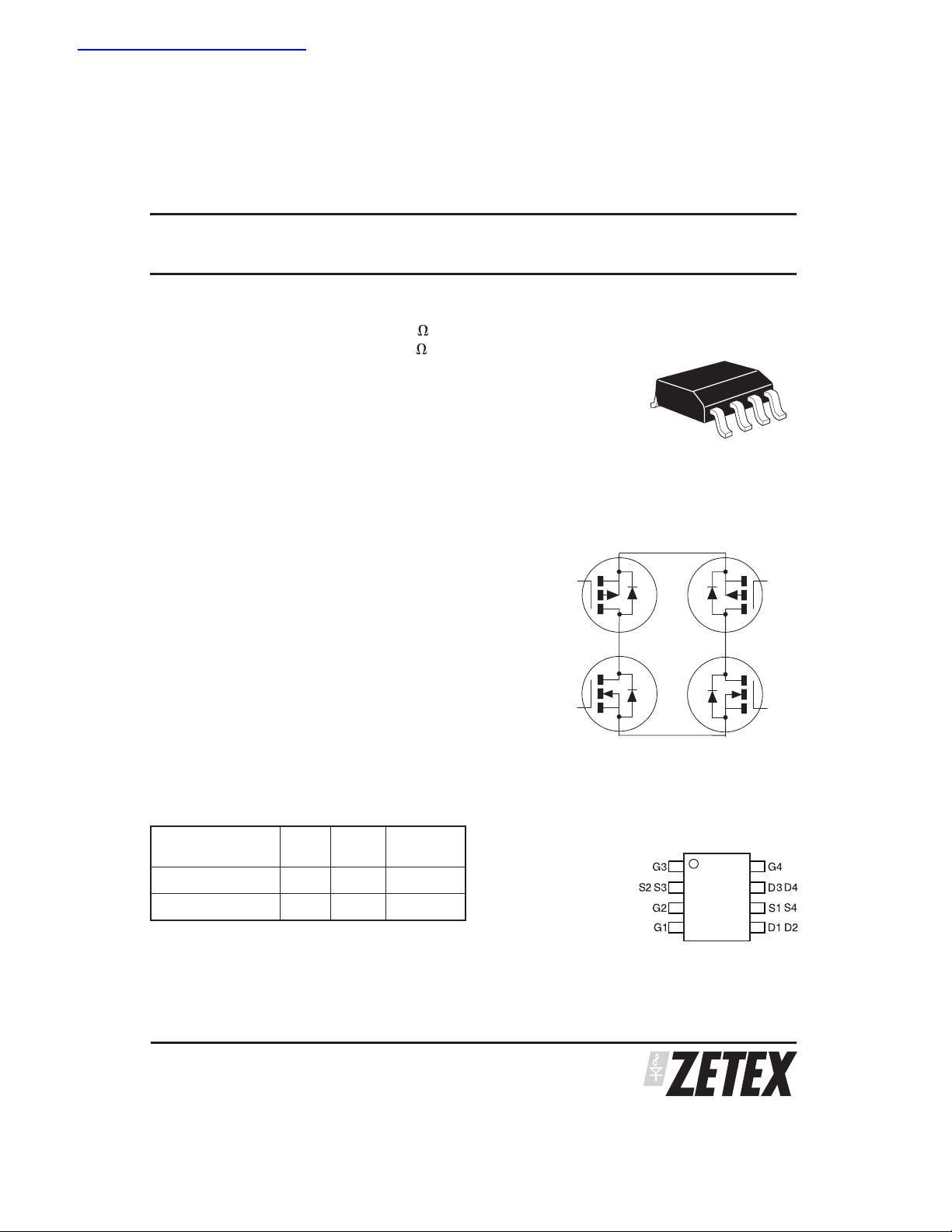
COMPLEMENTARY 100V ENHANCEMENT MODE MOSFET H-BRIDGE
SUMMARY
ZXMHC10A07T8
N-Channel = V
P-Channel = V
(BR)DSS
(BR)DSS
= 100V : R
= -100V : R
= 0.7 ; ID= 1.4A
DS(on)
= 1.0 ; ID= -1.3A
DS(on)
DESCRIPTION
This newgeneration of trench MOSFETs from Zetex utilizes a unique structure that
combines the benefits of low on-resistance with fast switching speed. This makes
them ideal for high efficiency, low voltage, power management applications.
FEATURES
Low on-resistance
•
G
Fast switching speed
•
1
• Low threshold
•
Low gate drive
•
Single SM-8 Surface Mount Package
APPLICATIONS
•
Single Phase DC Fan Motor Drive
D,1D
G
2
M
8
S
S
1
2
S
2
S
S
4
D,3D
3
G
4
4
G
3
ORDERING INFORMATION
DEVICE REEL
SIZE
ZXMHC10A07T8TA 7” 12mm 1000 units
ZXMHC10A07T8TC 13” 12mm 4000 units
TAPE
WIDTH
QUANTITY
PER REEL
DEVICE MARKING
•
ZXMH
C10A7
ISSUE 2 - JUNE 2005
PINOUT
1
SEMICONDUCTORS

ZXMHC10A07T8
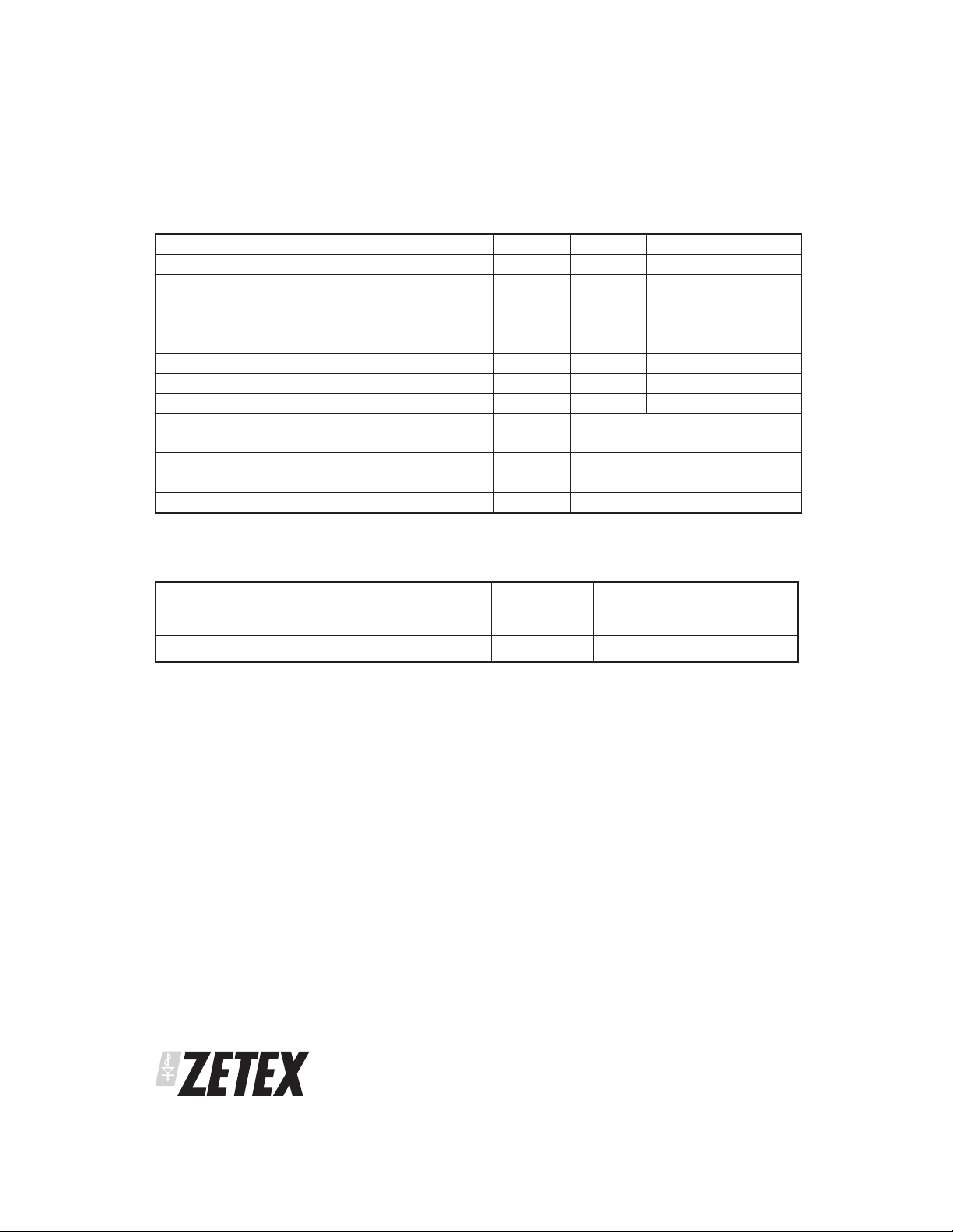
ABSOLUTE MAXIMUM RATINGS
PARAMETER SYMBOL N-channel P-channel UNIT
Drain-Source Voltage V
Gate-Source Voltage V
Continuous Drain Current
@V
GS
=10V; TA=25°C
@VGS=10V; TA=70°C
@VGS=10V; TA=25°C
Pulsed Drain Current
(c)
Continuous Source Current (Body Diode)
Pulsed Source Current (Body Diode)
Power Dissipation at T
=25°C
A
(c)
(a) (d)
(b) (d)
(b) (d)
(a) (d)
(b)
I
I
I
I
P
DSS
GS
D
DM
S
SM
D
Linear Derating Factor
Power Dissipation at T
=25°C
A
(b) (d)
P
D
Linear Derating Factor
Operating and Storage Temperature Range T
j,Tstg
THERMAL RESISTANCE
PARAMETER SYMBOL VALUE UNIT
Junction to Ambient
Junction to Ambient
NOTES
(a) For a device surface mounted on 50mm x 50mm x 1.6mm FR4 PCB with high coverage of single sided 2oz copper, in still air conditions, with
the heat sink split into two equal areas one for each drain connection.
(b) For a device surface mounted on FR4 PCB measured at t ⱕ 10 sec.
(c) Repetitive rating on 50mm x 50mm x 1.6mm FR4 PCB, D= 0.02, pulse width = 300s - pulse width limited by maximum junction temperature.
Refer to transiennt thermal impedance graph.
(d) For device with one active die.
(a) (d)
(b) (d)
R
R
⍜JA
⍜JA
100 -100 V
⫾20 ⫾20 V
1.1
0.9
1.0
-0.9
-0.8
-0.8
5.2 -4.5 A
2.3 -2.2 A
5.2 -4.5 A
1.3
10.4
mW/°C
1.3
10.4
mW/°C
-55 to +150 °C
94.5 °C/W
73.3 °C/W
A
A
A
W
W
SEMICONDUCTORS
ISSUE 2 - JUNE 2005
2

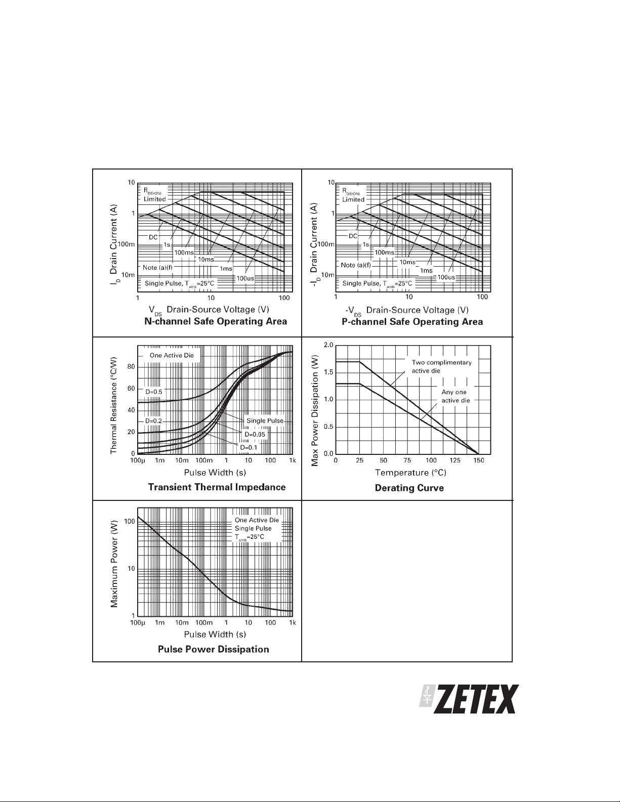
TYPICAL CHARACTERISTICS
ZXMHC10A07T8
ISSUE 2 - JUNE 2005
3
SEMICONDUCTORS
 Loading...