

查询ZXMC3AM832供应商
MPPS™ Miniature Package Power Solutions
COMPLEMENTARY 30V ENHANCEMENT MODE MOSFET
SUMMARY
N-Channel V
P-Channel V
DESCRIPTION
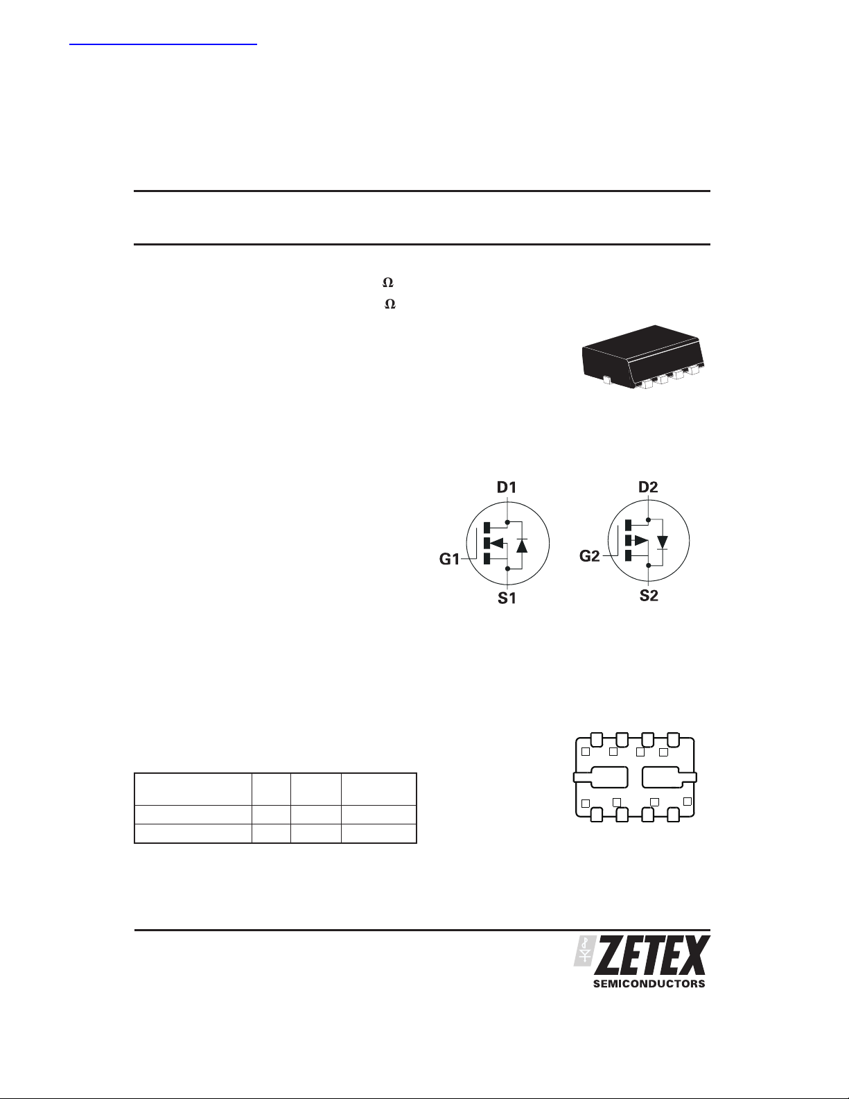
Packaged in the new innovative 3mm x 2mm MLP(Micro Leaded Package)
outline this dual 30V N channel Trench MOSFET utilizes a unique structure
combining the benefits of Low on-resistance with fast switching speed. This
makes them ideal for high efficiency, low voltage power management
applications. Users will also gain several other key benefits:
(BR)DSS
(BR)DSS
Performance capability equivalent to much larger packages
Improved circuit efficiency & power levels
PCB area and device placement savings
Reduced component count
= 30V; R
= -30V; R
= 0.12 ;ID= 3.7A
DS(ON)
= 0.21 ;ID= -2.7A
DS(ON)
ZXMC3AM832
3mm x 2mm Dual Die MLP
FEATURES
• Low on - resistance
•
Fast switching speed
•
Low threshold
•
Low gate drive
•
3mm x 2mm MLP
APPLICATIONS
•
MOSFET gate drive
•
LCD backlight inverters
•
Motor control
ORDERING INFORMATION
DEVICE REEL TAPE
ZXMC3AM832TA 7
ZXMC3AM832TC 13’‘ 8mm 10000 units
WIDTH
’‘ 8mm 3000 units
QUANTITY
PER REEL
DEVICE MARKING
C01
PINOUT
D2
G2
underside view
5
678
D2
S2
4
3 x 2 Dual MLP
D1
D1
S1
G1
1
23
PROVISIONAL ISSUE E - JULY 2004
1
ZXMC3AM832
ABSOLUTE MAXIMUM RATINGS
PARAMETER SYMBOL N-Channel P-Channel UNIT
Drain-Source Voltage V
Gate-Source Voltage V
Continuous Drain Current@V
@VGS=10V; TA=25⬚C
@VGS=10V; TA=25⬚C
=10V; TA=25⬚C
GS
(b)(f)
(b)(f)
(a)(f)
Pulsed Drain Current I
Continuous Source Current (Body Diode)
(b)(f)
Pulsed Source Current (Body Diode) I
Power Dissipation at TA=25°C
(a)(f)
I
I
P
DSS
GS
D
DM
S
SM
D
Linear Derating Factor
Power Dissipation at TA=25°C
(b)(f)
P
D
Linear Derating Factor
Power Dissipation at TA=25°C
(c)(f)
P
D
Linear Derating Factor
Power Dissipation at TA=25°C
(d)(f)
P
D
Linear Derating Factor
Power Dissipation at TA=25°C
(d)(g)
P
D
Linear Derating Factor
THERMAL RESISTANCE
PARAMETER SYMBOL VALUE UNIT
Junction to Ambient
Junction to Ambient
Junction to Ambient
Junction to Ambient
Junction to Ambient
Junction to Ambient
Notes
(a) For a dual device surface mounted on 8 sq cm single sided 2oz copper on FR4 PCB, in still air conditions with all exposed pads attached. The
copper are is split down the centre line into two separate areas with one half connected to each half of the dual device.
(b) Measured at t<5 secs for a dual device surface mounted on 8 sq cm single sided 2oz copper on FR4 PCB, in still air conditions with all exposed
pads attached. The copper are is split down the centre line into two separate areas with one half connected to each half of the dual device.
(c) For a dual device surface mounted on 8 sq cm single sided 2oz copper on FR4 PCB, in still air conditions with minimal lead connections only.
(d) For a dual device surface mounted on 10 sq cm single sided 1oz copper on FR4 PCB, in still air conditions with all exposed pads attached
attached. The copper are is split down the centre line into two separate areas with one half connected to each half of the dual device.
(e) For a dual device surface mounted on 85 sq cm single sided 2oz copper on FR4 PCB, in still air conditions with all exposed pads attached
attached. The copper are is split down the centre line into two separate areas with one half connected to each half of the dual device.
(f) For a dual device with one active die.
(g) For dual device with 2 active die running at equal power.
(h) Repetitive rating - pulse width limited by max junction temperature. Refer to Transient Thermal Impedance graph.
(i) The minimum copper dimensions required for mounting are no smaller than the exposed metal pads on the base if the device as shown in the
package dimensions data. The thermal resistance for a dual device mounted on 1.5mm thick FR4 board using minimum copper 1 oz weight, 1mm
wide tracks and one half of the device active is Rth = 250°C/W giving a power rating of Ptot = 500mW.
(a)(f)
(b)(f)
(c)(f)
(d)(f)
(d)(g)
(e)(g)
R
θJA
R
θJA
R
θJA
R
θJA
R
θJA
R
θJA
30 -30 V
⫾20 ⫾20 V
3.7
3.0
2.9
-2.7
-2.2
-2.1
12.4 -9.2 A
2.4 -2.8 A
12.4 -9.2 A
1.5
12
mW/°C
2.45
19.6
mW/°C
1
8
mW/°C
1.13
8
mW/°C
1.7
13.6
mW/°C
83.3 °C/W
51 °C/W
125 °C/W
111 °C/W
73.5 °C/W
41.7 °C/W
A
A
W
W
W
W
W
PROVISIONAL ISSUE E - JULY 2004
2
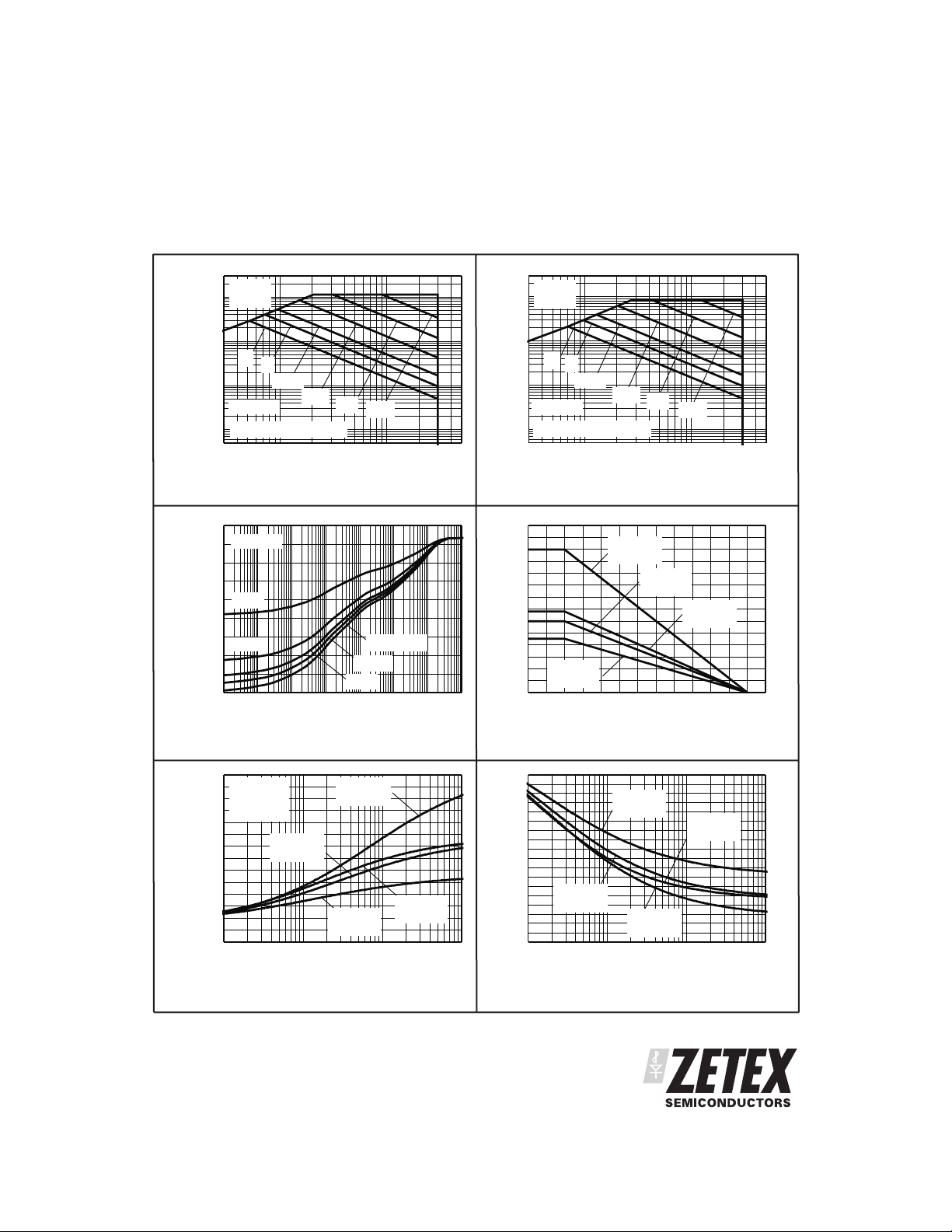
TYPICAL CHARACTERISTICS
ZXMC3AM832
R
DS(ON)
10
Limited
1
DC
1s
100m
D rainC urre n t (A )
D
I
10m
100ms
No te(a)(f)
Single Pulse, T
10ms
=25°C
amb
1ms
100us
110
VDSDrain-Source Voltage (V)
N-channel Safe Operating Area
No te(a)(f)
80
60
D=0.5
40
D=0.2
20
Therm al Resistance (°C/W)
0
100µ 1m 10m 100m 1 10 100 1k
Single Pulse
D=0.05
D=0.1
Pulse Width (s)
Transient Thermal Impedance
R
DS(ON)
10
Limited
1
DC
1s
100m
D rainC urre n t (A )
D
10m
-I
100ms
No te(a)(f)
Single Pulse, T
amb
10ms
=25°C
1ms
100us
110
-VDSDrain-Source Voltage (V)
P-channel Safe Operating Area
3.5
3.0
2.5
2.0
2oz Cu
No te(e)(g)
2oz Cu
No te(a)(f)
1.5
1.0
1oz Cu
0.5
No te(d)(f)
0.0
0 25 50 75 100 125 150
Max Power Dissipation (W)
Tem perature (°C)
D eratingCurv e
1oz Cu
No te(d)(g)
3.5
3.0
2.5
2.0
T
=25°C
amb
=150°C
T
jmax
Continuous
2oz copper
No te(f)
2oz copper
No te(g)
1.5
1.0
Dissipation (W )
D
P
0.5
0.0
0.1 1 10 100
1oz copper
No te(f)
BoardCuArea (sqcm)
Pow er Dissipation v Board Area
PROVISIONAL ISSUE E - JULY 2004
1oz copper
No te(g)
225
200
175
150
1oz copper
No te(f)
1oz copper
Note (g)
125
100
75
2oz copper
50
No te(f)
25
Therm al Resistance (°C/W)
0
0.1 1 10 100
2oz copper
Note (g)
BoardCuArea (sqcm)
Thermal Resistance v Board Area
3

ZXMC3AM832
N-CHANNEL
ELECTRICAL CHARACTERISTICS (at T
PARAMETER SYMBOL MIN. TYP. MAX. UNIT CONDITIONS
STATIC
Drain-Source Breakdown Voltage V
Zero Gate Voltage Drain Current I
Gate-Body Leakage I
Gate-Source Threshold Voltage V
Static Drain-Source On-State Resistance
Forward Transconductance
DYNAMIC
(3)
(1)(3)
Input Capacitance C
Output Capacitance C
Reverse Transfer Capacitance C
SWITCHING
(2) (3)
Turn-On Delay Time t
Rise Time t
Turn-Off Delay Time t
Fall Time t
Gate Charge Q
Total Gate Charge Q
Gate-Source Charge Q
Gate-Drain Charge Q
SOURCE-DRAIN DIODE
Diode Forward Voltage
Reverse Recovery Time
Reverse Recovery Charge
NOTES
(1) Measured under pulsed conditions. Width ≤300µs. Duty cycle ≤ 2% .
(2) Switching characteristics are independent of operating junction temperature.
(3) For design aid only, not subject to production testing.
(1)
(3)
(3)
(1)
= 25°C unless otherwise stated)
amb
(BR)DSS
DSS
GSS
GS(th)
R
DS(on)
g
fs
iss
oss
rss
d(on)
r
d(off)
f
g
g
gs
gd
V
SD
t
rr
Q
rr
30 V
0.5
100 nA
1V
0.106 0.12
0.18
3.5 S VDS=4.5V,ID=2.5A
190 pF
38 pF
20 pF
1.7 ns
2.3 ns
6.6 ns
2.9 ns
2.3 nC VDS=15V,VGS=5V,
3.9 nC
0.6 nC
0.9 nC
0.85 0.95 V TJ=25°C, IS=1.7A,
17.7 ns TJ=25°C, IF=2.5A,
13.0 nC
I
=250µA, VGS=0V
D
VDS=30V, VGS=0V
µA
V
GS
I
=250µA, VDS=V
D
VGS=10V, ID=2.5A
Ω
V
Ω
=4.5V, ID=2.0A
GS
V
=25V,VGS=0V,
DS
f=1MHz
V
DD
R
=6.0Ω,VGS=10V
G
I
=2.5A
D
V
=15V,VGS=10V,
DS
I
=2.5A
D
V
=0V
GS
di/dt= 100A/µ s
=±20V, VDS=0V
=15V, ID=2.5A
GS
PROVISIONAL ISSUE E - JULY 2004
4

ZXMC3AM832
P-CHANNEL
ELECTRICAL CHARACTERISTICS (at T
PARAMETER SYMBOL MIN. TYP. MAX. UNIT CONDITIONS
STATIC
Drain-Source Breakdown Voltage V
Zero Gate Voltage Drain Current I
Gate-Body Leakage I
Gate-Source Threshold Voltage V
Static Drain-Source On-State Resistance
Forward Transconductance
DYNAMIC
(3)
(1)(3)
Input Capacitance C
Output Capacitance C
Reverse Transfer Capacitance C
SWITCHING
(2) (3)
Turn-On Delay Time t
Rise Time t
Turn-Off Delay Time t
Fall Time t
Gate Charge Q
Total Gate Charge Q
Gate-Source Charge Q
Gate-Drain Charge Q
SOURCE-DRAIN DIODE
Diode Forward Voltage
Reverse Recovery Time
Reverse Recovery Charge
(1)
(3)
(3)
(1)
= 25°C unless otherwise stated)
amb
(BR)DSS
DSS
GSS
GS(th)
R
DS(on)
g
fs
iss
oss
rss
d(on)
r
d(off)
f
g
g
gs
gd
V
SD
t
rr
Q
rr
-30 V
100 nA VGS=⫾20V, VDS=0V
-0.8 V ID=-250A, VDS=V
0.210
0.330
2.48 S VDS=-15V,ID=-1.4A
204 pF
39.8 pF
25.8 pF
1.5 ns
2.8 ns
11.3 ns
7.5 ns
2.58 nC VDS=-15V,VGS=-5V,
5.15 nC
0.65 nC
0.92 nC
-0.85 -0.95 V TJ=25°C, IS=-1.1A,
18.6 ns TJ=25°C, IF=-0.95A,
14.8 nC
I
=-250µA, VGS=0V
D
1 AVDS=-30V, VGS=0V
VGS=-10V, ID=-1.4A
Ω
V
Ω
=-4.5V, ID=-1.1A
GS
V
=-15 V, VGS=0V,
DS
f=1MHz
=-15V, ID=-1A
V
DD
R
=6.0Ω,VGS=-10V
G
I
=-1.4A
D
=-15V,VGS=-10V,
V
DS
I
=-1.4A
D
V
=0V
GS
di/dt= 100A/µ s
GS
NOTES
(1) Measured under pulsed conditions. Width ≤300µs. Duty cycle ≤ 2% .
(2) Switching characteristics are independent of operating junction temperature.
(3) For design aid only, not subject to production testing.
PROVISIONAL ISSUE E - JULY 2004
5

ZXMC3AM832
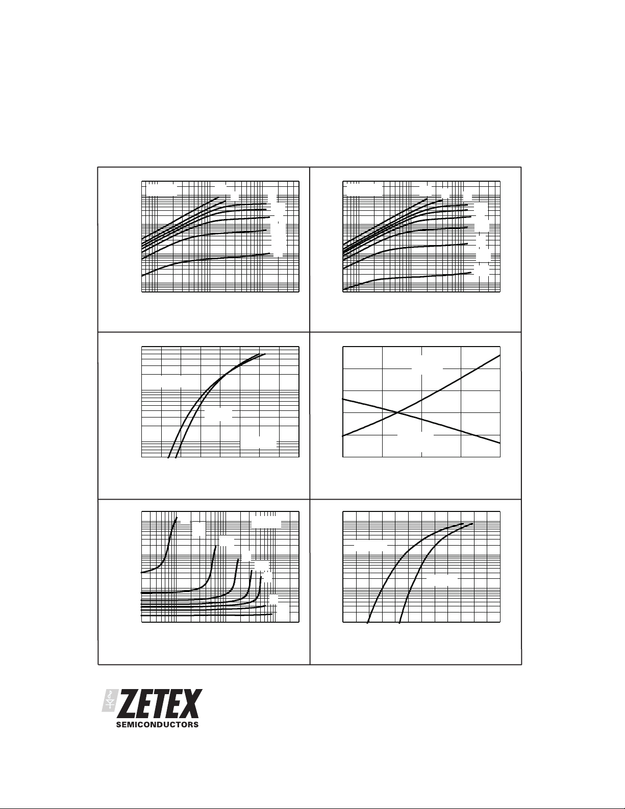
N-CHANNEL TYPICAL CHARACTERISTICS
T = 25°C
10
10V
5V
7V
1
V
GS
D rainC urre n t (A )
0.1
D
I
0.1 1 10
VDSDrain-Source Voltage (V)
Ou tpu t Cha racte ristics
10
VDS= 10V
T = 150°C
1
D rainC urre n t (A )
D
I
0.1
2.0 2.5 3.0 3.5 4.0 4.5 5.0
T=25°C
VGSG a te -S o urceV o lta g e(V )
Typical Transfer Characteristics
4.5V
4V
3.5V
3V
2.5V
10
T = 150°C
7V10V
5V
1
V
D rainC urre n t (A )
0.1
D
I
GS
0.1 1 10
VDSDrain-Source Voltage (V)
Output Characteristics
1.6
1.4
GS(th)
1.2
andV
1.0
DS(on)
0.8
0.6
N or m a lise dR
0.4
-50 0 50 100 150
Tj Junction Temperature (°C)
VGS= 10V
I
=2.5A
D
VGS=V
ID= 250uA
DS
No rm alisedCurv es v Tem p eratu re
4.5V
4V
3.5V
3V
2.5V
2V
R
DS(on)
V
GS(th)
2.5V
3V
1
0.1
Drain-Source On-Resistance
R
T=25°C
DS(on)
0.1 1 10
IDD rainCu rre n t (A )
O n-R e s is t anc evD r ainCu r r e nt
3.5V
4V
4.5V
V
5V
10V
GS
7V
10
T = 150°C
1
T = 25°C
0.1
Reverse Drain Current (A)
SD
I
0.4 0.6 0.8 1.0 1.2
VSDSource-Drain Voltage (V)
Source-Drain Diode Forward Voltage
PROVISIONAL ISSUE E - JULY 2004
6

N-CHANNEL TYPICAL CHARACTERISTICS
ZXMC3AM832
300
250
200
150
100
50
C Capacitance (pF)
0
0.1 1 10
C
ISS
VDS-Drain-SourceVoltage(V)
C
OSS
VGS=0V
f=1MHz
C
RSS
10
ID=2.5A
8
6
4
2
G ate-S o urc eVo ltag e(V)
GS
0
V
01234
VDS= 15V
Q - Charge (nC)
Gate-Source Voltage v Gate ChargeCapacitance v Drain-Source Voltage
PROVISIONAL ISSUE E - JULY 2004
7
ZXMC3AM832
P-CHANNEL TYPICAL CHARACTERISTICS
10V
5V
4V
3.5V
3V
2.5V
-V
2V
GS
0.1
10
T=25°C
1
Drain Current (A)
D
0.01
-I
0.1 1 10
-VDSDrain-Source Voltage (V)
Ou tpu t Cha racte ristics
T = 150°C
1
T=25°C
Drain Current (A)
0.1
D
-I
-VDS=10V
12345
-VGSGate-Source Voltage (V)
Typical Transfer Characteristics
10
T = 150°C
10V
5V
4V
1
0.1
Drain Current (A)
D
0.01
-I
0.1 1 10
-VDSDrain-Source Voltage (V)
Ou tpu t Cha racte ristics
1.6
1.4
GS (th )
andV
1.2
DS(on)
1.0
0.8
N o rmalisedR
0.6
-50 0 50 100 150
VGS=-10V
=-1.4A
I
D
VGS=V
DS
ID= -250uA
V
Tj Junction Temperature (°C)
No rm alisedCurv es v Tem p eratu re
R
GS(th )
3.5V
3V
2.5V
2V
-V
1.5V
DS(on)
GS
100
2V
-V
GS
2.5V
10
1
Drain-SourceOn-Resistance (Ω)
0.1
DS(on)
R
0.1 1 10
-IDDrain Current (A)
On -Re sistancev Drain Curren t
3V
T=25°C
3.5V
4V
5V
10V
10
T = 150°C
1
0.1
T=25°C
Reverse DrainCurrent(A)
SD
-I
0.01
0.2 0.4 0.6 0.8 1.0 1.2 1.4
-VSDSource-Drain Voltage (V)
Source-Drain Diode Forward Voltage
PROVISIONAL ISSUE E - JULY 2004
8

P-CHANNEL TYPICAL CHARACTERISTICS
ZXMC3AM832
300
250
200
150
100
50
C Capacitance (pF)
0
0.1 1 10
C
ISS
C
VGS=0V
f=1MHz
OSS
C
RSS
-VDS-Drain-SourceVoltage(V)
Capacitance v Drain-Source Voltage
10
ID= -1.4A
8
6
4
2
G ate -S o u rceVo ltag e(V )
0
GS
0246
-V
Q- Charge(nC)
VDS= -15V
Gate-SourceVoltagevGateCharge
PROVISIONAL ISSUE E - JULY 2004
9

ZXMC3AM832
MLP832 PACKAGE OUTLINE (3mm x 2mm Micro Leaded Package)
CONTROLLING DIMENSIONS IN MILLIMETERS APPROX. CONVERTED DIMENSIONS IN INCHES
PACKAGE DIMENSIONS
DIM
Millimeters Inches
Min Max Min Max Min Max Min Max
DIM
Millimeters Inches
A 0.80 1.00 0.0315 0.0394 e 0.65 BSC 0.0256 BSC
A1 0.00 0.05 0.00 0.002 E 2.00 BSC 0.0787 BSC
A2 0.65 0.75 0.0256 0.0295 E2 0.43 0.63 0.017 0.0248
A3 0.15 0.25 0.006 0.0098 L 0.20 0.45 0.0079 0.0177
b 0.24 0.34 0.0095 0.0134 L2 0.00 0.125 0.00 0.005
b1 0.17 0.30 0.0068 0.0118 r 0.075 BSC 0.0029 BSC
D 3.00 BSC 0.118 BSC ⍜ 0⬚ 12⬚ 0⬚ 12⬚
D2 0.82 1.02 0.0323 0.0402 - ---D3 1.01 1.21 0.0398 0.0476 - ----
© Zetex Semiconductors plc 2004
Europe
Zetex GmbH
Streitfeldstraße 19
D-81673 München
Germany
Telefon: (49) 89 45 49 49 0
Fax: (49) 89 45 49 49 49
europe.sales@zetex.com
These offices are supported by agents and distributors in major countries world-wide.
Thispublication isissuedto provideoutlineinformation onlywhich(unless agreedbythe Companyinwriting) maynotbe used,appliedor reproduced
for any purpose orform partof any order or contractor beregarded as a representation relatingto theproducts or services concerned. TheCompany
reserves the right to alter without notice the specification, design, price or conditions of supply of any product or service.
For the latest product information, log on to www.zetex.com
Americas
Zetex Inc
700 Veterans Memorial Hwy
Hauppauge, NY 11788
USA
Telephone: (1) 631 360 2222
Fax: (1) 631 360 8222
usa.sales@zetex.com
Asia Pacific
Zetex (Asia) Ltd
3701-04 Metroplaza Tower 1
Hing Fong Road, Kwai Fong
Hong Kong
Telephone: (852) 26100 611
Fax: (852) 24250 494
asia.sales@zetex.com
Corporate Headquarters
Zetex Semiconductors plc
Lansdowne Road, Chadderton
Oldham, OL9 9TY
United Kingdom
Telephone (44) 161 622 4444
Fax: (44) 161 622 4446
hq@zetex.com
10
PROVISIONAL ISSUE E - JULY 2004
 Loading...