

Zetex ZXM62N03E6TA, ZXM62N03E6TC Datasheet
30V N-CHANNEL ENHANCEMENT MODE MOSFET
SUMMARY
V
(BR)DSS
DESCRIPTION
This new generation of high density MOSFETs from Zetex utilise a unique
structure that combines the benefits of low on-resistance with fast switching
speed. This makes them ideal for high efficiency, low voltage, power
management applications.
FEATURES
• Low on-resistance
• Fast switching speed
• Low threshold
• Low gate drive
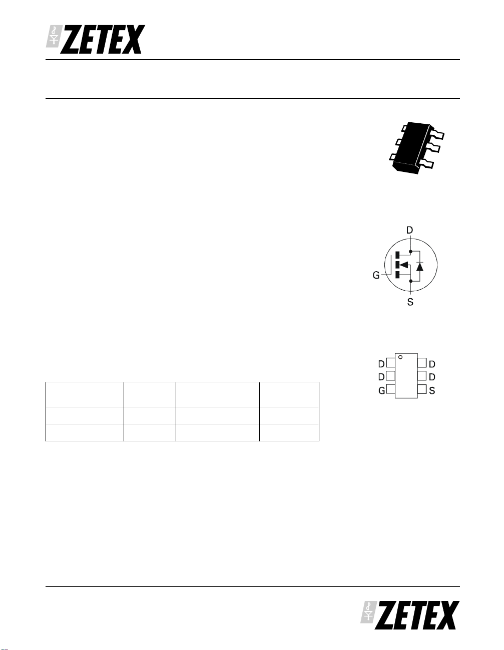
• SOT23-6 package
APPLICATIONS
• DC - DC Converters
• Power Management Functions
• Disconnect switches
• Motor control
ORDERING INFORMATION
DEVICE REEL SIZE
ZXM62N03E6TA 7 8mm embossed 3000 units
ZXM62N03E6TC 13 8mm embossed 10000 units
=30V; R
DS(ON)
(inches)
=0.11V; ID=3.2A
TAPE WIDTH (mm) QUANTITY
PER REEL
ZXM62N03E6
SOT23-6
Top View
DEVICE MARKING
• 2N03
PROVISIONAL ISSUE A - MAY 1999
97

ZXM62N03E6
ABSOLUTE MAXIMUM RATINGS.
PARAMETER SYMBOL LIMIT UNIT
Drain-Source Voltage V
Gate Source Voltage V
Continuous Drain Current (V
(V
=10V; TA=25°C)(b)
GS
=10V; TA=70°C)(b)
GS
Pulsed Drain Current (c) I
Continuous Source Current (Body Diode) (b) I
Pulsed Source Current (Body Diode) I
Power Dissipation at T
Linear Derating Factor
Power Dissipation at T
Linear Derating Factor
=25°C (a)
A
=25°C (b)
A
DSS
GS
I
D
DM
S
SM
P
D
P
D
THERMAL RESISTANCE
PARAMETER SYMBOL VALUE UNIT
Junction to Ambient (a) R
Junction to Ambient (b) R
NOTES
(a) For a device surface mounted on 25mm x 25mm FR4 PCB with high coverage of single sided 1oz copper,
in still air conditions
(b) For a device surface mounted on FR4 PCB measured at t<5 secs.
(c) Repetitive rating - pulse width limited by maximum junction temperature. Refer to Transient Thermal
Impedance graph.
θJA
θJA
30 V
± 20
3.2
V
A
2.6
18 A
2.1 A
18 A
1.1
8.8
1.7
13.6
W
mW/°C
W
mW/°C
113 °C/W
73 °C/W
PROVISIONAL ISSUE A - MAY 1999
98
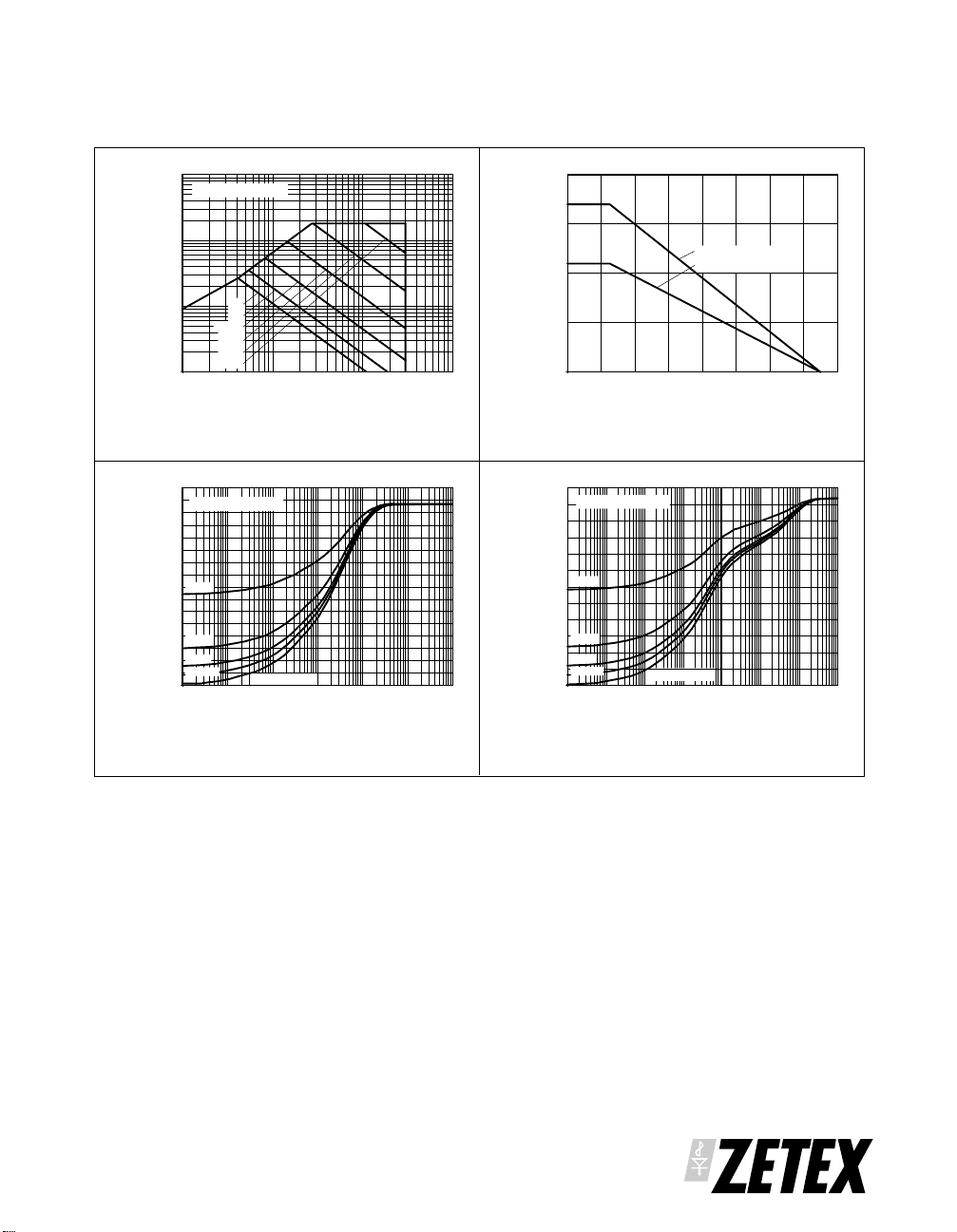
CHARACTERISTICS
ZXM62N03E6
100
Refer Note (a)
10
1
- Drain Current (A)
D
I
0.1
DC
1s
100ms
10ms
1ms
100µs
0.1 10 100
1
VDS- Drain-Source Voltage (V)
Safe Operating Area
80
60
40
20
Thermal Resistance (°C/W)
0
0.0001 0.1 100
D=0.5
D=0.2
D=0.1
D=0.05
Refer Note (b)
Single Pulse
0.01 100.001 1
Pulse Width (s)
Transient Thermal Impedance
2
1.5
Refer No te (b)
1
Refer Note (a)
0.5
0
Max Power Dissipation (Watts)
080160
60 14020 40 100 120
T - Temperature (°)
Derating Curve
120
100
80
60
40
20
Thermal Resistance (°C/W)
0
0.0001 10000.001 0.01 0.1 1 10
D=0.5
D=0.2
D=0.1
D=0.05
Refer Note (a)
Pulse Width (s)
Single Pulse
100
Transient Thermal Impedance
PROVISIONAL ISSUE A - MAY 1999
99
 Loading...