ZXLD1601
ADJUSTABLE DC - DC BOOST CONVERTER WITH INTERNAL SWITCH
IN SC70
DESCRIPTION
The ZXLD1601 is a PFM inductive boost converter
designed to provide output voltages of up to 28V from
a 2.5V to 5.5V input supply.
The ZXLD1601 includes the output switch and peak
current sense resistor, and can provide up to 10mA
output current at maximum output voltage. Higher
current is available at lower output voltages.
Quiescent current is typically 60A and a shutdown
function is provided to reduce this current to less than
100nA in the ‘off’ state.
ADVANCED FEATURES
Internal 30V NDMOS switch, current sense and
•
output setting resistors.
Output voltage is set to a nominal value between 26V
and 28V, by an internal resistor network, but can be
adjusted to lower values by external resistors, an
external PWM control signal applied to the ‘Enable’
pin, or a combination of the two. Depending upon the
control frequency, the PWM signal will provide either
continuous (low ripple) or gated control. The PWM
filter components are contained within the chip.
Minimum output voltage is determined by the input
supply.
The device is assembled in a low profile SC70-6 pin
package.
APPLICATIONS
LCD and OLED bias
•
True analogue output voltage control via PWM
•
with internal filter
FEATURES
Low profile SC70-6 pin package
•
•
Internal PWM filter for adjustable output
•
High efficiency (85% typ)
•
Wide input voltage range: 2.5V to 5.5V
•
Up to 250mA output current at 5V
•
Low quiescent current: (60A typ)
•
100nA maximum shutdown current
•
Up to 1MHz switching frequency
•
Low external component count
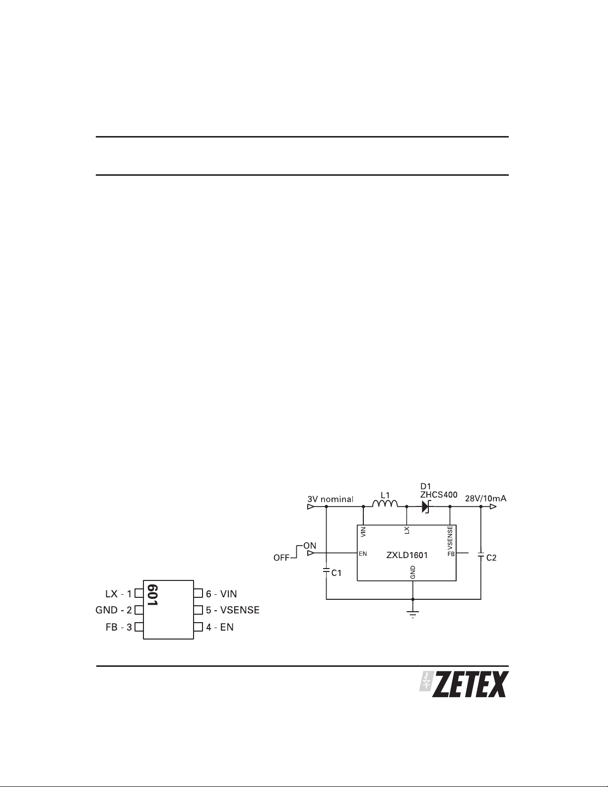
PINOUT
Cellular / mobile phones
•
Digital cameras
•
PDAs
•
•
LCD modules
•
Varactor and PIN diode bias
•
Palmtop computers
TYPICAL APPLICATION CIRCUIT
TOP VIEW
ISSUE 3 - AUGUST 2004
1
SEMICONDUCTORS

ZXLD1601
ABSOLUTE MAXIMUM RATINGS
(Voltages to GND unless otherwise stated)
Input voltage (V
LX output voltage (V
Switch output current (I
Power dissipation (PD) 300mW
Operating temperature (T
Storage temperature (T
Junction temperature (Tj
ELECTRICAL CHARACTERISTICS: (Testconditions:V
Symbol Parameter Conditions Min Typ Max Units
V
IN
I
IN
V
FB
R
1
R
2
f
LX
T
OFF
(2)
T
ON
I
LXpk
R
LX
I
LX(leak)
V
OUT
V
ENH
V
ENL
I
ENL
I
ENH
(3)
T
EN(hold)
)7V
IN
) 30V
LX
) 500mA
LX
) -40 to 85°C
OP
) -55 to 150°C
ST
) 125°C
MAX
IN=VEN
=3V, T
=25°C unless otherwise stated
AMB
(1)
)
Input voltage 2.5 5.5 V
Supply current
60
<10
100
100µAnA
Quiescent
Shutdown
V
EN=VIN,ILX
=0V
V
EN
= 0, Output not switching
FB pin control voltage 0.98 1.07 V
Internal resistor from FB pin
135 k⍀
to GND pin
Internal resistor from FB pin
to V
SENSE
pin
Operating frequency L=10H, V
=28V, 5mA load 600 kHz
OUT
3.45 M⍀
LX output ‘OFF’ time 350 500 ns
LX output ‘ON’ time 5µs
Switch peak current limit L=10H, V
=28V, 5mA load 320 mA
OUT
Switch ‘On’ resistance 1.75 ⍀
Switch leakage current VLX=20V 1 µA
Controller default output
FB pin floating 26 28 V
voltage
EN pin high level Input voltage Device active 1.5 V
IN
EN pin low level Input voltage Device in shutdown 0.4 V
EN pin low level input current VEN=0V -100 nA
EN pin high level input current VEN=VIN 1 A
EN pin turn off delay VENswitched from high to low 120 µs
V
NOTES:
1 Production testing of the device is performed at 25°C. Functional operation of the device over a –40°C to +85°C temperature range is
guaranteed by design, characterization and process control.
2 Nominal ‘on’ time (TONnom) is defined by the input voltage (V
T
= {I
ONnom
3 This is the time for which the device remains active after the EN pin has been asserted low. This delay is necessary to allow the output to be
maintained during dc PWM mode operation.
LX(pkdc)
x L/VIN} +200ns
), coil inductance (L) and peak current (I
IN
) according to the expression:
LXpkdc
ISSUE 3 - AUGUST 2004
SEMICONDUCTORS
2

ZXLD1601
ELECTRICAL CHARACTERISTICS (Cont.): (Test conditions: V
Symbol Parameter Conditions Min Typ Max Units
⌬T/T PWM duty cycle range at
fLPF Internal PWM low pass filter
ALPF Filter attenuation f=30kHz 52.5 dB
⌬T/T
NOTES:
4 The maximum PWM signal frequency during this mode of operation should be kept as low as possible to minimize errors due to the turn-off
‘EN’ input for dc output
voltage control
cut-off frequency
(4)
PWM duty cycle range at
‘EN’ input for ‘gated’ output
voltage control
delay
10kHz<f<100kHz, VENH =VIN 20 100 %
f < 1kHz, VENH =VIN 0 100 %
IN=VEN
=3V, T
=25°C unlessotherwise stated
AMB
4 kHz
(1)
)
ISSUE 3 - AUGUST 2004
3
SEMICONDUCTORS

ZXLD1601
PIN DESCRIPTION
Pin No. Name Description
LX Output of NDMOS switch
1
GND Ground (0V)
2
FB Feedback pin for voltage control loop
3
Nominal voltage 1.025V
EN Enable input (active high to turn on device)
4
Also used to adjust output current by PWM signal.
Connect to V
V
5
SENSE
V
6
IN
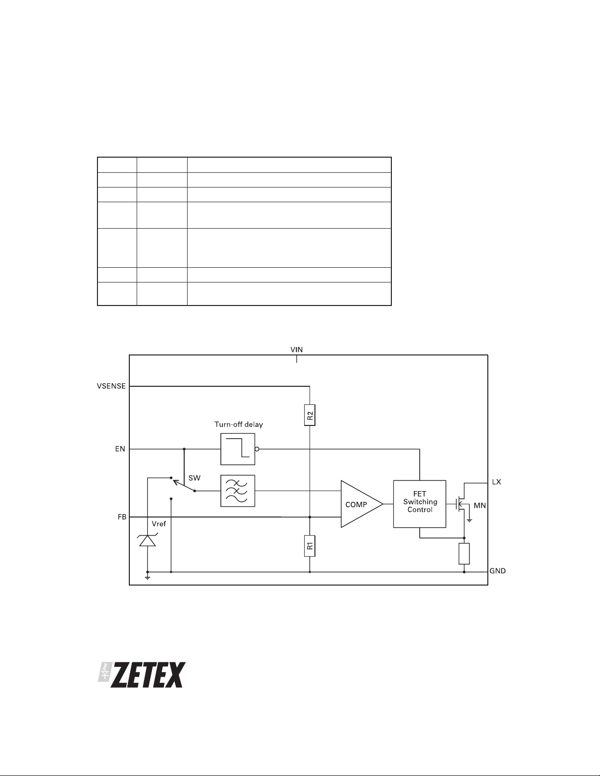
BLOCK DIAGRAM
Output voltage sense
Input voltage (2.5V to 5.5V). Decouple with
capacitor close to device.
for permanent operation.
in
SEMICONDUCTORS
ISSUE 3 - AUGUST 2004
4
 Loading...