

Zetex ZXLD1350EV4 User Manual
ZXLD1350EV4
ZXLD1350EV4 EVALUATION BOARD USER GUIDE
DESCRIPTION
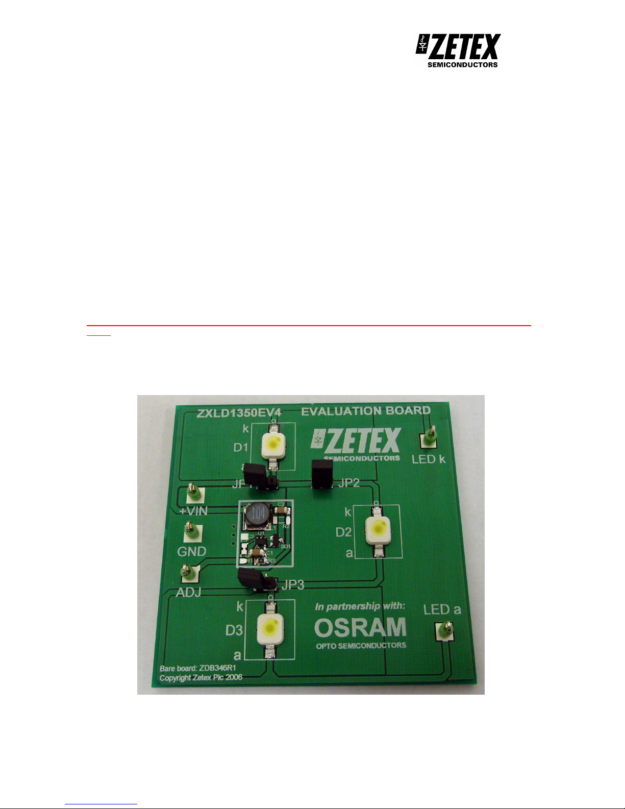
The ZXLD1350EV4, Figure 1, is an evaluation board for evaluating the ZXLD1350 350mA LED driver with internal
switch. The evaluation board can be used to drive 1, 2 or 3 one-watt LEDs, or an external choice of LEDs. The
number of external connected LEDs depends on the forward voltage of the LEDs connected. The LEDs fitted on this
evaluation board are from the Osram range.
The operating voltage is nominally 24V. For three 1W series-connected LEDs, the voltage can be from 12V minimum
to 30V maximum. The 100uH inductor used in the circuit is based on a nominal 24V supply, which should be
connected across +VIN and GND pins. Note: The evaluation board does not have reverse battery protection. The
nominal current for the evaluation board is set at 300mA with a 0.33Ω sense resistor, Rs.
Jumpers J1, J2 and J3 allow the selection of the number of LEDs to be connected in series. Jumper on at J1
bypasses LED D1. Jumper on at J3 bypasses LED D3. Removing jumper J2 disconnects all the on-board LEDs from
the current flow path. Jumper 2 also doubles as a connection point for an ammeter to measure the LED current.
Before connecting external LEDs across test pins LED+ and LED-, or across J1, remove jumper J2. Jumpers J1 and
J2 can be on or off.
Test point ADJ provides a connection point for DC or PWM dimming and shutdown.
Warning: At 24V nominal operation with 300mA output, the LEDs and the PCB may be hot and the LEDs will be very
bright.
ZXLD1350EV4 User Guide Iss. 1 1/8 10-04-07
Figure 1: ZXLD1350EV4 evaluation board
ZXLD1350EV4
ZXLD1350 DEVICE DESCRIPTION
The ZXLD1350 is a continuous mode inductive driver in a TSOT23-5 package, for driving one or more series
connected LEDs efficiently from a voltage source higher than the LED voltage. The device includes the output
switch and a current sense circuit, which requires an external sense resistor to set the nominal current up to
350mA.
ZXLD1350 DEVICE FEATURES
• Drives one or more series-connected 1W white
LEDs up to 350mA.
• Internal 30V switch.
• Wide input voltage: 7V to 30V.
• Inherent open circuit LED protection.
• Brightness control using DC or PWM.
• Internal PWM filter.
DEVICE APPLICATIONS
• LED flashlights.
• High Power LED driving.
• Low-voltage halogen replacement LEDs.
• Automotive lighting.
• Illuminated signs.
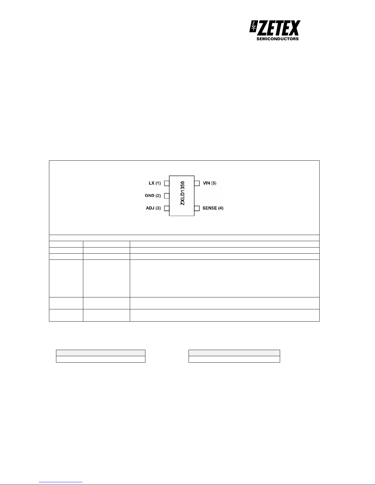
ZXLD1350 Device Packages, Pin and Definitions
TSOT23-5 pack
ZXLD1350 Device Pin Definition
Name Pin No Description
LX 1 Drain of NDMOS switch.
GND 2 Ground (0V).
ADJ 3 Internal voltage ref. pin (1.25V) :
• Leave floating for normal operation.
• Connect to GND to turn off output current.
• Drive with DC voltage (0.3V to 1.25V) or with PWM signal to adjust
output current or....
• Connect a capacitor from this pin to ground to set soft-start time.
ISENSE 4 Connect a sense resistor, Rs, from the ADJ pin to VIN to sense the nominal
VIN 5 Input voltage: 7V to 30V. Decouple to ground with a 1uF or higher ceramic
output current. Nominal I
capacitor.
= 0.1/ Rs
out
ORDERING INFORMATION
EVALBOARD ORDER NUMBER
ZXLD1350EV4
Please note: Evaluation boards are subject to
availability and qualified leads.
ZXLD1350EV4 User Guide Iss. 1 2/8 10-04-07
DEVICE ORDER NUMBER
ZXLD1350E5TA
ZXLD1350EV4
ZXLD1350EV4 EVALUATION BOARD
REFERENCE DESIGN
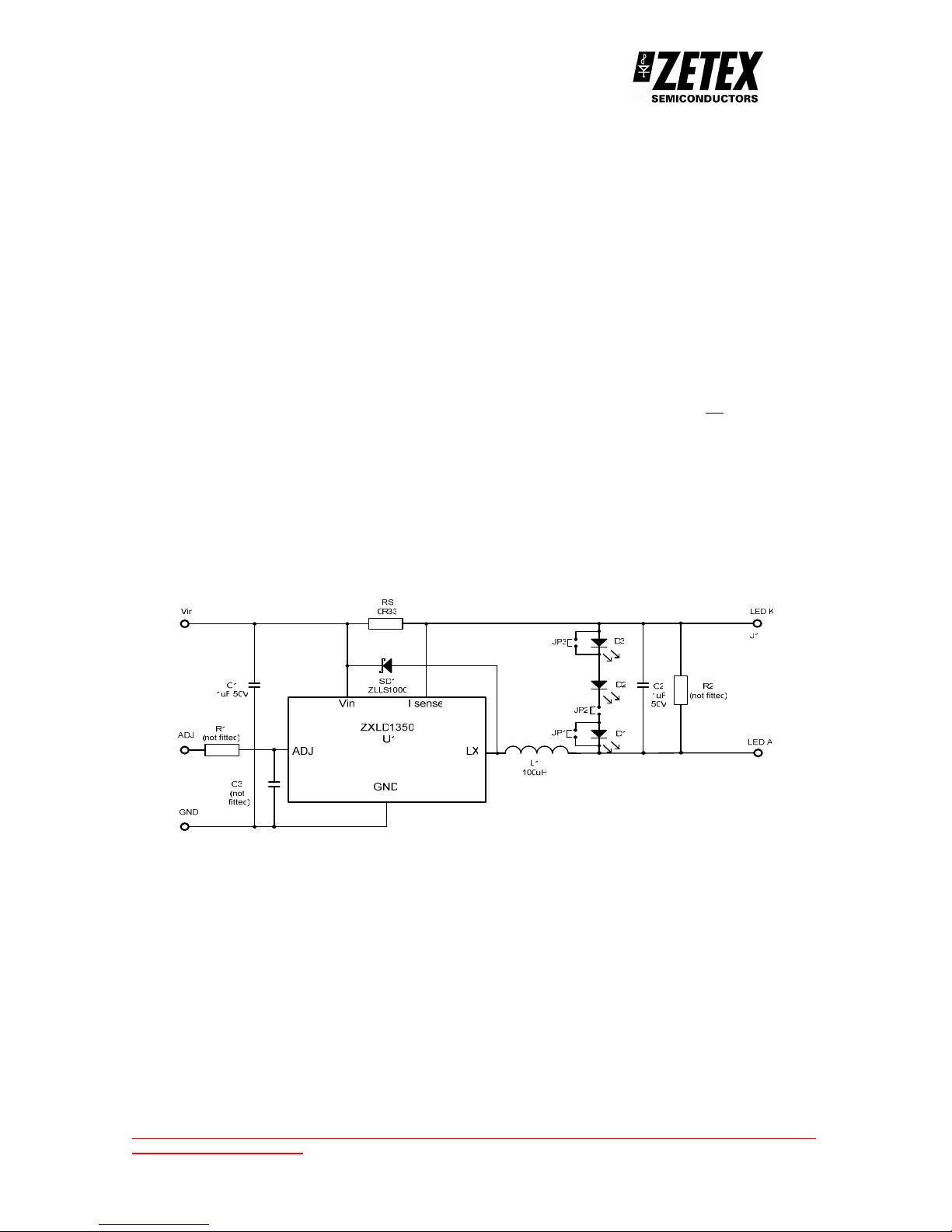
The ZXLD1350EV4 is configured to the reference design in Figure 2. The target application is a driver for one or
more series-connected 1W white LEDs for torches and other high powered LED driving applications.
The operating voltage is a nominal 24V. For three 1W series-connected LEDs, the voltage can be from 12V
minimum to 30V maximum. The nominal current is set at 300mA with a 0.33Ω sense resistor, Rs. For three series
connected 1–watt LEDs, with a nominal supply of 24V, the ZXLD1350 runs in continuous mode at 545kHz, with a
100uH inductor.
Jumpers J1, J2 and J3 allow selection of the number of LEDs to be connected in series. Jumper on at J1 bypasses
LED D1. Jumper on at J3 bypasses LED D3. Removing jumper J2 disconnects all the 1-watt LEDs from the current
flow path. Jumper 2 also doubles as a connection point for an ammeter to measure the LED current.
Both DC and PWM dimming can be achieved by driving the ADJ pin. For DC dimming, the ADJ pin may be driven
between 0.3V and 1.25V. Driving the ADJ pin below 0.2V will shutdown the output current. For PWM dimming, an
external open-collector NPN transistor or open-drain N-channel MOSFET can be used to drive the ADJ pin. The
PWM frequency can be low, around 100Hz to 1kHz, or high between 10kHz to 50kHz. C3 should not be fitted on the
evaluation board when using the PWM dimming feature. Shorting R1 will connect the test pin ADJ to device pin ADJ.
The capacitor C3 should be around 10nF to decouple high frequency noise at the ADJ pin for DC dimming.
The soft-start time will be nominally 0.5ms without capacitor C3. Adding C3 will increase the soft start time by
approximately 0.5ms/nF
For other reference designs or further applications information, please refer to the ZXLD1350 datasheet.
Schematic Diagram
Figure 2 shows the schematic for the ZXLD1350EV4 evaluation board.
-
Figure 2: Schematic for the evaluation board ZXLD1350EV4
ZXLD1350 Operation
In normal operation, when voltage is applied at +VIN, the ZXLD13350 internal NDMOS switch is turned on. Current
starts to flow through sense resistor Rs, inductor L1, and the LEDs. The current ramps up linearly, and the ramp rate
is determined by the input voltage +VIN and the inductor L1. This rising current produces a voltage ramp across Rs.
The internal circuit of the ZXLD1350 senses the voltage across Rs and applies a proportional voltage to the input of
the internal comparator. When this voltage reaches an internally set upper threshold, the NDMOS switch is turned off.
The inductor current continues to flow through Rs, L1, the LEDs, the schottky diode SD1, and back to the supply rail,
but it decays, with the rate of decay determined by the forward voltage drop of the LEDs and the schottky diode. This
decaying current produces a falling voltage at Rs, which is sensed by the ZXLD1350. A voltage proportional to the
sense voltage across Rs is applied at the input of the internal comparator. When this voltage falls to the internally set
lower threshold, the NDMOS switch is turned on again. This switch-on-and-off cycle continues to provide the average
LED current set by the sense resistor Rs. Please refer to the datasheets for the threshold limits, ZXLD1350 internal
circuits, electrical characteristics and parameters.
Warning: At a nominal 24V operation with 300mA output, the board temperature rises by around 30C from ambient
after 30 minutes of operation.
ZXLD1350EV4 User Guide Iss. 1 3/8 10-04-07
 Loading...