Zetex ZXLB1600X10TA, ZXLB1600X10TC Datasheet

ZXLB1600
LCD BIAS BOOST CONVERTER
DESCRIPTION
The ZXLB1600 DC/DC boost converter accepts an input voltage of between 1.6V and 5.5V and
provides an adjustable output voltage of up to 28V for LCD backplane bias. The device contains the
output switch and a second switch to isolate the coil from the input and provide true isolation in
shutdown mode. The output can be adjusted by means of an externally applied dc voltage, or PWM
control signal and can supply typically 10mA of output current at maximum output voltage. Higher
current is available at lower output voltages.
The input voltage range accepts a number of battery solutions, including dual dry cell and single Li-Ion
cells and PFM operation mode allows the output to be regulated with high efficiency under light or no
load conditions. The switching frequency range permits the use of miniature surface mount inductors.
The voltage control range can be modified, if required, by external resistors. A low battery comparator
is provided to indicate when the input voltage has fallen to within ±2% of a preset threshold.
FEATURES
• Wide input voltage range: 1.6 to 5.5V
• Adjustable output voltage up to 28V using PWM or analog control voltage
• True shutdown (output isolated from input)
• Internal output switch and current sense
• Low quiescent current: (75
µA (max) shutdown current (including low battery comparator)
• 5
• Up to 500kHz switching frequency (PFM)
• 85% efficiency
• Low battery flag
• Small MSOP10 package
• Low external component count
µA max)
APPLICATIONS
• PDAs
• Mobile Phones
• Digital Cameras
• Portable Internet Appliances
• Notebook and Palmtop computers
ORDERING INFORMATION
DEVICE DEVICE DESCRIPTION TEMPERATURE RANGE PART MARK TAPING
OPTIONS
ZXLB1600X10 Boost converter for LCD
bias in MSOP10
TA reels 500 devices, TC reels 2500 devices
DRAFT ISSUE J January 2002
0 °C to 70 °C
ZXLB1600 TA, TC
ZXLB1600
1

ZXLB1600
ABSOLUTE MAXIMUM RATINGS
(Voltages to GND unless otherwise stated)
Output Voltage
Input Voltage
Switch output current
Power Dissipation
Operating Temperature 0 to 70°C
Storage Temperature -55 to 125°C
Junction Temperature 150°C
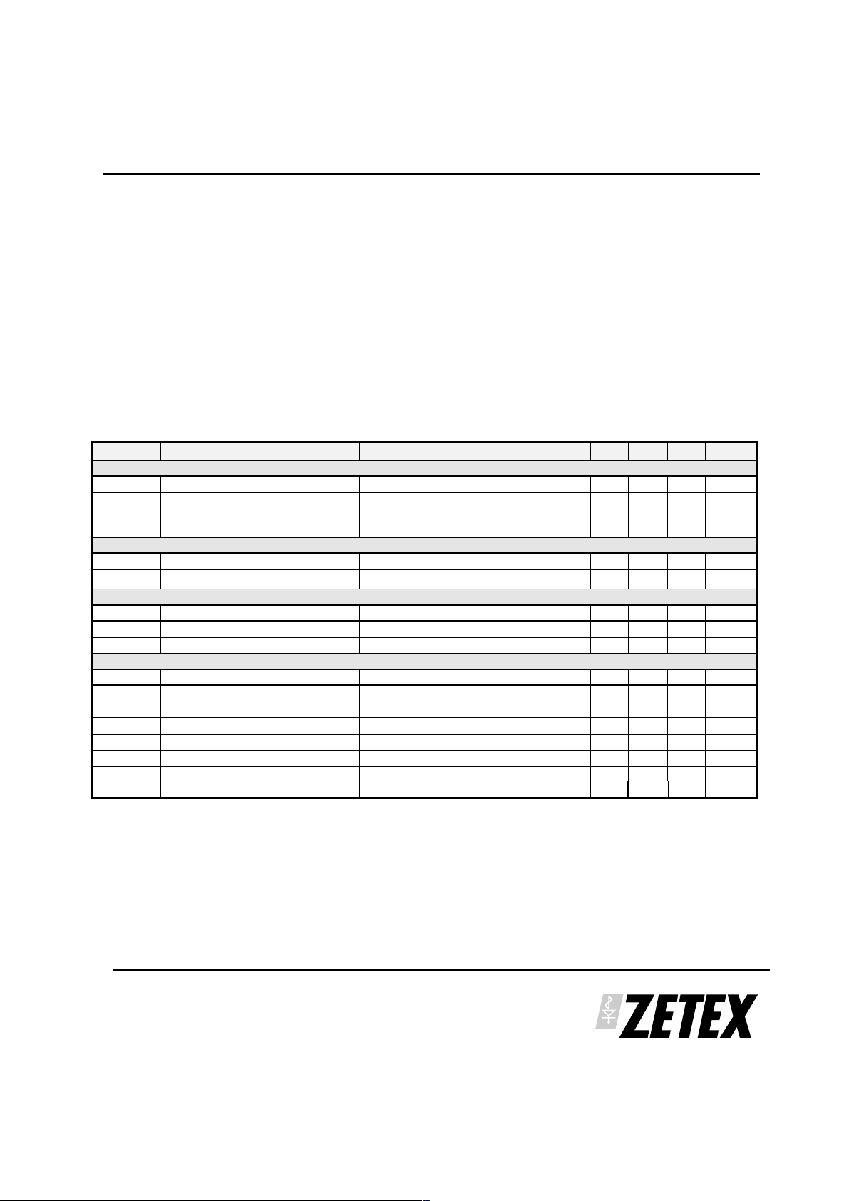
ELECTRICAL CHARACTERISTICS:
Test conditions unless otherwise stated: V
Symbol Parameter Conditions Min Typ Max Units
V
IN
I
IN
R
ISO
I
ISO
I
LX
R
LX
I
LX(leak)
V
OUT
I
OUT
∆V
LNR
∆V
LDR
f
LX
T
ON
T
OFF
ξ
Input voltage 1.6 3 5.5 V
Supply current
Shutdown
Quiescent
‘On’ resistance VEN = V
Leakage current V
Switch peak current limit 0.2 0.3 0.5 A
‘On’ resistance 1.0 2
Switch leakage current 1 µA
Output voltage range V
Maximum output current Lx = 22µH, V
Line regulation I
Load regulation V
Operating frequency 200 500 kHz
Output ‘ON’ time LX output low 10 µs
Output ‘OFF’ time LX output off 1 µs
Efficiency V
30V
7V
500mA
800mW
=3.0V, T
IN
AMB
=25°°°°C
General
V
V
= 0V, V
EN
= VIN, I
EN
=5.5V (Note 1)
IN
= 0V
OUT
3575µA
Isolating switch
IN
= 0V 1 µA
EN
0.8 2
LX Switch
Controller output
IN
= 28V 5 10 mA
OUT
= 1mA, 2V < VIN <5.5V 0.1 %/V
OUT
= 28V, 100uA < I
OUT
= 28V, I
OUT
= 1mA, L=22µH 85 %
OUT
< 5mA 0.01 %/mA
OUT
µA
Ω
Ω
29 V
Note:1 Shutdown current includes 3µA (max) for the battery low comparator, which remains active in shutdown
mode
DRAFT ISSUE J January 2002
ZXLB1600
2

ZXLB1600
(
)
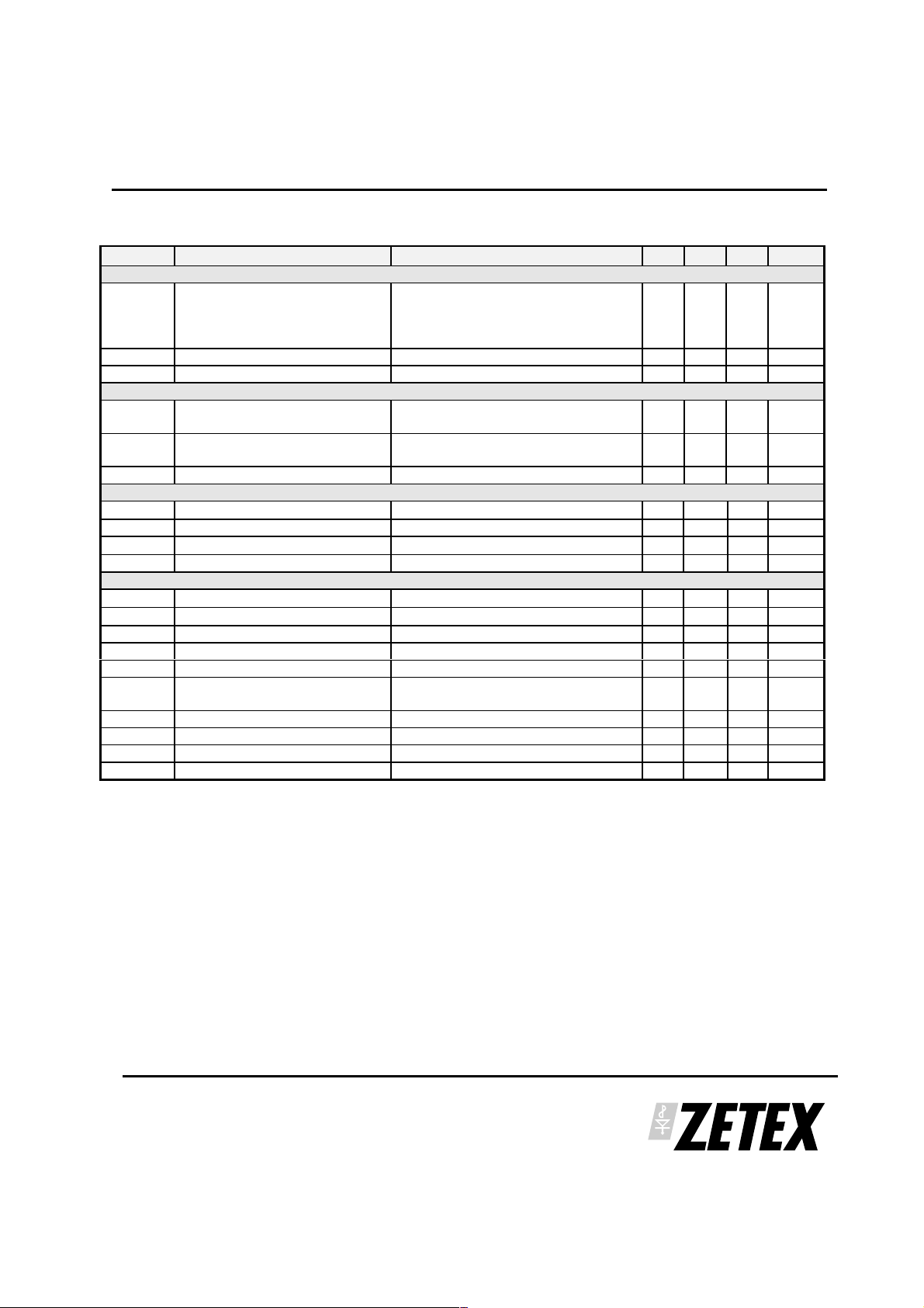
Test conditions unless otherwise stated: VIN=3.0V, T
AMB
=25°°°°C
Symbol Parameter Conditions Min Typ Max Units
Output Voltage control by dc voltage applied to ‘ADJ’ pin
V
ADJ (NOM)
V
ADJ
I
ADJ
V
SENSE
∆T/T
f
LPF
A
LPF
V
ENL
V
ENH
I
ENL
I
ENH
I
BLQ
V
BLT
V
BTOL
V
BLHYS
V
LBT
V
LBT (max)
I
BLOL
V
BLOL
I
BLOH
V
BLOH
Internal reference voltage ‘ADJ’ pin floating, ‘EN’= V
External overdrive voltage range
on ‘ADJ’ pin for output voltage
IN
1.23 V
0.5 V
ADJ
NOM
V
control
Input current 0.5<V
ADJ < VADJ (NOM)
Output voltage ‘ADJ’ pin floating, ‘EN’= V
IN
27 29 V
-10 µA
Output Voltage control by PWM signal applied to ‘EN’ input
PWM duty cycle range at ‘EN’
10kHz < f < 100kHz, V
ENH
=V
IN
40 100 %
input
Internal low pass filter cut-off
4kHz
frequency
Filter attenuation F=30kHz 52.5 dB
Enable input
Low level Input voltage Device in shutdown 0.4 V
High level Input voltage Device active 1.4 Vin V
Low level input current V
High level input current V
=0V -100 nA
EN
=VIN 100 nA
EN
Battery low comparator
Quiescent current VIN =5.5V 3 µA
Detection threshold VIN falling 2 V
Threshold tolerance +/-2 %
Hysteresis V
rising 20 mV
IN
Threshold voltage on LBT pin LBT floating 1.21 V
Maximum voltage on LBT pin
during normal device operation
Vin-
0.5
V
Low level output current Output ‘on’ 1 mA
Low level output voltage I
= 1mA 0.4 V
BLOL
High level output current Output ‘off’ 2 µA
High level output voltage Output ‘off’ 29 V
DRAFT ISSUE J January 2002
ZXLB1600
3
 Loading...