

ZXLB1600
LCD AND OLED BIAS BOOST CONVERTER - STN, CSTN SCREENS
DESCRIPTION
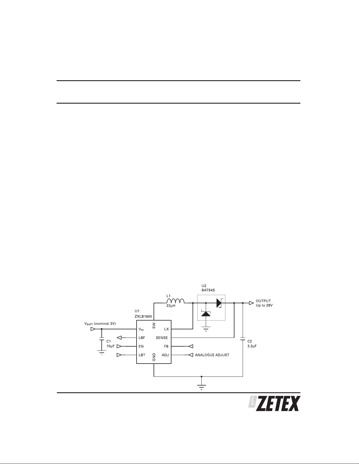
The ZXLB1600 inductive switching boost converter
accepts an input voltage of between 1.6V and 5.5V and
provides an adjustable output voltage of up to 28V for
LCD and OLED bias. The device contains an output
switch and a second switch to isolate the coil from the
input to provide true isolation in shutdown mode. The
output can be adjusted by means of an externally
applied dc voltage, a PWM control signal, or external
feedback resistors and can supply typically 10mA of
output current at maximum output voltage. Higher
current is available at lower output voltages.
The input voltage range accepts a number of battery
solutions, including dualdrycellandsingleLi-Ioncells
and PFM operation mode allows the output to be
regulated with high efficiency under light or no load
conditions.Theswitchingfrequencyrangepermitsthe
use of miniature surface mount inductors.
A low battery comparator is provided to indicate when
the input voltage has fallen to within ±2% of a preset
threshold. This threshold is set internally , but can be
adjusted externally to any voltage within the supply
voltage range.
TYPICAL APPLICATION CIRCUIT
FEATURES
Wide input voltage range: 1.6 to 5.5V
•
Adjustable output voltage up to 28V, using PWM
•
or analog control voltage
Internal PWM filter
•
True shutdown (output isolated from input)
•
Internal output switch and current sense
•
Low quiescent current: (75A max)
•
5A (max) shutdown current (including low
•
battery comparator)
Up to 500kHz switching frequency
•
High efficiency
•
Small MSOP10 package
•
Low external component count
•
APPLICATIONS
PDAs
•
•
Mobile phones - OLED sub displays
•
Digital cameras
•
Portable internet appliances
•
Palmtop computers
•
GPS terminals
ISSUE 3 - SEPTEMBER 2003
1
SEMICONDUCTORS
ZXLB1600
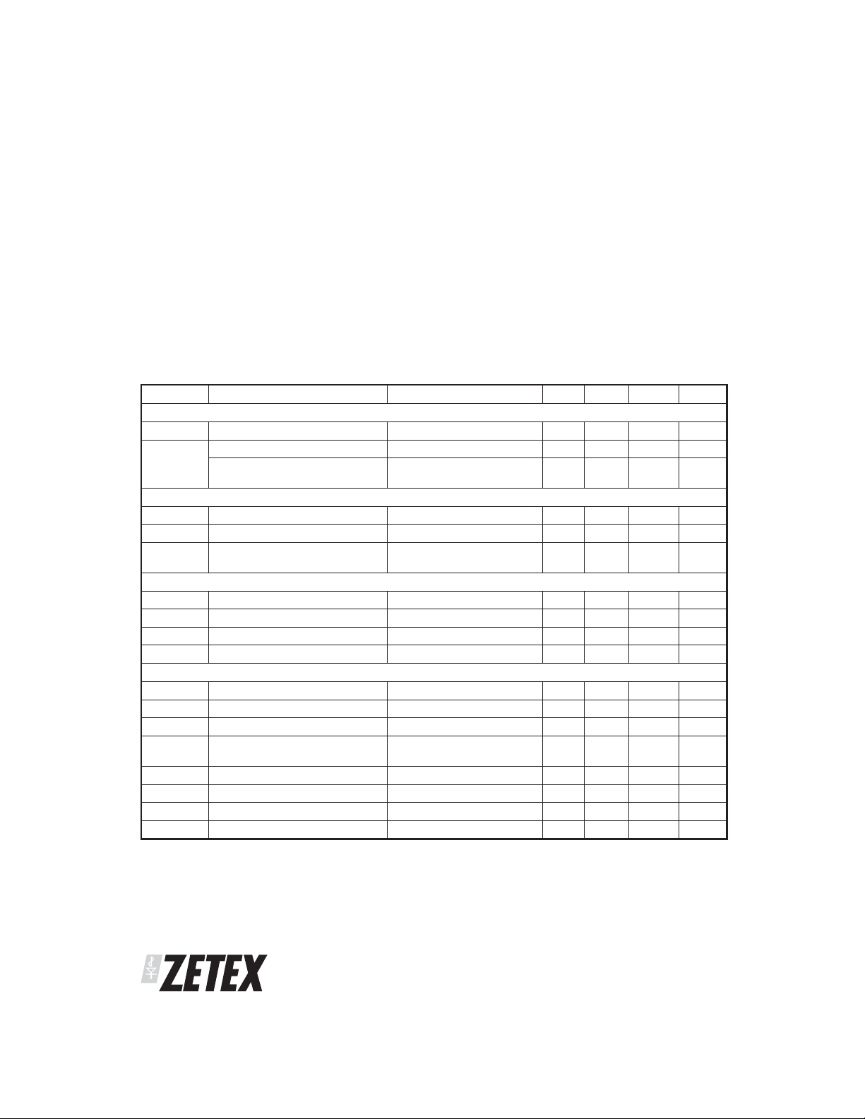
ABSOLUTE MAXIMUM RATINGS
(Voltages to GND unless otherwise stated)
Output voltage 30V
Input voltage 7V
Switch output current 500mA
Power dissipation 800mW
Operating temperature 0 to 70⬚C
Storage temperature -55 to 125⬚C
Junction temperature 150⬚C
ELECTRICAL CHARACTERISTICS
Test conditions unless otherwise stated: V
Symbol Parameter Conditions Min Typ Max Units
General
V
IN
I
IN
Input voltage
Supply current Shutdown
Quiescent VEN=VIN,I
Isolating switch
R
ISO
I
ISO
V
SW(max)
‘On’ resistance VEN=V
Leakage current VEN=0V 1 A
Maximum voltage on SW pin
during normal operation
LX Switch
I
LX
R
LX
I
LX(leak)
V
LX
Switch peak current limit
‘On’ resistance 0.5 2 ⍀
Switch leakage current 1 A
Operating voltage on LX pin -0.5 30 V
Controller output
V
I
OUT
⌬V
⌬V
f
LX
T
T
OUT
LNR
LDR
ON
OFF
Output voltage range V
Output current Lx = 22H, V
Line regulation I
Load regulation V
Operating frequency 500 kHz
Output ‘ON’ time LX output low 10 s
Output ‘OFF’ time LX output off 0.9 µs
Efficiency
Note:
1) Minimum supply voltage should be maintained above 2V for operation at minimum temperature.
2) Shutdown current includes the operating current for the low battery comparator, which remains active in shutdown mode.
3) This is the dc value. The dynamic value may exceed 350mA during normal operation, due to switching delays, coil inductance and supply
voltage.
4) Efficiency is dependent upon the choice of external components, input/output voltages and load current.(see typical operating curves).
(1)
(2)
(3)
(4)
= 3.0V, T
IN
AMB
= 25°C
1.6 5.5 V
VEN= 0V 3.5 5 A
switching
IN
OUT
= 0V, Not
30 75 A
0.7 2 ⍀
VIN+0.5 V
0.15 0.35 A
IN
= 28V 5 10 mA
OUT
= 1mA, 2V < VIN<5.5V 0.1 %/V
OUT
= 28V, 100A<I
OUT
< 5mA
Lx=22H, V
OUT
= 20V 80 %
OUT
0.15 %/mA
28 V
SEMICONDUCTORS
ISSUE 3 - SEPTEMBER 2003
2
ZXLB1600
ELECTRICAL CHARACTERISTICS (Cont.)
Test conditions unless otherwise stated: V
Symbol Parameter Conditions Min Typ Max Units
Output voltage control by dc voltage applied to ‘ADJ’ pin
V
ADJ (nom)
V
ADJ
I
ADJ
V
SENSE
Output voltage control by PWM signal applied to ‘EN’ input
∆T/T
f
LPF
A
LPF
Internal voltage setting resistors for output voltage
R1 Ref. Block diagram 317
R2 6.93 M⍀
Enable input
V
ENL
V
ENH
I
ENL
I
ENH
T
EN(hold)
Low-battery detection circuit
V
LBT
V
BLHYS
Ref
(LBD)
V
LBT (max)
I
BLOL
V
BLOL
I
BLOH
V
BLOH
Internal voltage setting resistors for low-battery detection circuit
R3 Ref. block diagram 1.56 M⍀
R4 2.44
Note:
5) This is the minimum PWM frequency to maintain a continuous output. Lower frequencies can be used, but will result in gated operation of
the device i.e. device enters shutdown when EN is low (see Note 6).
6) This is the time for which the device remains active after the EN pin has been driven low. This delay allows a continuous output to be
maintained during PWM mode operation at frequencies higher than 10kHz.
Internal reference voltage ‘ADJ’ pin floating, ‘EN’= V
Temperature coefficient of V
ADJ
External overdrive voltage range
on ‘ADJ’ pin for output voltage
control
Input current into V
pin 0.5<V
ADJ
Default Output voltage ‘ADJ’ pin floating, ‘EN’= V
PWM duty cycle range at ‘EN’
input
Internal low pass filter cut-off
frequency
Filter attenuation f=30kHz 52.5 dB
Low level Input voltage Device in shutdown 0.4 V
High level Input voltage Device active 1.4 Vin V
Low level input current VEN=0V -100 nA
High level input current VEN=V
Enable active hold time
(6)
Detection threshold VINfalling 1.94 2.02 V
Temperature coefficient of V
BLT
Hysteresis VINrising 20 mV
Internal reference voltage 1.21 V
Maximum voltage on LBT pin Vin-0.5 V
Low level output current Output ‘on’ 1 mA
Low level output voltage I
High level output current Output ‘off’ , V
High level output voltage Output ‘off’ 29 V
= 3.0V, T
IN
AMB
= 25°C
IN
1.23 V
40 ppm/⬚C
ADJ<VADJ (NOM)
(5)
10kHz
< f < 100kHz, V
IN
ENH=VIN
0.5 V
27 29 V
40 100 %
ADJ
(NOM)
-10 A
V
4 kHz
k⍀
IN
100 nA
VENswitched from high to low 120 s
20 ppm/⬚C
= 0.5mA 0.4 V
BLOL
= 29V 2 A
BLOH
M⍀
ISSUE 3 - SEPTEMBER 2003
3
SEMICONDUCTORS
ZXLB1600
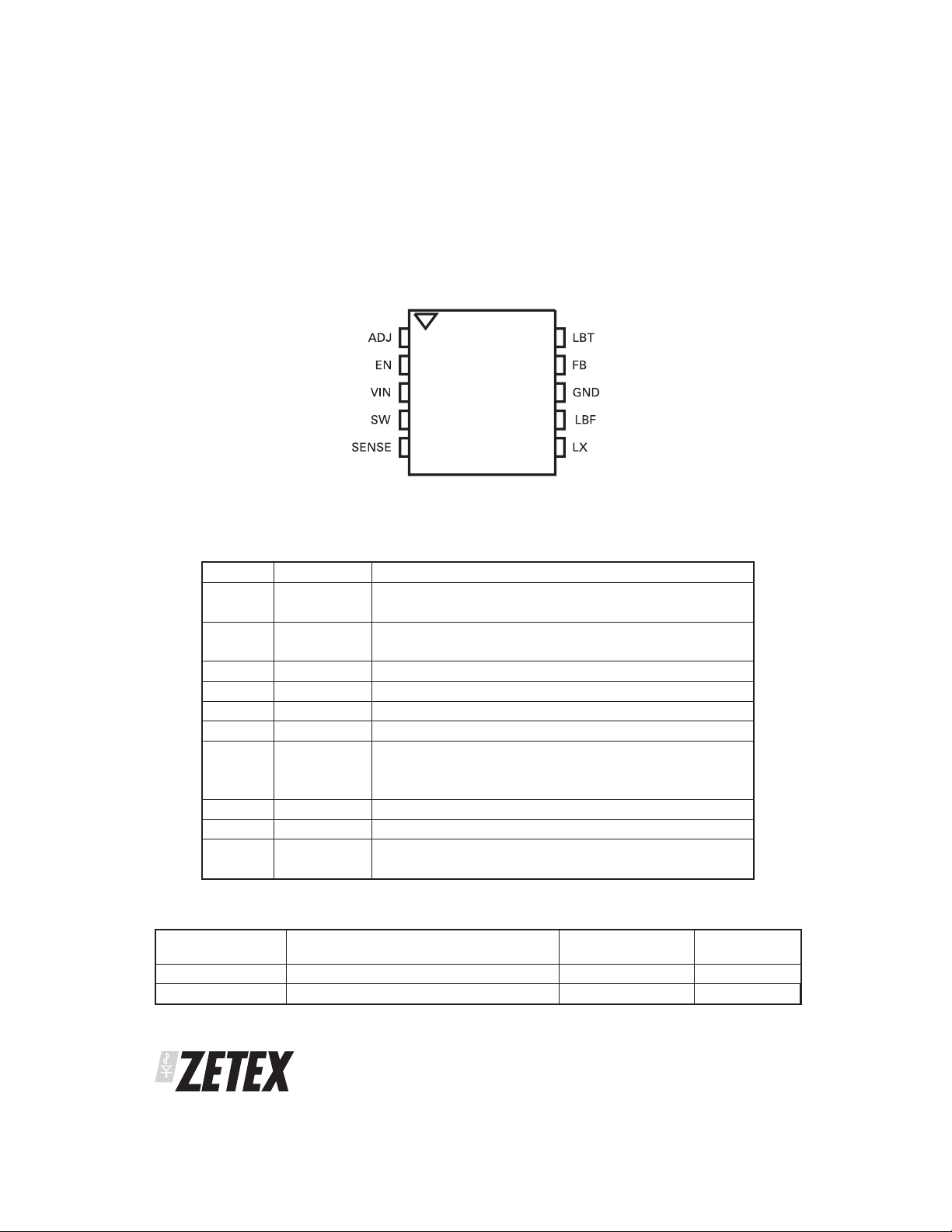
PIN CONNECTIONS
PIN DESCRIPTION
Pin # Name Description
1 ADJ Internal (or external) reference voltage.
2 EN Enable input (active high)
3 VIN Input voltage
4 SW Output of high side PMOS isolation switch
5 SENSE Output voltage sense
6 LX Output of NMOS switch
7 LBF Low battery flag output: open drain
8 GND Ground
9 FB Voltage feedback pin for output (threshold 1.23V)
10 LBT Low battery flag threshold adjust input
Can be overdriven to adjust output voltage
Also used to adjust output voltage by PWM signal
(active low for low battery voltage)
Active when EN is high or low
(threshold 1.21V)
ORDERING INFORMATION
DEVICE DEVICE DESCRIPTION TEMPERATURE
ZXLB1600X10TA Boost converter for LCD bias in MSOP10 0 ⬚C to 70 ⬚C ZXLB1600
ZXLB1600X10TC Boost converter for LCD bias in MSOP10 0 ⬚C to 70 ⬚C ZXLB1600
TA reels 1k,
TC reels 4k devices.
RANGE
ISSUE 3 - SEPTEMBER 2003
SEMICONDUCTORS
4
PART MARK
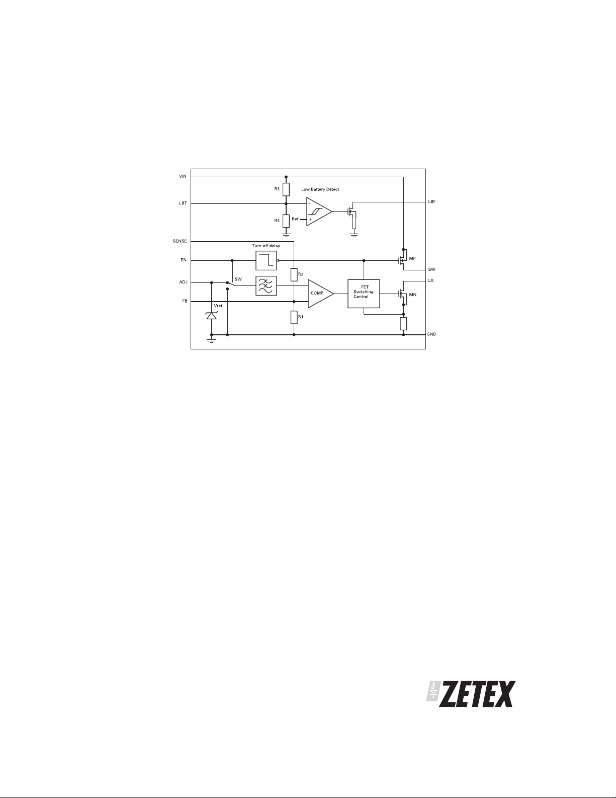
BLOCK DIAGRAM
ZXLB1600
Device description
The device is a flyback boost converter, working in
discontinuous mode.
With reference to the chip block diagram and typical
application circuit, the operation of the device is as
follows:
Control loop
When 'EN' is high, the control circuits become active. The
high side of the coil is connected to the input via a large
PMOSisolatingswitch (MP)and thelow side toground via
NDMOS transistor (MN). The current in the coil is allowed
to build up to an internally defined level (nominally 200 to
300mA) before MN is turned off. The energy stored in the
coil is then transferred to the output capacitor (C2) via
diode(D1). The outputvoltage is sensedat pin 'SENSE' by
internal resistors R1 and R2 (which may be shunted
externallyat pin'FB') and comparedto areference voltage
(1.23V nominal). A comparator senses when the output
voltage is above that set by the reference and its output is
used to control the 'off' time of the output switch. The
control loop is self-oscillating, producing pulses of 10s
maximumduration (switch'on'), at afrequency thatvaries
in proportion to the output load current. The minimum
'off'time of theoutput switch is fixed at1.25s nominal,to
allow time for the coil's energy to be dissipated before the
switch is turned on again. This maintains stable and
efficient operation.
ISSUE 3 - SEPTEMBER 2003
Setting output voltage
With external voltage
The output voltage is equal to the voltage present on
the 'ADJ' pin of the device multiplied by the internal
resistor network factor (R1+R2)/R1. The ADJ pin is
connected to the internal reference voltage of value
V
ADJ(nom)
28V. However, if required, the ADJ pin may be
overdrivenwith anexternal dc voltageV
adjust the output voltage to a value lower than the
default value.
and by default will give a nominal output of
,in orderto
ADJ
5
SEMICONDUCTORS

ZXLB1600
Filtered PWM operation
The input of an internal low pass filter is switched to
V
when the EN pin is high and switched to ground
REF
when the EN pin is low. The output of this filter drives
the comparator within the control loop. A continuous
highstate onENtherefore providesa filteredvoltage of
value Vref to the comparator and the control loop
regulates the output to a nominal value of 28V.
However,by varying the duty cycle (D) of the EN signal
at a suitably high frequency (f>10kHz), the control loop
will see a voltage, that has an average value equal to
the duty cycle multiplied by V
meansof adjusting theoutput voltage toa lower value.
It also allows the device to be both turned on and
adjustedwith a single signalat the 'EN' pin.The output
duringthismode ofoperation willbea dcvoltage equal
to D x 28V
. This provides a
REF
Gated PWM operation
The internal circuitry of the ZXLB1600 is turned off
whenno signal is present on the 'EN' pin formore than
120s (nominal). A low frequency signal applied to the
ENpin willtherefore gate thedevice 'on' and 'off' atthe
gating frequency and the duty cycle of this signal can
be varied to provide a 'chopped' output voltage equal
to D x 28V. For best accuracy, the gating frequency
should be made as low as possible (e.g. below 1kHz),
such that the turn off delay of the chip is only a small
proportion of the gating period.
Low battery detection
A comparator driving an open drain NMOS output
transistor performs the low battery flag function. The
detection threshold (battery voltage falling) is set to
1.98V nominal with internal resistors R3 and R4, but
this can be changed by shunting the internal potential
divider with two external resistors at pin 'LBT'.
Operation is such that the output transistor will be
turned on when the battery voltage falls below the
detection threshold.
V
= 1.21 x (R3+R4)/R4
BLT
A small amount (nominal 20mV) of hysteresis is
provided to aid clean switching. The low battery
detection circuit remains active when 'EN' is low.
Furtherdetails ofsetting outputcurrent aregiven inthe
application notes.
SEMICONDUCTORS
ISSUE 3 - SEPTEMBER 2003
6

ZXLB1600
TYPICAL OPERATING CHARACTERISTICS
(For typical applications circuit at Vin= 3V and TA= 25⬚C unless otherwise stated)
Plot 1 Start-up response at max output voltage 1mA load
Bottom: Enable input (1V/div), Top: Output voltage (10V/div)
Plot 3 Operating waveforms at max output voltage 1mA load
Bottom: LX Output (10V/div), Top: Output voltage (50mV/div ac)
Plot 2 Start-up response at max output voltage 5mA load
Bottom: Enable input (1V/div), Top: Output voltage (10V/div)
Plot 4 Operating waveforms at max output voltage 10mA load
Bottom: LX Output (10V/div), Top: Output voltage (50mV/div ac)
Bottom: Input voltage (1V/div), Top: Output voltage (0.2V/div ac)
Plot 5 Line rejection at 1mA load
ISSUE 3 - SEPTEMBER 2003
Bottom: Load current (1mA/div), Top: Output voltage (0.1V/div ac)
7
Plot 6 Load rejection
SEMICONDUCTORS

ZXLB1600
TYPICAL OPERATING CHARACTERISTICS (Continued)
= 3V and TA= 25⬚C
V
IN
SEMICONDUCTORS
ISSUE 3 - SEPTEMBER 2003
8

TYPICAL OPERATING CHARACTERISTICS (Continued)
= 3V and TA= 25⬚C
V
IN
ZXLB1600
ISSUE 3 - SEPTEMBER 2003
9
SEMICONDUCTORS

ZXLB1600
TYPICAL OPERATING CHARACTERISTICS (Continued)
= 3V and TA= 25⬚C
V
IN
SEMICONDUCTORS
ISSUE 3 - SEPTEMBER 2003
10

APPLICATION NOTES
Adjusting output voltage
When connected as shown in the typical application
circuit, the ZXLB1600 will produce a nominal output
voltageof 28V. Thiscan be adjustedby one ofthe three
methods described below.
ZXLB1600
in this way. However, some non-linearity in the above
expression may occur at values of VADJ below
approximately 0.5V.
Also note that when driving the ADJ pin, the control
voltage must have sufficiently low impedance to sink
the bias current of the internal reference.(10A max).
1) Output voltage adjustment by external resistors
The internal reference and resistor divider network R1
and R2 set a nominal output of 28V. However, this
network is accessible at the FB pin and can be shunted
by means of external resistors to set different nominal
output voltages. The potential divider defines output
voltage according to the relationship:
V
= (R1+R2)/R1 x 1.23V
OUT(dc)
When using external resistors, these should be chosen
with lower values than the internal resistors to
minimize errors caused by the ±25% absolute value
variationof the internalresistors. The internalresistors
have high values in order to minimize these errors.
The following table gives suggested E24/E96 resistor
values for various output voltages.
Required
output
voltage
5V 280k⍀ 91k⍀
12V 715k⍀ 82k⍀
18V 1 M⍀ 75k⍀
20V 1.15 M⍀ 75k⍀
22V 1.15M⍀ 68.1k⍀
25V 1.2 M⍀ 62k⍀
External resistor
across R2
External resistor
across R1
3) PWM output adjustment
A Pulse Width Modulated (PWM) signal can be applied
to the EN pin in order to adjust the output voltage to a
value below the value set in in 1) or 2). This method of
adjustment permits the device to be turned on and the
outputvoltage set bya singlelogic signalapplied tothe
ENpin. No externalresistors or capacitors arerequired
and the amplitude of the control signal is not critical,
providing it conforms to the limits defined in the
electrical characteristics.
Two modes of adjustment are possible as described
below:
Filtered 'DC' mode
If a PWM signal of 10kHz or higher is applied to the EN
pin, the device will remain active when the EN pin is
low. However, the input to the internal low pass filter
willbe switchedalternately fromV
toground, witha
REF
dutycycle (D)corresponding to thatof thePWM signal.
This will present a filtered dc voltage equal to the duty
cycle multiplied by V
to the control loop and will
REF
produce a dc output voltage lower than the maximum
set value. This voltage is given by:
V
= 28 x D
OUT
A square wave signal applied to the EN pin, for
example,willturn thedevice onandproduce anominal
regulated output of 14V.
2) Output adjustment by external voltage
The internal voltage reference (Pin ADJ) may be
overdriven by an external control voltage to set the
output voltage. The relationship between applied
voltage (V
) and output voltage (V
ADJ
V
= 22.86 x V
OUT
ADJ
OUT
) is:
Note that the output can be set to any value between
the input voltage and the maximum operating voltage
ISSUE 3 - SEPTEMBER 2003
11
SEMICONDUCTORS

ZXLB1600
Gated mode
The ZXLB1600 contains a timing circuit that switches
the device on a few microseconds after the application
of a rising edge to EN and turns it back off again
nominally 120s after the falling edge of EN. So, if a
lowerfrequency of1kHz or lessis applied to the ENpin,
the device will be gated on and off at a duty cycle (D)
corresponding to that of the input signal. The average
output voltage is then given by:
V
OUT(avg)
Outputvoltage can be adjustedall the way downto the
input voltage by means of PWM control, but for best
results, the duty cycle range should be kept within the
specified range of 0.4 to 1. Lower duty cycles may
result in increased output ripple and non-linearity in
the relationship between duty cycle and output
voltage. If a greater control range, or reduced ripple is
required,the nominal output canbe adjusted by one of
the other methods before the PWM signal is applied.
Negative output
The ZXLB1600 can be used to provide a negative
output voltage (in addition to the normal positive
output) as shown in the application circuit below. In
this circuit, the external resistors R3 an R4 are used to
set the output voltage to 22V as described in the
previous section. These resistors and output capacitor
~ 28 x D
C2 have relatively low values in this circuit in order to
give a short time constant. This improves the
regulation of the negative voltage.
Capacitor selection
A low ESR ceramic capacitor grounded close to the
GND pin of the package is recommended at the output
of the device. Surface mount types offer the best
performance due to their lower inductance. A
minimum value of 1F is advised, although higher
values will lower switching frequency and improve
efficiency especially at lower load currents. A higher
value will also minimize ripple when using the device
to provide an adjustable dc output voltage.
A good quality, low ESR capacitor should also be used for
inputdecoupling, as the ESRof this capacitor iseffectively
in series with the source impedance and lowers overall
efficiency. This capacitor has to supply the relatively high
peak current to the coil and smooth the current ripple on
the input supply. A minimum value of 3.3F is acceptable
if the input source is close to the device, but higher values
are recommended at lower input voltages, when the
source impedance is high. The input capacitor should be
mounted as close as possible to the IC.
For maximum stability over temperature, capacitors
with X7R dielectric are recommended, as these have a
muchsmallertemperature coefficientthanother types.
SEMICONDUCTORS
ISSUE 3 - SEPTEMBER 2003
12

ZXLB1600
Inductor selection
The choice of inductor will depend on available board
space as well as required performance. Small value
inductors have the advantage of smaller physical size
and may offer lower series resistance and higher
saturation current compared to larger values. A
disadvantage of smaller inductors is that they result in
higher frequency switching, which in turn causes
reduced efficiency due to switch losses. Higher
inductor values can provide better performance at
lower supply voltages. However, if the inductance is
too high, the output power will be limited by the
internal oscillator, which will prevent the coil current
from reaching its peak value. This condition will arise
whenever the ramp time I
(peak) x L/VINexceeds the
LX
preset10µsmaximum ‘on’timelimit fortheLX output.
The ZXLB1600 has been optimized for use with
inductorvalues in therange 10Hto100H.The typical
characteristics show how efficiency and available
output current vary with input voltage and inductance.
The inductor should be mounted as close to the device
as possible with low resistance connections to the LX
and SW pins.
Suitable coils for use with the ZXLB1600 are those in
the LP02506 and DO1608 series, made by Coilcraft.
Diode selection
The rectifier diode (D1) should be a fast low
capacitanceswitching type with lowreverse leakage at
the working voltage. It should also have a peak current
rating above the peak coil current and a continuous
current rating higher than the maximum output load
current. Small schottky diodes such as the BAT54 are
suitable for use with the ZXLB1600 and this diode will
give good all round performance over the output
voltage and current range. At lower output voltages, a
largerschottkydiode suchas theZHCS500or MBR0540
will provide a smaller forward drop and higher
efficiency. At higher output voltages, where forward
drop is less important, a silicon switching diode such
asthe1N4148 canbe used,howeverthis willgive lower
efficiency.
The BAT54S device specified in the application circuit
contains a second diode (D2) as one half of a series
connected pair. This second diode is used here to
clamp possible negative excursions (due to coil
ringing) from driving the drain of the output transistor
below -0.5V. This prevents internal coupling effects,
which might otherwise affect output regulation. The
table below gives some typical characteristics for
various diodes.
Diode Forward voltage at 100mA (V) Peak current
(mA)
BAT54 530 300 200 2
ZHCS500 300 1000 500 15
MBR0540 390 1000 500 1
1N4148 950 450 200 0.025
Continuous current
(mA)
Reverse leakage (µA)
ISSUE 3 - SEPTEMBER 2003
13
SEMICONDUCTORS

ZXLB1600
Increased efficiency
Ifisolation ofthe coilfrom the supply is notneeded, the
high side of this can be connected directly to VIN to
improve efficiency. This prevents power loss in the
internalPMOSswitch andtypical efficiencygainsof 5%
canbe achieved. (See efficiency vs.load curves). Some
applications may require the coil to be fed from a
separate supply with a different voltage to V
case, the SW pin should be left floating.
Layout considerations
PCB tracks should be kept as short as possible to
minimize ground bounce and the ground pin of the
deviceshould be soldered directly tothe ground plane.
It is particularly important to mount the coil and the
input/output capacitors close to the device to minimize
parasitic resistance and inductance, which will
degrade efficiency and increase output ripple. The FB
and LBT pins are high impedance inputs, so PCB track
lengths to these should also be kept as short as
possible to reduce noise pickup. Output ripple is
typically only 50mV p-p, but a small feed-forward
capacitor (~100pF) connected from the FB pin to the
output may help to reduce this further. Capacitance
from the FB pin to ground should be avoided, but a
capacitorcan be connected fromthe LBT pin to ground
toreduce noise pickup into thelow battery comparator
if required.
. In this
IN
Low battery detection circuit
The device contains an independent Low Battery
Detection Circuit that remains powered when the
device is shutdown. The detection threshold is set
internally to a default value of 1.98V, but can be
adjusted by means of external resistors as described
below.
Low battery threshold adjustment, LBT
The internal potential divider network R3/R4 sets the
detection threshold. This is accessible at the LBT pin
and can be shunted by means of external resistors to
set different nominal threshold voltages. The potential
divider defines threshold voltage according to the
relationship:
V
= (R3+R4)/R4 x 1.21V
LBT
When using external resistors, these should be chosen
with lower values than the internal resistors to
minimize errors caused by the ⫾25% absolute value
variationof the internalresistors. The internalresistors
have high values in order to minimize these errors. It is
suggested to use values less than half those shown for
R3, R4 at the bottom of page 3.
Low battery flag output, LBF
Thisisan opendrain outputthatswitches lowwhen the
battery voltage falls below the detection threshold. An
externalpull-up resistor can beconnected to this pin to
allow it to interface to any voltage up to a maximum of
29V.Current in the pull-up resistorshould be limited to
a value below I
BLOL
.
SEMICONDUCTORS
ISSUE 3 - SEPTEMBER 2003
14

Notes:
ZXLB1600
ISSUE 3 - SEPTEMBER 2003
15
SEMICONDUCTORS

ZXLB1600
PACKAGE DIMENSIONSPACKAGE OUTLINE
MILLIMETER INCHES
DIM
MIN. MAX. MIN. MAX.
A ᎏ 1.10 ᎏ 0.43
A1 ᎏ 0.15 ᎏ 0.006
A2 0.75 0.95 0.0295 0.037
D 3.00 BSC 0.118 BSC
E 4.90 BSC 0.1929 BSC
E1 3.00 BSC 0.118 BSC
b 0.17 0.27 0.0066 0.0106
c 0.08 0.23 0.003 0.009
e 0.50 BSC 0.0196 BSC
⍜ 0⬚ 15⬚ 0⬚ 15⬚
L 0.40 0.80 0.015 0.031
L1 0.95 BSC 0.037 BSC
Controlling dimensions are in millimeters. Approximate conversions are given in inches
© Zetex plc 2003
Europe
Zetex plc
Fields New Road
Chadderton
Oldham, OL9 8NP
United Kingdom
Telephone (44) 161 622 4444
Fax: (44) 161 622 4446
hq@zetex.com
These offices are supported by agents and distributors in major countries world-wide.
Thispublicationisissuedtoprovideoutlineinformation only which (unless agreed by the Company in writing) may not be used, applied or reproduced
for any purpose or form part of any order or contract or be regarded as a representation relating to the products or services concerned. The Company
reserves the right to alter without notice the specification, design, price or conditions of supply of any product or service.
For the latest product information, log on to
Zetex GmbH
Streitfeldstraße 19
D-81673 München
Germany
Telefon: (49) 89 45 49 49 0
Fax: (49) 89 45 49 49 49
europe.sales@zetex.com
www.zetex.com
Americas
Zetex Inc
700 Veterans Memorial Hwy
Hauppauge, NY 11788
USA
Telephone: (1) 631 360 2222
Fax: (1) 631 360 8222
usa.sales@zetex.com
Asia Pacific
Zetex (Asia) Ltd
3701-04 Metroplaza Tower 1
Hing Fong Road
Kwai Fong
Hong Kong
Telephone: (852) 26100 611
Fax: (852) 24250 494
asia.sales@zetex.com
ISSUE 3 - SEPTEMBER 2003
SEMICONDUCTORS
16
 Loading...