ZXGD3003E6
5A(peak) gate driver in SOT23-6
General description
The ZXGD3003E6 is a high-speed non-inverting single MOSFET gate driver capable of driving up to 5A
into a MOSFET or IGBT gate capacitive load from supply voltages up to 40V. With typical propagation
delay times down to 2ns and rise/fall times down to 9ns this device ensures rapid switching of the power
MOSFET or IGBT to minimize power losses and distortion in high current fast switching applications.
The ZXGD3003E6 is inherently rugged to latch-up and shoot-through, and its wide supply voltage range
allows full enhancement to minimize on-losses of the power MOSFET or IGBT.
Its low input voltage requirement and high current gain allows high current driving from low voltage
controller ICs, and the optimized pin-out SOT23-6 package with separate source and sink pins eases
board layout, enabling reduced parasitic inductance and independent control of rise and fall slew rates.
Features
• 40V operating voltage range
• 5 amps peak output current
• Fast switching emitter-follower configuration
• 2ns propagation delay time
• 19ns rise/fall time, 1000pF load
• Low input current requirement
• 1.6A(source)/1.4A(sink) output current from 10mA input
• SOT23-6 package
• Separate source and sink outputs for independent control of rise and fall time
• Optimized pin-out to ease board layout and minimize trace inductance
• No Latch Up
• No shoot through
• Near - Zero quiescent and output leakage current
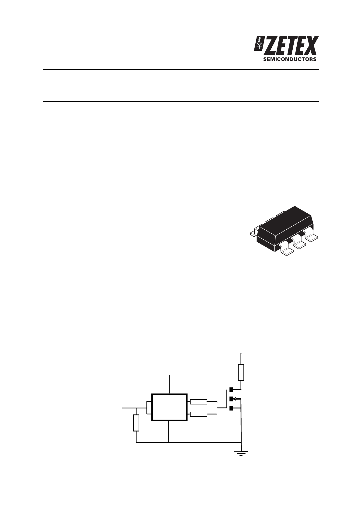
Typical application circuit
V
S
V
CC
V
CC
IN
1
Input
IN
2
ZXGD3003
GND
Issue 2 - October 2007 1 www.zetex.com
© Zetex Semiconductors plc 2007
SOURCE
SINK

Applications
Power MOSFET and IGBT Gate Driving in
• Synchronous switch-mode power supplies
• Secondary side synchronous rectification
• Plasma Display Panel power modules
• 1, 2 and 3-phase motor control circuits
• Audio switching amplifier power output stages
Pin configuration
ZXGD3003E6
V
CC
IN
1
GND
Pin description
Pin Name Pin Function
V
IN
CC
/ IN
1
2
Driver supply
Driver input pins. These are normally connected together by circuit tracks.
GND Ground
SOURCE Source current output.
SINK Sink current output.
Ordering information
Device Reel size
(inches)
Tape width
SOT236
Top view
(mm)
SOURCE
IN
2
SINK
Quantity per
reel
ZXGD3003E6TA 7 8 embossed 3000
Device marking
3003
Issue 2 - October 2007 2 www.zetex.com
© Zetex Semiconductors plc 2007

ZXGD3003E6
Absolute maximum ratings
Parameter Symbol Limit Unit
Supply voltage V
Input voltage V
(c)
(c)
IN1
IN1
+ I
+ I
IN2
=10mA
IN2
=25°C
A
=10mA
(a)
(a)(b)
(a)
Peak sink current
Source current @ I
Sink current @ I
Input current
Power dissipation at T
CC
IN
I
(sink)PK
I
(source)
I
(sink)
I
IN1, IIN2
P
D
Linear derating factor 8.8 mW/°C
Operating and storage temperature range T
, T
j
stg
Thermal resistance
Parameter Symbol Value Unit
Junction to ambient
(a)(b)
R
⍜JC
40 V
40 V
5A
1.6 A
1.4 A
1A
1.1 W
-55 to +150
°C
113 °C/W
NOTES:
(a) For a device surface mounted on 25mm x 25mm x 0.6mm FR4 PCB with high coverage of single sided 1oz copper,
in still air conditions.
(b) For device with two active dice running at equal power.
(c) Pulse width <=300us limit repetition rate to comply with maximum junction temperature.
Issue 2 - October 2007 3 www.zetex.com
© Zetex Semiconductors plc 2007
 Loading...