

VIDEO AMPLIFIER WITH DC RESTORATION
ZXFV4089
DEVICE DESCRIPTION
The ZXFV4089 is a DC restoring circuit and
low-distortion video amplifier. It is specially designed
to provide brightness level stability as a ‘black-level
clamp’ in video systems with very low distortion and
low power consumption.
A high fidelity video amplifier is combined with a
sample-hold switch circuit using an external coupling
capacitor to provide level-shifting of the video output
suchthatatime-gated sampleof thewaveform isset to
be equal to an externalreferencevoltage (usually zero
voltage). A buffered TTL/CMOS logic input signal
controls the switch.
The gain is set externally by two resistors.
Inatypical application,the sample-holdcircuit isgated
on during part ofthe back-porch interval of an analog
video waveform. Then the video waveform is
stabilised for the remainder of the line-scan interval.
ORDERING INFORMATION
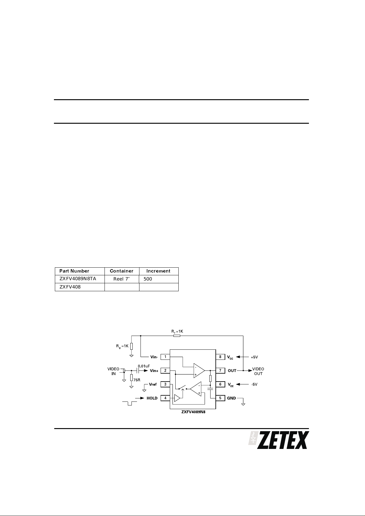
Part Number Container Increment
ZXFV4089N8TA
ZXFV4089N8TC
Reel 7″
Reel 13″
500
2500
FEATURES AND BENEFITS
Various TV systems, PAL, NTSC, SECAM
•
Buffered output using high quality video amplifier
•
Gain is set using two external resistors
•
On chip sample/hold capacitor
•
300 MHz bandwidth
•
0.02% differential gain
•
0.02° differential phase
•
+/-5V supply operation
•
8 mA supply current
•
Pin and function compatible with industry
•
standard part
APPLICATIONS
•
Black Level Clamp, providing stable intensity in
video systems such as
cameras
image capture
video mixing
displays
•
DC restoration of other high frequency signals
CONNECTION DIAGRAM
ADVANCED INFORMATION ISSUE D - SEPTEMBER 2002
1
ZXFV4089
ABSOLUTE MAXIMUM RATINGS
Positive Supply voltage V
Negative Supply Voltage V
Input voltage, pins 1,2,3 to GND V
Output current, pin 7 60mA
Current into Vin and HOLD, pins 2 & 4 5mA
Operating Temperature Range -40⬚C to 85⬚C Storage -65⬚C to +150⬚C
Operating Ambient Junction temperature T
**The thermalresistance from the semiconductordie to ambientistypically 120⬚C/W whentheSO16 package is
mounted on a PCB in free air. The power dissipation of the device when loaded must be designed to keep the
device junction temperature below T
*During power-up and power-down, these voltage ratings require that signals be applied only when the power
supply is connected.
CC to GND
to GND -5.5V to +0.5V
EE
JMAX
JMAX.
ELECTRICAL CHARACTERISTICS
= 5V, VEE= -5V, RFand RG=1k⍀,R
V
CC
PARAMETER CONDITIONS P/C MIN TYP MAX UNIT
DC characteristics
Supply current, holding HOLD = HIGH P 8 10 mA
V
CC
Supply current, sampling HOLD = LOW P 8.5 11 mA
V
CC
Supply current, holding HOLD = HIGH P 8 10 mA
V
EE
Supply current, sampling HOLD = LOW P 8.5 11 mA
V
EE
Amplifier section
Input offset voltage HOLD = HIGH P 1 10 mV
+ input bias current HOLD = HIGH
– input bias current HOLD = HIGH
Transimpedance HOLD = HIGH P 500 1800 K⍀
+ input resistance HOLD = HIGH P 1.5 2 M⍀
Open loop gain HOLD = HIGH P 48 61 dB
Output voltage swing HOLD = HIGH P ±2.5 ±3.0 V
Output drive current HOLD = HIGH P 40 mA
Positive Power Supply Rejection Ratio HOLD = HIGH P 49 57 dB
Negative Power Supply Rejection Ratio HOLD = HIGH P 51 58 dB
Common mode input voltage range HOLD = HIGH C ±3 V
Amplifier output voltage swing HOLD = HIGH P ±2.5 ±3.5 V
Restore section
Composite Input Offset Voltage, from V
to amplifier output
input bias current HOLD = LOW P 3 12 µA
V
REF
Input restore current available, pin 2 HOLD = LOW P 180 300 µA
REF
= 1k, T
LOAD
HOLD = LOW
amb
-0.5V to +5.5V
-0.5V to VCC+0.5V
EE
150⬚C**
=25⬚C unless otherwisestated.
P510
P510
P37mV
µA
µA
TEST - P = 100% production tested, C = characterised
ADVANCED INFORMATION ISSUE D - SEPTEMBER 2002
2
ZXFV4089
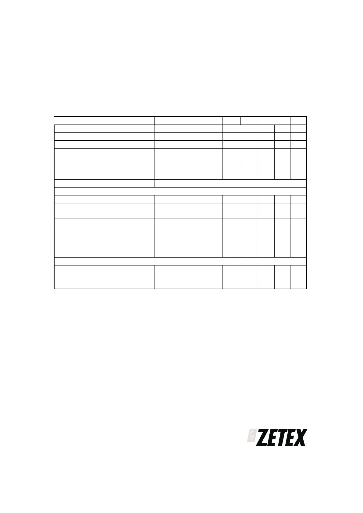
ELECTRICAL CHARACTERISTICS
= 5V, VEE= -5V, RFand RG=1k⍀,R
V
CC
PARAMETER CONDITIONS P/C MIN TYP MAX UNIT
input voltage range HOLD = LOW C ±2 V
V
REF
Positive Power Supply Rejection Ratio HOLD = LOW P 60 90 dB
Negative Power Supply Rejection Ratio HOLD = LOW P 60 90 dB
Logic input HIGH V
Logic input LOW V
Logic input Low current, I
Logic input High current, I
AC characteristics R
Amplifier section
Slew Rate HOLD = HIGH, 2V pk-pk C 400 V/µs
Bandwidth, -3dB HOLD = HIGH C 300 MHz
Bandwidth, ±0.1dB HOLD = HIGH C 100 MHz
Differential Gain, NTSC HOLD = HIGH, f = 3.58 MHz,
Differential Phase, NTSC HOLD = HIGH, f = 3.58 MHz,
Restore section
Slew rate HOLD = LOW C 25 V/µs
Time to enable Hold C 25 ns
Time to disable Hold C 40 ns
Hmin
Lmax
IL
IH
= 1k, T
LOAD
HOLD = LOW P 40 100 µA
HOLD = HIGH P 12 µA
= 1k ohms, R
f=Rg
280mV pk-pk, DC = -714 to
+714 mV
280mV pk-pk, DC = -714 to
+714 mV
=25⬚C unless otherwisestated.
amb
P2V
P 0.8 V
= 150 ohms, C
LOAD
LOAD
C 0.02 %
C 0.02 deg
=10pF
TEST - P = 100% production tested, C = characterised
1. The logic conditions for DC characteristics are: logic LOW = 0.8V max, logic HIGH = 2V min.
ADVANCED INFORMATION ISSUE D - SEPTEMBER 2002
3

ZXFV4089
ZXFV4089DETAILED OPERATING NOTES
Introduction
This device provides a video feed-back amplifier
together with a sample-hold system to allow DC
restoration. TheConnection Diagramon page1 shows
a typical video signal application. No output
termination is shownin the diagram, but if desired the
output can drive a 75 ohm cable via a 75 ohm series
terminating resistor.
Amplifier configuration
The amplifier configuration uses high gain with
feedback in a non-inverting configuration. Two
external resistors are required to set the gain. The
restorationvoltage isset byanexternal reference,Vref,
normally ground. The input signal is applied via an
externalinput couplingcapacitor whichisusedtostore
a DC control level when the sample-hold switch is
open. When the switch is closed, the stored level is
driven to a new value by an external sampling pulse.
DC restoration
HOLD is a TTL input signal which is buffered and
controls the sample-hold switch. A logic LOW state
closes the switch and soenables the feedback control
loop to set the output level equal to Vref (usually
ground). The level of DC shift is maintained when the
logic control returns to the HIGH state and the switch
opens. Inthisway thewholewaveformisconditionally
level shifted, or ‘restored’ to the new DC level.
The sample-hold loop contains the video feed-back
amplifier within its path, and also includes an
additional sample-hold sense amplifier which
compares Vref with the output voltage using an
internal low-pass filter. In the high state, the switch is
open and the average DC level remains fixed apart
from a small drift due to the input bias current of the
amplifier and switch leakage (see below).
Video function
In the video application, the HOLD input state will be
HIGH during the picture line sweep and a
negative-going sampling pulse of typically 1.2 µs
duration will be applied during acentralportionof the
Back Porch interval, so that the Back Porch or ‘Black’
level is clamped to ground. For each line scan, this
gives a brightness level consistent with that of the
original camera signal, despite the AC coupling.
The value of the coupling capacitor affects two main
characteristics of the circuit. Firstly, the available
charging current, together with the capacitor value,
determinesthemaximum DCvoltage correctionwhich
can be applied at each sample. For a charging current
limit of 300 µA applied for 2 µs, the charge injected is
Qmax = 300 µA x 1.2 µs = 360 pC.
Then the maximum voltage shift correction is
Vmax = Qmax/C = 360 pC / 0.01 µF
= 36 mV.
Secondly, in thehold state, the voltage drift is affected
as described below.
Sample-hold drift
In the HOLD state, the drift rate is equal to the
bias/leakage current of about 1 µA divided by the
coupling capacitor value. For a value of 0.01 µF, the
drift rate is then 100 µV/µs. For the typical video line
scan, the switch remains open for the rest of the scan
duration, orabout 62 µs. Thedrift at the endof the line
scan has therefore accumulatedtoabout 6.2 mV. This
will be acceptable for most applications, but if desired
it can be reduced by increasing the value of the
couplingcapacitor. This willresult ina proportionately
smaller value of the maximum available correction
voltage at each scan as described above. Normally,
once settled, the video system requires only a very
small correction at each scan, so this will not present
any problem.
Supply filtering & printed circuit layout
In the applied circuit, the power filtering and printed
layout designneeds special attention as isappropriate
for a high-speed analogcircuit. For each supply lead,
usealeadless ceramicchip capacitor placedvery close
to the device power pin. A value of 0.1µF is
recommended. In addition, a larger value capacitor,
which should be ceramic or solid tantalum
construction, with a value of 1 to 10 µF, is also
recommended for connection to each supply fairly
close to the device.
The layout naturally requires some short
interconnections on the component side (top copper
layer) and a continuous ground plane should be
provided on another layer with plated via holes
providing low inductance ground connections for the
device and other components. The amplifier
frequency responseis affected tosomeextent by stray
capacitance at the inverting input at pin 1. This effect
can be minimised by providing a small cut-out area in
theground planeand otherlayersaround pin1, though
this may not always be necessary for the application.
ADVANCED INFORMATION ISSUE D - SEPTEMBER 2002
4

ZXFV4089
PACKAGE DIMENSIONSPACKAGE OUTLINE
CONTROLLING DIMENSIONS ARE IN INCHES
APPROX IN MILLIMETRES
DIM
INCHES MILLIMETRES
MIN MAX MIN MAX
A 0.053 0.069 1.35 1.75
A1 0.004 0.010 0.10 0.25
D 0.189 0.197 4.80 5.00
H 0.228 0.244 5.80 6.20
E 0.150 0.157 3.80 4.00
L 0.016 0.050 0.40 1.27
e 0.050 BSC 1.27 BSC
b 0.013 0.020 0.33 0.51
c 0.008 0.010 0.19 0.25
⍜ 0⬚ 8⬚ 0⬚ 8⬚
h 0.010 0.020 0.25 0.50
© Zetex plc 2002
Europe
Zetex plc
Fields New Road
Chadderton
Oldham, OL9 8NP
United Kingdom
Telephone (44) 161 622 4422
Fax: (44) 161 622 4420
uksales@zetex.com
These offices are supported by agents and distributors in major countries world-wide.
Thispublication is issued toprovide outlineinformationonlywhich (unless agreed bytheCompanyinwriting) may not beused,appliedor reproduced
for any purposeor form partof any orderor contractor be regardedas a representationrelating to the products orservices concerned. TheCompany
reserves the right to alter without notice the specification, design, price or conditions of supply of any product or service.
For the latest product information, log on to
Zetex GmbH
Streitfeldstraße 19
D-81673 München
Germany
Telefon: (49) 89 45 49 49 0
Fax: (49) 89 45 49 49 49
europe.sales@zetex.com
www.zetex.com
Americas
Zetex Inc
700 Veterans Memorial Hwy
Hauppauge, NY11788
USA
Telephone: (631) 360 2222
Fax: (631) 360 8222
usa.sales@zetex.com
Asia Pacific
Zetex (Asia) Ltd
3701-04 Metroplaza, Tower 1
Hing FongRoad
Kwai Fong
Hong Kong
Telephone: (852) 26100 611
Fax: (852) 24250 494
asia.sales@zetex.com
ADVANCED INFORMATION ISSUE D - SEPTEMBER 2002
5
 Loading...