


SYNC SEPARATOR WITH VARIABLE FILTER
ZXFV401
DEVICE DESCRIPTION
The ZXFV401 provides the ability to separate out video
synchronisation signals for a wide variety of TV and CRT
display systems, standard and non-standard.
Flexibility arises from the use of just three external
resistors to adapt to each application. One resistor
controls a fully integrated internal colour carrier filter
with variable bandwidth. This filter aviods disturbance
from the colour carrier, permitting accurate threshold
slicing for timing extraction.
A second resistor controls the voltage threshold for
loss of signal detection after a time-out interval. The
third resistor controls the timing functions.
DC restoration for displays is facilitated by the Back
Porch synch output, which can be used to drive an
external curcuit to clamp the blanking voltagetoafixed
level.
ORDERING INFORMATION
Part Number Container Increment
ZXFV401N16TA
ZXFV401N16TC
Reel 7″
Reel 13″
CONNECTION DIAGRAM
500
2500
FEATURES AND BENEFITS
PAL, NTSC, SECAM, other TV systems
•
Super accurate synch slice
•
Variable filter for outputs: composite, horizontal,
•
Vertical, back porch, odd / even
No-signal detector
•
On chip sample / hold capacitors
•
+5V single supply
•
4.5 mA supply current
•
Default vertical output where there are no
•
serration pulses
Pin compatible with industry standard part SO16N
•
surface mount package
APPLICATIONS
Digital image capture
•
•
Video input systems requiring separation of
picture timing
•
Video distribution
•
CCTV surveillance
•
Digital multimedia
•
Timing for black level clamp
VIDEO INPUT
C1
0.1uF
75R
0.1uF
PROVISIONAL ISSUE A - FEBRUARY 2002
RFILT
1
RFILT
2
RNOSIG
C2
RNOSIG
3
CSYNC
4
FILTIN
5
VSYNC
6
0VD
7
FILTOUT
8 9
FVIDIN VLEV
1
ZXFV401N16
0VA
HSYNC
V+
ODDFLD
RSET
BKPCH
NOSIG
+5V
COMPOSITE SYNC
16
15
14
13
RSET
12
11
10
HORIZONTAL SYNC
ODD FIELD
BACK PORCH
NO SIGNAL
SYNC TIP VOLTAGE
VERTICAL SYNC
ZXFV401
ABSOLUTE MAXIMUM RATINGS
Supply voltage V
Inputs to ground* -0.5V to VCC+0.5V
Operating Temperature Range -40⬚C to 85⬚C Storage -65⬚C to +150⬚C
Operating Ambient Junction temperature T
**The thermal resistance from the semiconductor die to ambient is typically120⬚C/W when the SO16 package is
mounted on a PCB in free air. The power dissipation of the device when loaded must be designed to keep the
device junction temperature below T
*During power-up and power-down, these voltage ratings require that signals be applied only when the power
supply is connected.
CC
JMAX.
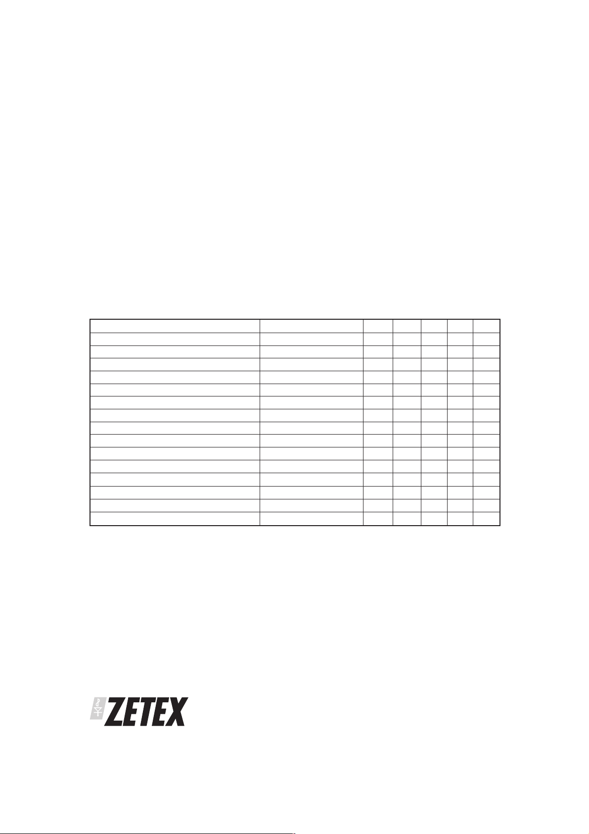
ELECTRICAL CHARACTERISTICS
= 4.75 TO 5.25, R
V
CC
PARAMETER CONDITIONS TEST MIN TYP MAX UNIT
DC Characteristics
Supply current P 4.5 mA
Clamp voltage Pin 4 unloaded P 1.3 1.35 1.8 V
Discharge current at FILTIN Pin 4, Vin = 2V pk-pk C 1 A
Discharge current at FILTIN Pin 4, no signal P 3 6 12 A
Clamp charge current at FILTIN Pin 4, Vin = 1V pk-pk P 2 3 4 mA
Clamp voltage at FVIDIN Pin 8 unloaded P 1.3 1.35 1.8 V
Discharge current at FVIDIN Pin 8, Vin = 2V pk-pk C 1 〈
Discharge current at FVIDIN Pin 8, no signal P 3 6 12 〈
Clamp charge current at FVIDIN Pin 8, Vin = 1V pk-pk P 2 3 4 mA
voltage, pin 12
R
SET
voltage, pin 1
R
FILT
RNOSIG current, pin 2 P 1.5 2.5 3.5 A
Logic output Low voltage, V
Logic output High voltage, V
SET
= 681k, R
OL
OH
FILT
-0.5V to +7V
150⬚C**
JMAX
= 22k, R
IOL= 1.6mA
IOH= 1.6mA
NOSIG
= 82k, T
=25⬚Cunless otherwise stated.
amb
P 1.5 1.75 2 V
P 0.35 0.5 0.65 V
P 0.35 0.8 V
P2.44 V
TEST - P = production tested, C = characterised
PROVISIONAL ISSUE A - FEBRUARY 2002
2

ZXFV401
ELECTRICAL CHARACTERISTICS (CONT)
VCC = 4.75 TO 5.25, R
PARAMETER CONDITIONS TEST MIN TYP MAX UNIT
AC Characteristics
FILTIN function input voltage range PAL/NTSC P 0.4 2 V pk-pk
Filter voltage gain FILTIN to FILOUT P 6 dB
Filter attenuation 4.4MHz for PAL,
Slice level Vin = 1V pk-pk P 40 50 60 %
CSYNC prop. Delay, t
VSYNC delay P 250 ns
VSYNC pulse width, t
VSYNC pulse width, t
VSYNC default delay, t
HSYNC delay P 250 ns
HSYNC pulse width, t
BKPCH delay, t
BKPCH pulse width, t
VLEV output Input 1 Vpk-pk, pin 4 P 500 600 700 mV
NOSIG time-out delay after loss of signal P 600 s
CS
VSYNC
VSYNC
BD
B
SET
VSD
HSYNC
= 681k, R
(PAL)
(NTSC)
= 22k, Tamb = 25 C unless otherwise stated.
FILT
3.6MHz for NTSC
Relative to pin 4 input
Relative to pin 4 input
C12 dB
P 250 400 ns
P 165 s
P 195 s
P273645 s
P 3.8 5 6.2 s
P 250 400 ns
P 2.7 3.7 4.7 s
TEST - P = production tested, C = characterised
PROVISIONAL ISSUE A - FEBRUARY 2002
3
 Loading...