

Zetex ZXFV201N14TA, ZXFV201N14TC Datasheet
QUAD VIDEO AMPLIFIER
Device Description
The ZXFV201 is a quad, high speed amplifier designed for video and
other high speed applications.
It features low differential gain and phase performance. Together
with high output drive and slew rate capability, this brings high
performance to video applications.
Features and Benefits
Unity gain bandwidth 300MHz
·
Slew rate 400V/ s
·
Differential gain 0.01%
·
Differential phase 0.01⬚
·
· Output current 40mA
· Characterized up to 300pF load
· ±5 Volt supply
· Supply current 7mA per amplifier.
· 14 pin SO package
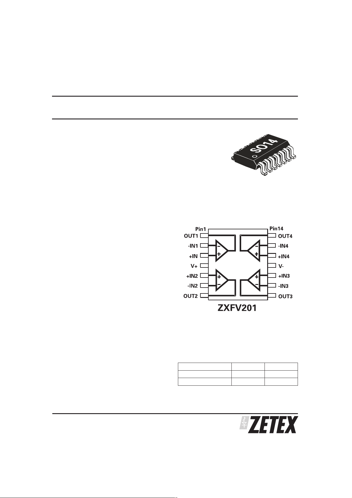
Connection diagram
ZXFV201
Applications
·
Video gain stages
·
CCTV buffer
·
Video distribution
·
RGB buffering
·
xDSL
·
Home theatre
·
Fast ADC signal input drive
·
High frequency instrumentation
·
Cable driving
·
Radar imaging
·
Medical imaging
ISSUE 1 - FEBRUARY 2002
ORDERING INFORMATION
Part Number Container Increment
ZXFV201N14TA reel 7” 500
ZXFV201N14TC reel 13” 2500
1
ZXFV201
ABSOLUTE MAXIMUM RATINGS
Supply Voltage, V+ to V- 11V differential ( 5.5V)
Inputs to ground* V+ - 0.5V to V- - 0.5V
Operating Ambient Temperature Range -40C to 85C Storage -65C to 150C
Operating Junction Temperature T
**The thermal resistance fromthe semiconductor dieto ambient istypically 120⬚C/W when the SO14 package is
mounted on a PCB in free air. The power dissipation of the device when loaded must be designed to keep the
device junction temperature below T
*During power-up and power-down, these voltage ratings require an appropriate sequence of applying and
removing signals and power supplies.
ESD: This device is sensitive to static discharge and proper handling precautions are required.
ELECTRICAL CHARACTERISTICS
±5V power supplies,T
PARAMETER CONDITIONS TEST MIN TYP MAX UNIT
Supply Voltage V+ operating range 4.75 5 5.25 V
Supply Voltage V- operating range -5.25 -5 -4.75 V
Supply current P 23 30 35 mA
Input Common mode voltage range P ⫾3V
Input offset voltage P 1 10 mV
Output offset voltage P 2 20 mV
Input bias current, non-inverting
input
Input resistance P 1.5 2 6.5 M⍀
Open loop gain P 48 61 dB
Output voltage swing P ⫾3V
Output drive current P 40 mA
Positive PSRR P 49 57 dB
Negative PSRR P 51 58 dB
Bandwidth –3dB Av= +1, Vout = 200mV
Bandwidth –0.1dB Av= +1, Vout = 200mV
Slew rate Av= +1
Rise time Vout = ⫾1 V, 10% - 90% C 4.0 ns
Fall time Vout = ⫾1 V, 10% - 90% C 3.2 ns
Propagation delay Vout = ⫾2 V, 50% C 4.0 ns
Differential Gain 3.6MHz(NTSC) and
Differential phase 3.6MHz(NTSC) and
= 25C unless otherwise stated. Rf= 1k⍀,RL= 150⍀, CL<= 10pF
amb
** 150°C
JMAX
.
JMAX
pk-pk
pk-pk
Av=+2
Av = +10
4.4MHz(PAL), R
4.4MHz(PAL), R
= 150⍀
L
= 150⍀
L
P510A
C 300 MHz
C 30 MHz
C 400
400
400
C0.01%
C 0.01 deg
V/s
Test – P = production tested. C = characterised
ISSUE 1 - FEBRUARY 2002
2
 Loading...