

Zetex ZXFBF08W20, ZXFBF08W20TC Datasheet
8 Channel Buffer Device
ZXFBF08
DEVICE DESCRIPTION
The ZXFBF08 is a low cost, high slew rate, octal buffer
amplifier. Built usingtheZetexCA700technology,this
buffer has a small signal bandwidth of greater than
100MHz and a 1 volt pk-pk bandwidth of greater than
20 MHz. Each channel draws only 1.9mA. The device
operates froma ±5 voltsupply, which makes it ideal in
a majority of applications.
This space savingbuffermay be used in awidevariety
of applications such as, video switching matrix,
multi-channel instrumentation equipment, and A/D
input buffer, etc.
FEATURES AND BENEFITS
• 8 Buffers per package
• 100MHz bandwidth
• Low cost
• Low supply current (1.9mA per buffer)
• No thermal runaway
• 20 pin SOIC package
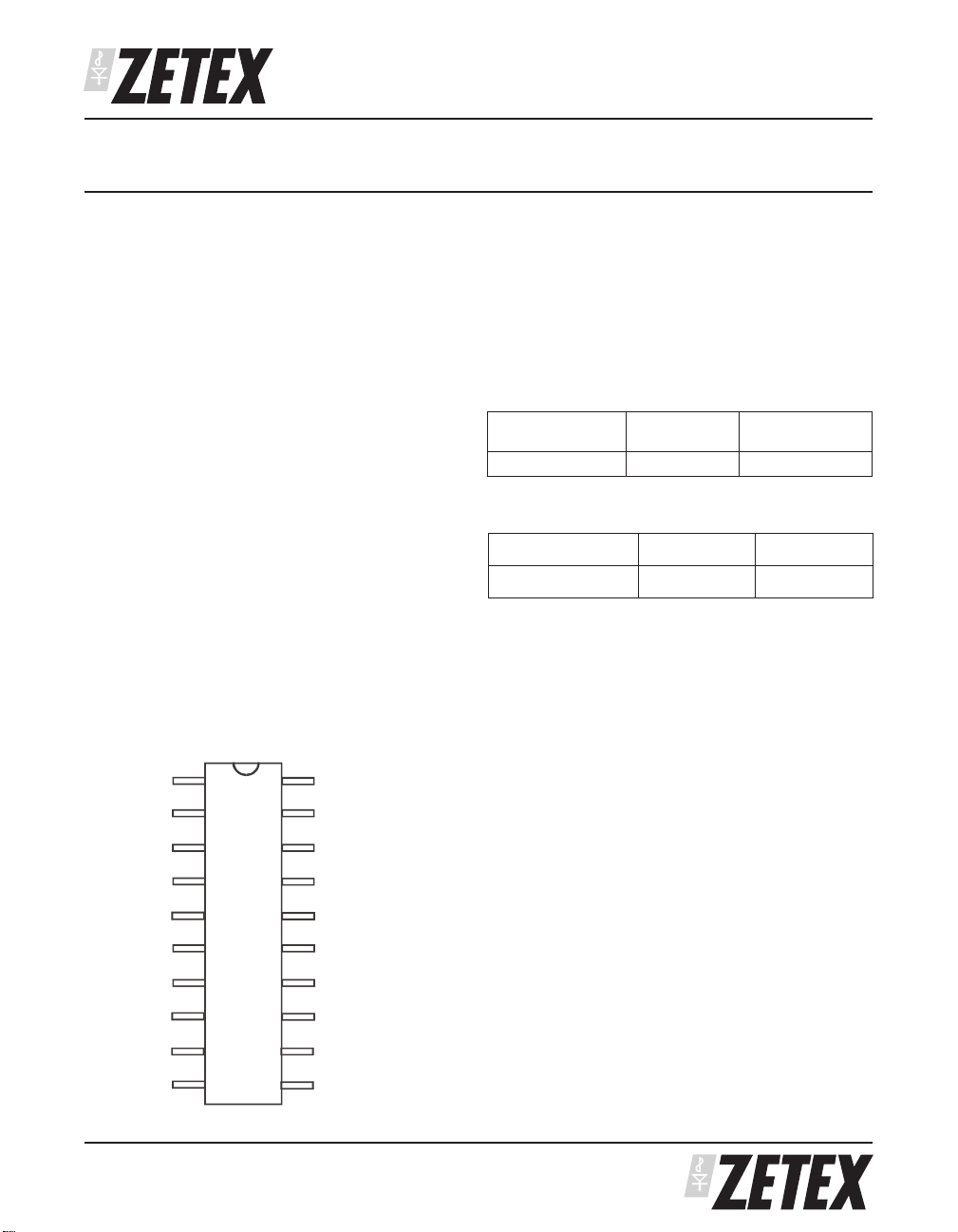
CONNECTION DIAGRAM
OUT1
IN1
1
20
2
19
OUT8
IN8
APPLICATIONS
Video Switching Matrix input buffer
•
Instrumentation
•
Multi-channel A/D input buffer
•
Multi-isolation buffer
•
PART
NUMBER
ZXFBF08W20 SOIC20W ZXFBF08
ORDERING INFORMATION
PART NUMBER CONTAINER INCREMENT
ZXFBF08W20TC Reel 13” 1000
RELATED PRODUCTS
ZXFBF04 4 Channel Buffer
ZXFBF05 4 Channel Buffer with high capacitance
drive
ZXFBF25 4 Channel Buffer with output enable
PACKAGE PART MARK
VOUT2
IN2
OUT3
IN3
V-
3
4
5
6
7
8
OUT4
IN4
ISSUE 2 - OCTOBER 2000
10 11
18
17
16
15
14
13
12
V+
OUT7
IN7
OUT6
IN6
V+
OUT59
IN5
1
ZXFBF08
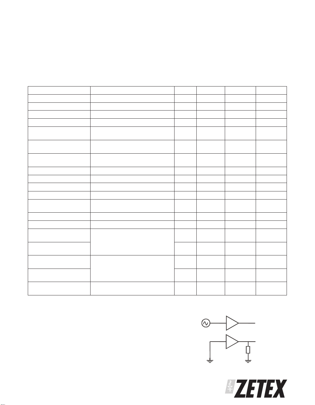
ABSOLUTE MAXIMUM RATINGS
Voltage on any pin 20V (relative to V-)
Operating temperature range 0 to 70°C (de-rated for -40 to 85°C)
Storage Temperature -55 to 125°C
ELECTRICAL CHARACTERISTICS
Test Conditions: Temperature =25°C, V+ = 5.00, V- = -5.00V, RL= 1kΩ, CL= 10pF
Parameter Conditions Min. Typical Max. Units
Offset Voltage V
Offset Voltage Drift V
Supply Current All inputs = 0V 15 25 mA
Input Bias Current V
Output Voltage
DC Gain
DC Gain
Sink Current V
Source Current V
Input Resistance 10 20 100
Output Resistance 5 10 15
Bandwidth 20mVp-p,
Slew Rate 40
Voltage Noise 10 – 100 kHz 15
Differential Gain
NTSC F = 3.58MHz, V
Differential Phase
NTSC
Differential Gain
PAL F = 4.43MHz, V
Differential Phase
PAL
Channel Isolation
= 0V -15 - 15 mV
in
= 0V 20 V/°C
in
= 0V 0.1 0.5 2.0
in
R
=1kΩ
L
= 10kΩ
R
L
= ± 0.5V, RL=1kΩ
V
in
= 0.0V
V
offset
V
= ±0.5V, RL=1kΩ
in
= 0.25V
V
offset
=0V,V
in
in
=0V,V
out
out
0.95 0.98 1.00 V/V
0.95 0.99 1.00 V/V
=0.5V 1.0 2.2 5.0 mA
=-0.5V 6.0 9.0 12.0 mA
±1
±4
100
1.0Vp-p
20
0.1 %
DC ∆V
= 0 to 0.714V
in
0.15 Degrees
= 0.286Vp-p,
in
0.1 %
= 0.286Vp-p,
in
DC ∆V
V
F=4MHz
= 0 to 0.714V
in
= 370mVp-p, RL = 1kΩ
in
0.15 Degrees
-60 dB
µA
V
MΩ
Ω
MHz
V/µs
nV/√Hz
NOTES
Test circuit for measuring channel isolation.
Channel Isolation = 20 x LOG10(V
ISSUE 2 - OCTOBER 2000
out/Vin
)dB
Vin=370mV pk-pk,
F=4MHz
2
V
out
RL = 1kΩ
 Loading...