

ZXCT1030
High-side current monitor with comparator
Description
The ZXCT1030 is a high side current sense
monitor containing an internal reference and
comparator with a non-latching output. Using
this device eliminates the need to disrupt the
ground plane when sensing a load current.
The wide input voltage range of 20V down to as
low as 2.2V make it suitable for a range of
applications. Dynamics and supply current are
optimized for the processing of fast pulses,
associated with switch mode applications.
Features
• Low cost, accurate high-side current sensing
• Output voltage scaling
• Up to 18V output
• 2.2V - 20V supply range
• Voltage reference on chip
• Comparator on chip
• SO8 package
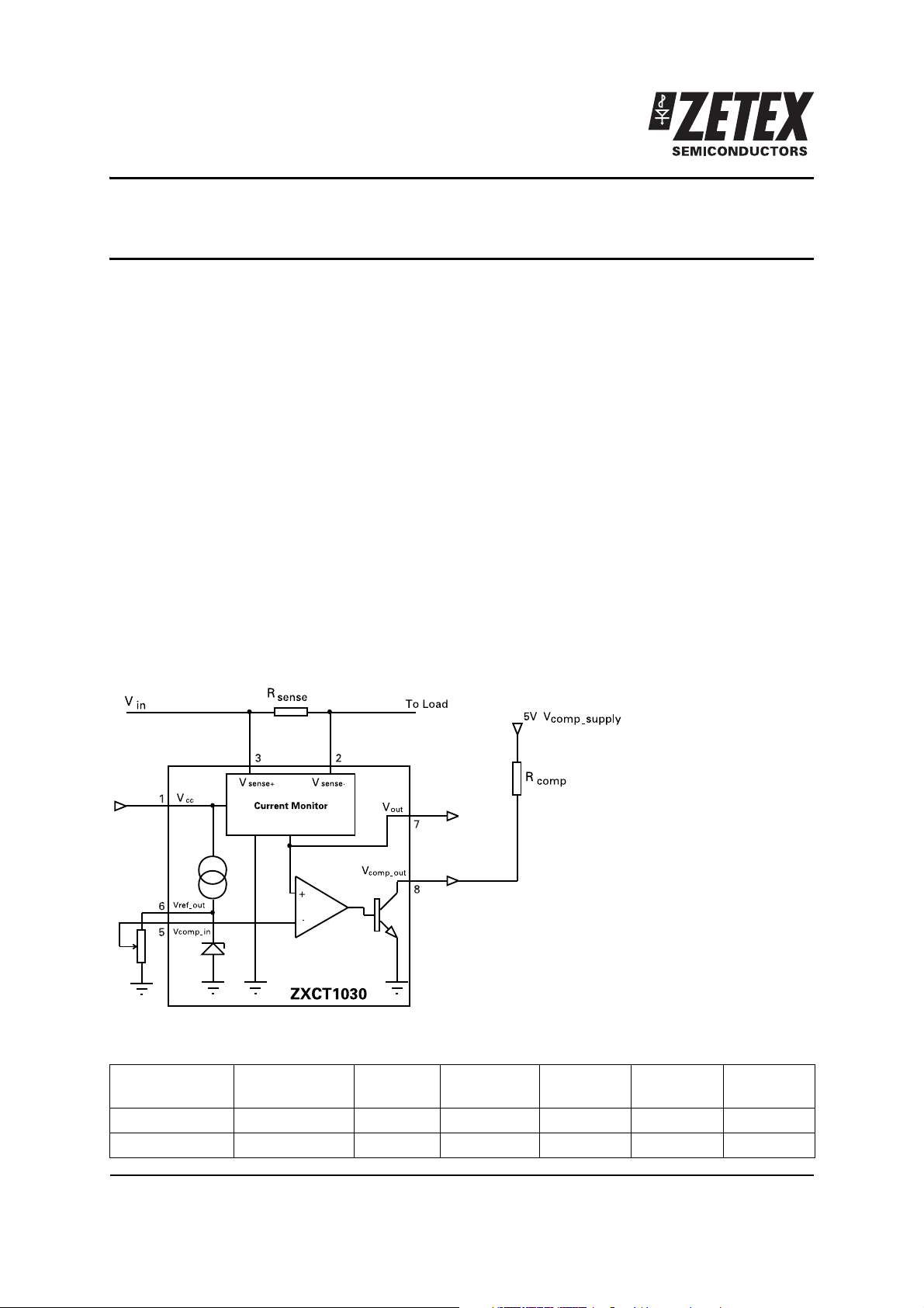
Typical application circuit
Applications
• Battery chargers
• Electronic fuse
•DC motor control
• Over current monitor
• Power management
• Inrush current limiting
Ordering information
Device Status Package Device
marking
ZXCT1030X8TA Last time buy MSOP8 ZXCT1030 7 12 1000
ZXCT1030N8TA
Issue 3 - June 2007 1 www.zetex.com
© Zetex Semiconductors plc 2007
Active SO8 ZXCT1030 7 12 500
Reel size
(inches)
Tape width
(mm)
Quantity
per reel
Absolute maximum ratings
Voltage on any pin -0.6V and V
Operating temperature -40 to 85°C
Storage temperature -55 to 125°C
Package power dissipation (T
amb
= 25°C)
MSOP8 500mW
CC
+0.6V
Recommended operating conditions
Parameter Min. Max. Unit
V
CC
V
SENSE+
V
SENSE
V
OUT
V
comp-in
T
amb
(a)
2.2 20 V
2.2 V
CC
V
10 500 mV
0V
SENSE
-1V V
0.005 10 V
-40 85 °C
Pin-out connections
ZXCT1030
V
SENSE-
V
SENSE+
GND
Pin name Function
V
V
CC
V
comp_out
V
OUT
Vref_out
V
comp_in
CC
V
SENSE-
V
SENSE+
GND Ground
V
comp_in
Supply voltage
Negative sense input
Positive sense input
Comparator input, usually a ratio of the
reference or other control signal
Vref_out Reference output
V
OUT
V
comp_out
Current monitor output voltage
Open collector comparator output
Issue 3 - June 2007 2 www.zetex.com
© Zetex Semiconductors plc 2007
ZXCT1030
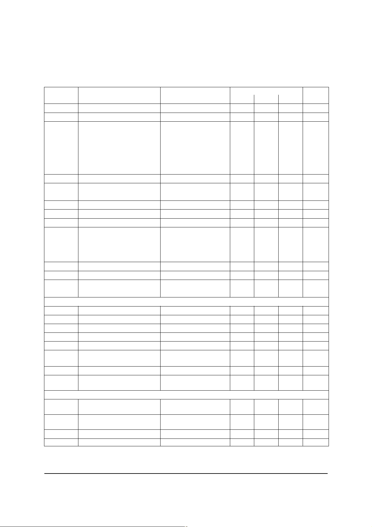
Electrical characteristics (ZXCT1030X8) - Test conditions T
R
comp
= 10kV, V
comp_supply
= 5V unless otherwise stated.
= 25°C, VIN = VCC = 15V,
amb
Symbol Parameter Conditions Limits Unit
Min. Typ. Max.
V
V
CC
V
SENSE+
V
OUT
R
OUT
V
OUT
T
C
I
CC
I
SENSE+
I
SENSE-
V
CM(min)
A
CC
Sense+ range 2.2 VCC
Output voltage V
Output resistance
V
temperature coefficient
Supply current V
V
(b)
Accuracy V
Gain V
BW Bandwidth
range 2.2 20 V
CC
= 0V 0 2 10 mV
SENSE
OUT
SENSE+
V
SENSE-
input current 25 48 90 µA
input current V
Minimum active common
mode voltage
OUT
/V
V
SENSE
V
V
V
V
V
V
VCC =15V 2.8 V
V
V
V
V
V
= 10mV 88 100 112 mV
SENSE
= 30mV 284 300 316 mV
SENSE
= 50mV 480 500 520 mV
SENSE
= 100mV 970 1000 1030 mV
SENSE
= 500mV 4500 5000 5500 mV
SENSE
SENSE-
= 15V, V
OUT
= 1V
1.2 1.5 1.8 k⍀
30 ppm/°C
= 15V 170 270 350 µA
SENSE-
= 14.9V 25 70 220 nA
SENSE-
comp_supply
comp_in
SENSE
SENSE
SENSE
SENSE
SENSE
= 5V
= V
REF
= 10mV
=100mV -3 3 %
= 100mV 9.7 10.0 10.3
=10mVp-p
= 100mVp-p
3 MHz
6 MHz
Comparator
V
comp_in
V
Hysteresis 15 mV
H
Input bias 5 80 150 nA
I
B
Propagation delay 100 ns
T
D
V
Output voltage low 30 150 200 mV
OL
V
OH
Output sink current VOL = 0.4V 2 mA
I
OL
I
OH
Input voltage 0.005 10 V
Output voltage high V
Output high leakage
comp_
supply
V
1.0 µA
current
Voltage reference
V
ref
delta V
Change in V
ref
Isource 5A to
ref
Reference current =
+300
A to -5A
1.200 1.240 1.280 V
10 mV
Isink 300A
T
30 ppm/°C
C
PSR Supply rejection 0.01 %/V
NOTES:
(a) V
(b) Level of V
SENSE
= (V
) - (V
SENSE+
where comparator output defaults to 'off'.
SENSE+
SENSE
-)
Issue 3 - June 2007 3 www.zetex.com
© Zetex Semiconductors plc 2007

ZXCT1030
Electrical characteristics (ZXCT1030N8) - Test conditions T
R
comp
= 10kV, V
comp_supply
= 5V unless otherwise stated.
= 25°C, VIN = VCC = 15V,
amb
Symbol Parameter Conditions Limits Unit
Min. Typ. Max.
V
V
CC
V
SENSE+
V
OUT
R
OUT
V
OUT
T
C
I
CC
I
SENSE+
I
SENSE-
V
CM(min)
A
CC
Sense+ range 2.2 VCC
Output voltage V
Output resistance
V
temperature coefficient
Supply current V
V
(b)
Accuracy V
Gain V
BW Bandwidth
range 2.2 20 V
CC
= 0V 0 2 10 mV
SENSE
OUT
SENSE+
V
SENSE-
input current 48 90 µA
input current V
Minimum active common
mode voltage
OUT
/V
V
SENSE
V
V
V
V
V
V
VCC =15V 2.8 V
V
V
V
V
V
= 10mV 88 100 112 mV
SENSE
= 30mV 284 300 316 mV
SENSE
= 50mV 480 500 520 mV
SENSE
= 100mV 970 1000 1030 mV
SENSE
= 500mV 4500 5000 5500 mV
SENSE
SENSE-
= 15V, V
OUT
= 1V
1.2 1.5 1.8 k⍀
30 ppm/°C
= 15V 170 270 350 µA
SENSE-
= 14.9V 70 220 nA
SENSE-
comp_supply
comp_in
SENSE
SENSE
SENSE
SENSE
SENSE
= 5V
= V
REF
= 10mV
=100mV -3 3 %
= 100mV 9.7 10.0 10.3
=10mVp-p
= 100mVp-p
3 MHz
6 MHz
Comparator
V
comp_in
V
Hysteresis 15 mV
H
Input bias 5 80 150 nA
I
B
Propagation delay 100 ns
T
D
V
Output voltage low 30 150 200 mV
OL
V
OH
Output sink current VOL = 0.4V 2 mA
I
OL
I
OH
Input voltage 0.005 10 V
Output voltage high V
Output high leakage
comp_
supply
V
1.0 µA
current
Voltage reference
V
ref
delta V
Change in V
ref
Isource 5A to
ref
Reference current =
+300
A to -5A
1.200 1.240 1.280 V
10 mV
Isink 300A
T
30 ppm/°C
C
PSR Supply rejection 0.01 %/V
NOTES:
(c) V
(d) Level of V
SENSE
= (V
) - (V
SENSE+
where comparator output defaults to 'off'.
SENSE+
SENSE
-)
Issue 3 - June 2007 4 www.zetex.com
© Zetex Semiconductors plc 2007

Typical characteristics
ZXCT1030
Issue 3 - June 2007 5 www.zetex.com
© Zetex Semiconductors plc 2007

ZXCT1030
Voltage output current monitor
Referring to the block diagram, the current monitor takes the small voltage developed across the
sense resistor (V
referenced signal with a gain of 10. The sense input common mode range is 2.2V to 20V. In this
range, a linear output voltage is delivered.
Reference
The bandgap reference allows the comparator to compare the translated Vsense with threshold
value chosen by the user which can be any voltage from 0 to 1.24V, configured by two external
resistors which forms V
The output current which can be drawn from the comparator reference (I
5µA, making potentiometers ⱖ250k⍀ suitable for setting a threshold level. Where a lower
potentiometer resistor value is used, an additional resistor value should be inserted between V
and VCC to maintain sufficient current for the reference. (as shown in Figure 1).
) and transfers it from the large common mode supply voltage to a ground-
SENSE
comp_in
.
source) is limited to
ref
ref
Figure 1: External resistor for reference level
The voltage reference has a maximum current sink capability. This magnitude of current will be
influenced by the value of R1 which is inserted between V
and VCC. The value of current flowing
ref
through R1 can be expressed as:
I = (V
CC
-V
ref
) / R1
Comparator
The open collector output is active low and is asserted when V
It can be connected to any voltage rail up to Vin via a pull-up resistor. Suggest values for the
resistor are in the range of 10-100k⍀.
In the case where high load currents or a short circuit occurs, thus reducing the common mode
signals (V+, V-) typically below 2.2V, the comparator will default to the asserted state. This can
eliminate a closed loop system 'latch-up' condition, allowing the controller to remove the applied
power.
SENSE
x 10 (V
OUT
) > V
comp_in
.
Stability
To ensure stable operation of the ZXCT1030, it is recommended a decoupling capacitor is placed
across the V
Issue 3 - June 2007 6 www.zetex.com
© Zetex Semiconductors plc 2007
and ground connections. A ceramic 10F will be adequate.
CC

ZXCT1030
Intentionally left blank
Issue 3 - June 2007 7 www.zetex.com
© Zetex Semiconductors plc 2007

Package outline - SO8
ZXCT1030
DIM Inches Millimeters DIM Inches Millimeters
Min. Max. Min. Max. Min. Max. Min. Max.
A 0.053 0.069 1.35 1.75 e 0.050 BSC 1.27 BSC
A1 0.004 0.010 0.10 0.25 b 0.013 0.020 0.33 0.51
D 0.189 0.197 4.80 5.00 c 0.008 0.010 0.19 0.25
H 0.228 0.244 5.80 6.20 ⍜ 0° 8° 0° 8°
E 0.150 0.157 3.80 4.00 h 0.010 0.020 0.25 0.50
L 0.016 0.050 0.40 1.27 - - - - -
Note: Controlling dimensions are in inches. Approximate dimensions are provided in millimeters
Issue 3 - June 2007 8 www.zetex.com
© Zetex Semiconductors plc 2007

Package outline - MSOP8
e
c
E
E1
D
b
A1
A
A2
R1
R
L
DIM Millimeters Inches
Min. Max. Min. Max.
A - 1.10 - 0.0433
A1 0.05 0.15 0.002 0.006
A2 0.75 0.95 0.0295 0.0374
b 0.25 0.40 0.010 0.0157
c 0.13 0.23 0.005 0.009
D 2.90 3.10 0.114 0.122
E 4.90 BSC 0.193 BSC
E1 2.90 3.10 0.114 0.122
e 0.65 BSC 0.025 BSC
L 0.40 0.70 0.0157 0.0192
R 0.07 - 0.0027 -
R1 0.07 - 0.0027 -
Note: Controlling dimensions are in millimeters. Approximate dimensions are provided in inches
ZXCT1030
Issue 3 - June 2007 9 www.zetex.com
© Zetex Semiconductors plc 2007

ZXCT1030
Definitions
Product change
Zetex Semiconductors reserves the right to alter, without notice, specifications, design, price or conditions of supply of any product or
service. Customers are solely responsible for obtaining the latest relevant information before placing orders.
Applications disclaimer
The circuits in this design/application note are offered as design ideas. It is the responsibility of the user to ensure that the circuit is fit for
the user’s application and meets with the user’s requirements. No representation or warranty is given and no liability whatsoever is
assumed by Zetex with respect to the accuracy or use of such information, or infringement of patents or other intellectual property rights
arising from such use or otherwise. Zetex does not assume any legal responsibility or will not be held legally liable (whether in contract,
tort (including negligence), breach of statutory duty, restriction or otherwise) for any damages, loss of profit, business, contract,
opportunity or consequential loss in the use of these circuit applications, under any circumstances.
Life support
Zetex products are specifically not authorized for use as critical components in life support devices or systems without the express written
approval of the Chief Executive Officer of Zetex Semiconductors plc. As used herein:
A. Life support devices or systems are devices or systems which:
1. are intended to implant into the body
or
2. support or sustain life and whose failure to perform when properly used in accordance with instructions for use provided in the
labelling can be reasonably expected to result in significant injury to the user.
B. A critical component is any component in a life support device or system whose failure to perform can be reasonably expected to
cause the failure of the life support device or to affect its safety or effectiveness.
Reproduction
The product specifications contained in this publication are issued to provide outline information only which (unless agreed by the
company in writing) may not be used, applied or reproduced for any purpose or form part of any order or contract or be regarded as a
representation relating to the products or services concerned.
Terms and Conditions
All products are sold subjects to Zetex’ terms and conditions of sale, and this disclaimer (save in the event of a conflict between the two
when the terms of the contract shall prevail) according to region, supplied at the time of order acknowledgement.
For the latest information on technology, delivery terms and conditions and prices, please contact your nearest Zetex sales office.
Quality of product
Zetex is an ISO 9001 and TS16949 certified semiconductor manufacturer.
To ensure quality of service and products we strongly advise the purchase of parts directly from Zetex Semiconductors or one of our
regionally authorized distributors. For a complete listing of authorized distributors please visit: www.zetex.com/salesnetwork
Zetex Semiconductors does not warrant or accept any liability whatsoever in respect of any parts purchased through unauthorized sales channels.
ESD (Electrostatic discharge)
Semiconductor devices are susceptible to damage by ESD. Suitable precautions should be taken when handling and transporting devices.
The possible damage to devices depends on the circumstances of the handling and transporting, and the nature of the device. The extent
of damage can vary from immediate functional or parametric malfunction to degradation of function or performance in use over time.
Devices suspected of being affected should be replaced.
Green compliance
Zetex Semiconductors is committed to environmental excellence in all aspects of its operations which includes meeting or exceeding
regulatory requirements with respect to the use of hazardous substances. Numerous successful programs have been implemented to
reduce the use of hazardous substances and/or emissions.
All Zetex components are compliant with the RoHS directive, and through this it is supporting its customers in their compliance with
WEEE and ELV directives.
Product status key:
“Preview” Future device intended for production at some point. Samples may be available
“Active” Product status recommended for new designs
“Last time buy (LTB)” Device will be discontinued and last time buy period and delivery is in effect
“Not recommended for new designs”
“Obsolete” Production has been discontinued
Datasheet status key:
“Draft version” This term denotes a very early datasheet version and contains highly provisional information, which
“Provisional version” This term denotes a pre-release datasheet. It provides a clear indication of anticipated performance.
“Issue” This term denotes an issued datasheet containing finalized specifications. However, changes to
Zetex sales offices
Europe
Zetex GmbH
Kustermann-park
Balanstraße 59
D-81541 München
Germany
Telefon: (49) 89 45 49 49 0
Fax: (49) 89 45 49 49 49
europe.sales@zetex.com
© 2007 Published by Zetex Semiconductors plc
Device is still in production to support existing designs and production
may change in any manner without notice.
However, changes to the test conditions and specifications may occur, at any time and without notice.
specifications may occur, at any time and without notice.
Americas
Zetex Inc
700 Veterans Memorial Highway
Hauppauge, NY 11788
USA
Telephone: (1) 631 360 2222
Fax: (1) 631 360 8222
usa.sales@zetex.com
Asia Pacific
Zetex (Asia Ltd)
3701-04 Metroplaza Tower 1
Hing Fong Road, Kwai Fong
Hong Kong
Telephone: (852) 26100 611
Fax: (852) 24250 494
asia.sales@zetex.com
Corporate Headquarters
Zetex Semiconductors plc
Zetex Technology Park, Chadderton
Oldham, OL9 9LL
United Kingdom
Telephone: (44) 161 622 4444
Fax: (44) 161 622 4446
hq@zetex.com
Issue 3 - June 2007 10 www.zetex.com
© Zetex Semiconductors plc 2007
 Loading...