

Page 1
ZXCT1011
High-side low drift current monitor
Description
The ZXCT1011 is a high side current sense monitor. Using this type of device eliminates the need
to disrupt the ground plane when sensing a load current.
The ZXCT1011 takes the voltage developed across a current shunt resistor and translates it into a
proportional output current.
A user defined output resistor scales the output current into a ground referenced voltage.
A current reference resistor, external to the IC, results in an improved temperature coefficient
compared to the ZXCT1009.
The wide input voltage range of 20V down to as low as 2.5V make it suitable for a range of
applications. With a minimum operating current of just 4uA, combined with its SOT23-5 package
make it suitable for portable battery equipment too.
Features
■ Accurate high-side current sensing
■ 2.5V to 20V supply range
■ 4 µA quiescent current
■ 1% typical accuracy
■ Package SOT23-5
Applications
■ Automotive current measurement
■ Battery management
■ DC motor and solenoid control
■ Over current monitor
■ Power management
■ Temperature range -40 to 125°C
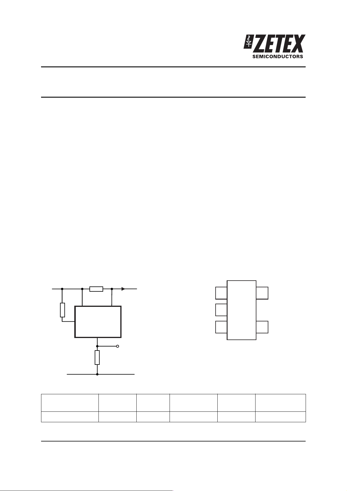
Typical application circuit Pin connections
Vin
R
sense
Load
N/C
R
shunt
120 Ω
GND
5
V
sense+
ZXCT1011
3
I
out
2
V
Rout
4
sense-
I
out
R
shunt
V
V
sense+
V
sense-
Ordering information
Order code Pack Part
mark
ZXCT1011E5TA SOT23-5 1011 7 (180) 8mm 3,000
Issue 1- July 2005 1 www.zetex.com
© Zetex Semiconductors plc 2005
Reel Size
inches (mm)
Tape width Quantity Per
reel
Page 2
Absolute maximum ratings
ZXCT1011
V
sense+
Voltage on any pin 0.6V and V
V
sense+
to V
2.5V
sense-
20 V
sense+
+0.5V
Operating temperature -40 to 125°C
Storage temperature -55 to 150°C
Maximum junction temperature 150°C
Package power dissipation 300mW at T
= 25°C (De-rate to zero at 150°C)
A
Operation above the absolute maximum rating may cause device failure. Operation at the
absolute maximum ratings, for extended periods, may reduce device reliability.
Electrical characteristics
Test conditions TA = 25°C, Vin = 5V, R
Symbol Parameter Conditions Min Typ. Max Units
*
V
in
I
out
V
sense
I
sense -
Supply range - 2.5 - 20 V
Output current V
Sense voltage
V
input current - - - 100 nA
sense-
†
Acc Accuracy R
g
m
Tc
BW
Transconductance
I
out/Vsense
Temperature coefficient
**
Bandwidth V
‡
PSSR Supply rejection V
shunt
sense
= 120⍀. V
= 0V
=10mV
=30mV
=100mV
=200mV
=500mV
=100mV. Unless otherwise stated.
sense
1
84
273
0.97
1.95
4.85
4
116
320
1.00
2.00
5.00
15
124
330
1.03
2.05
5.15
µA
µA
µA
mA
mA
mA
- 0 - 500 mV
= 0.1⍀
sense
V
= 100mV
sense
R
= 120⍀ -10- mA/V
shunt
-3 - 3 %
- - 30 150 ppm/° C
= 10mV
sense
CL = 5pF, R
= 100mV
V
sense
CL = 5pF, R
= 200mV, R
sense
out
out
-400
= 1k⍀
1.5
= 1k⍀
=1k⍀ -68- dB
out
-kHz
MHz
NOTES:
*V
†V
‡ Temperature dependent measurements are extracted from characterization and simulation results.
** Where CL is the capacitance across R
sense+
sense
relative to I
= (V
sense+
out
) - (V
.
sense-
).
.
out
Issue 1- July 2005 2 www.zetex.com
© Zetex Semiconductors plc 2005
Page 3
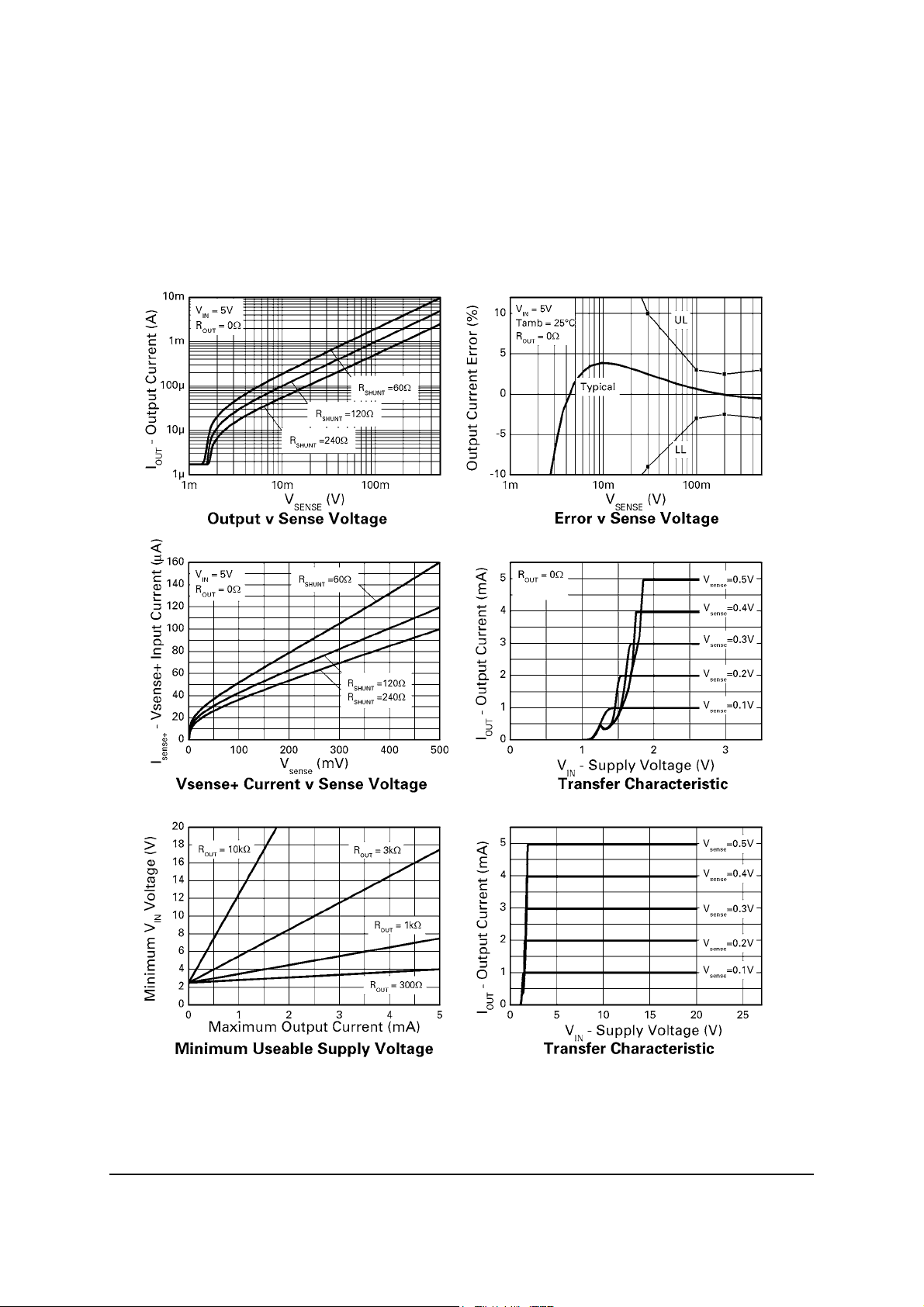
Typical characteristics
ZXCT1011
TA=25°C, R
= 120 unless otherwise stated.
shunt
Issue 1- July 2005 3 www.zetex.com
© Zetex Semiconductors plc 2005
Page 4

Typical characteristics
ZXCT1011
TA=25°C, R
= 120 unless otherwise stated.
shunt
Issue 1- July 2005 4 www.zetex.com
© Zetex Semiconductors plc 2005
Page 5

Pin description
Pin no. Pin name Pin function
1 N/C No connection
ZXCT1011
2I
3R
4V
out
shunt
sense-
Output current - follows transconductance of sense voltage gm = 10mA/V
for R
shunt
=120⍀
Trimming resistor Input. - used to trim gain value 60⍀ ⱕ R
Low side current sense input. – connect to load/battery etc. Must be
lower than V
for correct operation. Cannot be grounded
sense+
without additional series resistor.
5V
sense+
High side current sense input. – Connect to supply rail. Must be
higher than V
for correct operation.
sense+
Application information
Design example
The following lines describe how to scale a load current to an output voltage.
V
= (V
sense
Defining then I
= Iq + V
out
since gm= 1.2 / R
I
= Iq + [ (V
out
= Iq + [ (1.2 x I
sense+
sense
shunt
) - (V
x g
sense
sense-
m
x 1.2) / R
x R
load
) = I
shunt
sense
load
/ R
]
shunt
x R
sense
) ]
shunt
ⱕ 240⍀
Note: Iq is embedded into the specification of the ZXCT1011 and therefore appears an offset error.
∴ V
= (R
out
out
x I
) + [(1.2 x R
offset
out
x I
load
x R
sense
) / R
shunt
]
The output current of the ZXCT1011 is directly related to the size of the trimming resistor used. It
is important to ensure the tolerance of R
is considered. A 1% change in R
shunt
will cause a
shunt
1% change in output.
Consider the following: -
Issue 1- July 2005 5 www.zetex.com
© Zetex Semiconductors plc 2005
Page 6

ZXCT1011
A 1 ampere load current is to be measured into a battery. The output signal required to an over
current controller needs to be 3.3V. What is a suitable value of R
to the supply current be?
V
= 5.0V - 9.0V
in
I
= 1.0A
load
Output signal required: 3.3V
V
= 5.0V - 9.0V
in
R
120R
shunt
R
sense
I
= 1A
5
V
sense+
3
R
shunt
ZXCT
1011
I
out
4
V
sense-
2
load
R
load
3.3V
and what will the error due
out
R
out
Figure 1 ZXCT1011 to measure a 1.0 A load current
To obtain the highest accuracy, choose the of R
R
= 0.1/1.0 = 0.1⍀
sense
to give 100mV:
sense
The transconductance using a 120⍀ resistor will be 10mA/V.
Choose R
to give V
out
= 3.3V, when V
out
sense
= 100mV
Rearranging equation 1 without the offset error gives:
R
out
R
out
= (V
= 3.3k⍀
out
x R
shunt
) / (1.2 x I
Now consider the offset error for this resistor:
Load
x R
sense
)
Offset due to supply current = R
x 4x10⁻⁶µA = 13.2mV = 0.4%
out
Issue 1- July 2005 6 www.zetex.com
© Zetex Semiconductors plc 2005
Page 7

ZXCT1011
Application information (cont.)
Minimum operating voltage
The minimum operating voltage of the ZXCT1011 is 2.5V and is defined as the difference between
V
the device when considering R
R
sense+
V
in
shunt
120R
and the I
= 10V
pin. It must be ensured that sufficient headroom is given for the operation of
out
R
sense
5
V
sense+
3
R
shunt
V
ZXCT
1011
I
out
2
sense-
4
out
.
loadTo
R
V
out
3.3K
Figure 2 Considerations for supply rail
Voltage across device 2.5V
V
- V
out
2.5V
= I
out
out
x R
out
in
Where V
At low supply voltages and high Vsense measurements, special care must be taken to ensure the
correct operation.
The circuit in figure 2.0 shows a ZXCT1011 operating from 10V supply rail. The minimum
operating voltage of the ZXCT1011 is 2.5V. This allows a maximum output voltage of 7.5V to be
set at V
. A 3k resistor on the output would draw a maximum 2.5mA from Iout. - See minimum
out
usable supply voltage graph on page 4.
Issue 1- July 2005 7 www.zetex.com
© Zetex Semiconductors plc 2005
Page 8

Packaging details - SOT23-5
ZXCT1011
Europe
Zetex GmbH
Streitfeldstraße 19
D-81673 München
Germany
Telefon: (49) 89 45 49 49 0
Fax: (49) 89 45 49 49 49
europe.sales@zetex.com
These offices are supported by agents and distributors in major countries world-wide.
This publication is issued to provide outline information only which (unless agreed by the company in writing) may not be used, applied
or reproduced for any purpose or form part of any order or contact or be regarded as a representation relating to the products or services
concerned. The company reserves the right to alter without notice the specification, design, price or conditions of supply of any product or
service.
Americas
Zetex Inc
700 Veterans Memorial Highway
Hauppauge, NY 11788
USA
Telephone: (1) 631 360 2222
Fax: (1) 631 360 8222
usa.sales@zetex.com
Asia Pacific
Zetex (Asia Ltd)
3701-04 Metroplaza Tower 1
Hing Fong Road, Kwai Fong
Hong Kong
Telephone: (852) 26100 611
Fax: (852) 24250 494
asia.sales@zetex.com
Corporate Headquarters
Zetex Semiconductors plc
Zetex Technology Park, Chadderton
Oldham, OL9 9LL
United Kingdom
Telephone (44) 161 622 4444
Fax: (44) 161 622 4446
hq@zetex.com
Issue 1- July 2005 8 www.zetex.com
© Zetex Semiconductors plc 2005
 Loading...