

ENHANCED HIGH-SIDE CURRENT MONITOR
ZXCT1010
DESCRIPTION
The ZXCT1010 is a high side current sense monitor.
Using this device eliminates the need to disrupt the
ground plane when sensing a load current.
It is an enhanced version of the ZXCT1009 offering
reduced typical output offset and improved accuracy
at low sense voltage.
Thewideinputvoltage rangeof 20Vdown toas lowas
2.5V make it suitable for a range of applications. A
minimum operating current of just 4µA, combined
with its SOT23-5 package make suitable for portable
battery equipment.
FEATURES
• Low cost, accurate high-side current sensing.
• Output voltage scaling.
• Up to 2.5V sense voltage.
• 2.5V – 20V supply range.
• 300nA typical offset current.
• 3.5µA quiescent current.
• 1% typical accuracy.
•
SOT23 -5 package.
APPLICATIONS
Battery Chargers
•
Smart Battery Packs
•
DC Motor control
•
Over current monitor
•
Power Management
•
Programmable current source
•
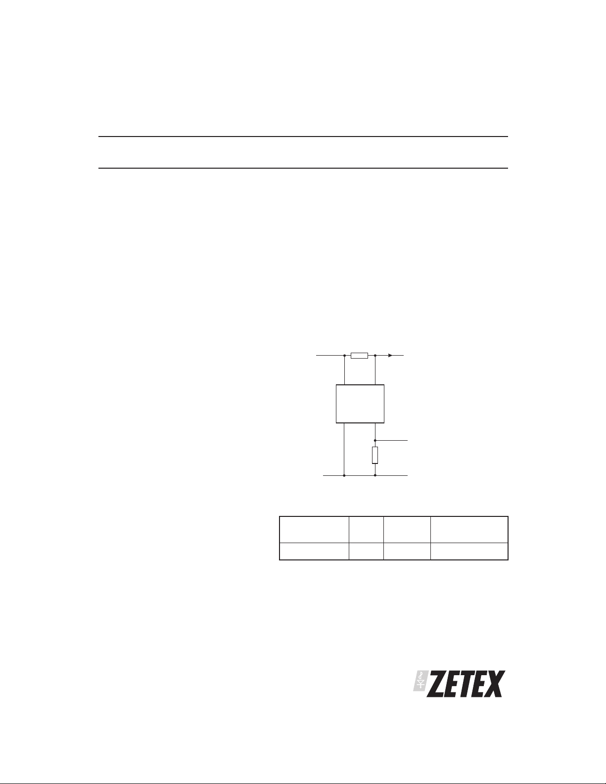
APPLICATION CIRCUIT
V
in
R
sense
V
in
ZXCT1010
GND
Load
I
out
R
out
To Load
V
out
ISSUE 8 - JANUARY 2004
ORDERING INFORMATION
DEVICE REEL
ZXCT1010E5TA 7” 8mm 3,000 units
PARTMARK 101
PACKAGE SOT23-5
1
SIZE
TAPE
WIDTH
QUANTITY PER
REEL
SEMICONDUCTORS
ZXCT1010
ABSOLUTE MAXIMUM RATINGS
Voltage on any pin -0.6V to 20V (relative to GND)
Continuous output current 25mA
Continuous sense voltage V
+ 0.5V > V
in
Operating Temperature -40 to 85°C
Storage Temperature -55 to 150°C
Package Power Dissipation (T
= 25°C)
A
SOT23-5 500mW
ELECTRICAL CHARACTERISTICS
Test Conditions TA= 25°C, Vin= 5V, R
SYMBOL PARAMETER CONDITIONS LIMITS UNIT
V
in
I
out
I
q
V
sense
I
sense
1
VCCRange 2.5 20 V
Output current V
Ground pin current V
2
Sense Voltage 0 2500 mV
Load pin
input current
Acc Accuracy
Gm Transconductance,
I
out/Vsense
BW Bandwidth RF P
1
Includes input offset voltage contribution
2
V
sense=Vin-Vload
3
-20dBm=63mVp-p into 50Ω
out
V
V
V
V
R
V
V
V
= 100Ω.
=0V
sense
= 10mV
sense
= 100mV
sense
= 200mV
sense
=1V
sense
= 0V 3.5 8 µA
sense
= 0.1Ω
sense
= 200mV
sense
= -20dBm
in
= 10mV dc
sense
= 100mV dc
sense
sense
†
> Vin– 5V
Min Typ Max
0
85
0.975
1.95
9.7
0.3
100
1.00
2.00
10.0
-2.5 2.5 %
10000 µA/V
3
300
2
10
115
1.025
2.05
10.3
µA
µA
mA
mA
mA
100 nA
kHz
MHz
SEMICONDUCTORS
ISSUE 8 - JANUARY 2004
2
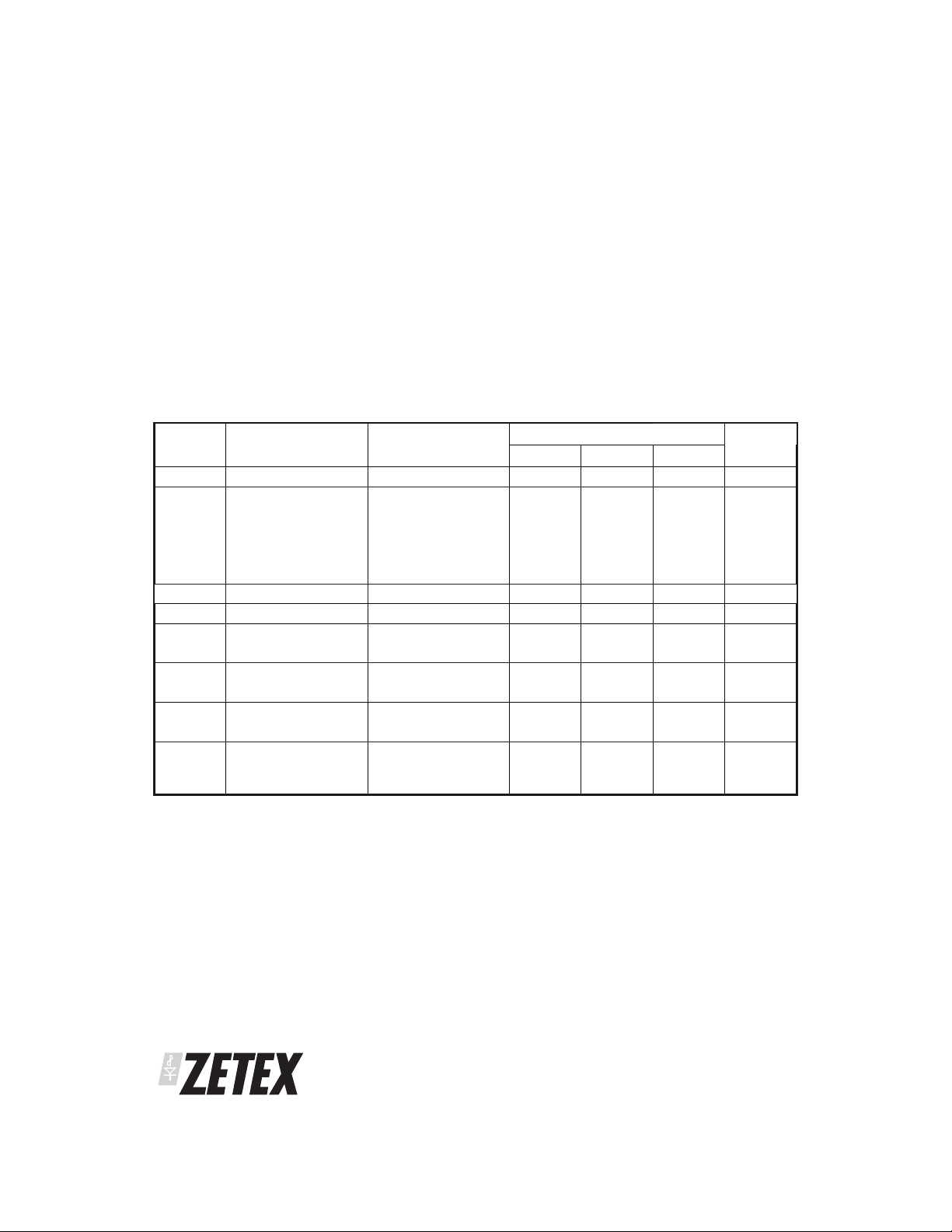
TYPICAL CHARACTERISTICS
ZXCT1010
ISSUE 8 - JANUARY 2004
3
SEMICONDUCTORS

ZXCT1010
PIN DESCRIPTION
Pin Name Pin Function
V
in
Load Connection to load/battery
I
out
GND Ground
CONNECTION DIAGRAM
SOT23-5
Package Suffix – E5
Supply Voltage
Output current, proportional to Vin-V
load
NC
GND
I
out
1
2
3
5
4
Top View
SCHEMATIC DIAGRAM
V
in
100Ω
Load
V
IN
Load
+
-
I
out
SEMICONDUCTORS
ISSUE 8 - JANUARY 2004
4

ZXCT1010
POWER DISSIPATION
The maximum allowable power dissipation of the
device for normal operation (Pmax), is a function of
the package junction to ambient thermal resistance
(θja), maximum junction temperature (Tjmax), and
ambient temperature (Tamb), according to the
expression:
P
max
= (Tj
max
– T
amb
) / θ
ja
The device power dissipation, PDis given by the
expression:
P
D=Iout
.(Vin-V
) Watts
out
APPLICATIONS INFORMATION
The following lines describe how to scale a load
current to an output voltage.
= Vin-V
V
V
out
sense
= 0.01 x V
sense
load
x R
out
1
E.g.
A 1A current is tobe represented by a 100mV output
voltage:
1)Choose the value of R
to give 50mV > V
sense
sense
500mV at full load.
For example V
= 100mV at 1.0A. R
sense
sense
= 0.1/1.0
=> 0.1 ohms.
2)Choose R
to give V
out
= 100mV, when V
out
sense
100mV.
/(V
1
for R
sense
gives:
out
x 0.01)
Rearranging
R
out=Vout
= 0.1 / (0.1 x 0.01) = 100 Ω
R
out
TYPICAL CIRCUIT APPLICATION
V
in
R
sense
>
=
ISSUE 8 - JANUARY 2004
Load
V
in
ZXCT1010
I
out
V
out
R
out
R
load
Where R
GND
represents any load including DC motors,
load
a charging battery or further circuitry that requires
monitoring, R
can be selected on specific
sense
requirements of accuracy, size and power rating.
5
SEMICONDUCTORS

ZXCT1010
APPLICATIONS INFORMATION (Continued)
1kΩ
10µH
220Ω
140µH
ZHCS1000
0.2Ω
V
in
100Ω
ZXCT1010
I
out
100Ω
Load
-
+
Charger Input To Battery +
BC81725
5V
bq2954
support components omitted for clarity
FZT789A
BAS16
MOD pin
FMMT451
SNS pin
Li-Ion Charger Circuit
The above figure shows the ZXCT1010 supporting
the Benchmarq bq2954 Charge Management IC.
Most of the support components for the bq2954 are
omitted for clarity. This design also uses the Zetex
FZT789A high current Super- PNP as the switching
transistor in the DC-DC step down converter and the
FMMT451 as the drive NPN for the FZT789A. The
circuit can be configured to charge up to four Li-Ion
cells at a charge current of 1.25A. Charge can be
terminated on maximum voltage, selectable
minimum current, or maximum time out. Switching
frequencyofthe PWMloopis approximately 120kHz.
Bi-Directional Current Sensing
The ZXCT1010 can be used to measure current
bi-directionally, if two devices are connected as
shown below.
3
Iout
4
Load5Vin
V
1
R
sense
4
Load
Vin
5
Iout
3
R
out
V
2
V
out
If the voltage V1 is positive with respect to the
voltageV2 the lowerdevice willbeactive, delivering
a proportional output current to Rout. Due to the
polarity of the voltage across Rsense, the upper
device will be inactive and will not contribute to the
current delivered to Rout. When V2 is more positive
than V1, current will be flowing in the opposite
direction, causing the upper device to be active
instead.
Non-linearity will be apparent at small values of
Vsense due to offset current contribution. Devices
can use separate output resistors if the current
direction is to be monitored independently.
Bi-directional Transfer Function
SEMICONDUCTORS
5
4
3
2
1
Output Current (mA)
0
-400 -200 0 200 400
Sense Voltage (mV)
Output Current v Sense Voltage
6
ISSUE 8 - JANUARY 2004

APPLICATIONS INFORMATION (Continued)
PCB trace shunt resistor for low cost
solution.
Thefigure below showsoutput characteristics of the
device when using a PCB resistive trace for a low
cost solution in replacement for a conventional
shunt resistor. The graph shows the linear rise in
voltage across the resistor due to the PTC of the
material and demonstrates how this rise in
resistance value over temperature compensates for
the NTC of the device.
Thefigure opposite shows a PCB layout suggestion.
The resistor section is 25mm x 0.25mm giving
approximately 150mΩ using 1oz copper. The data
for the normalised graph was obtained using a 1A
load current and a 100Ω output resistor. An
electronic version of the PCB layout is available at
www.zetex.com/isense
ZXCT1010
Actual Size
Layout shows area of shunt
resistor compared to SOT23-5
package. Not actual size
ISSUE 8 - JANUARY 2004
7
SEMICONDUCTORS
ZXCT1010
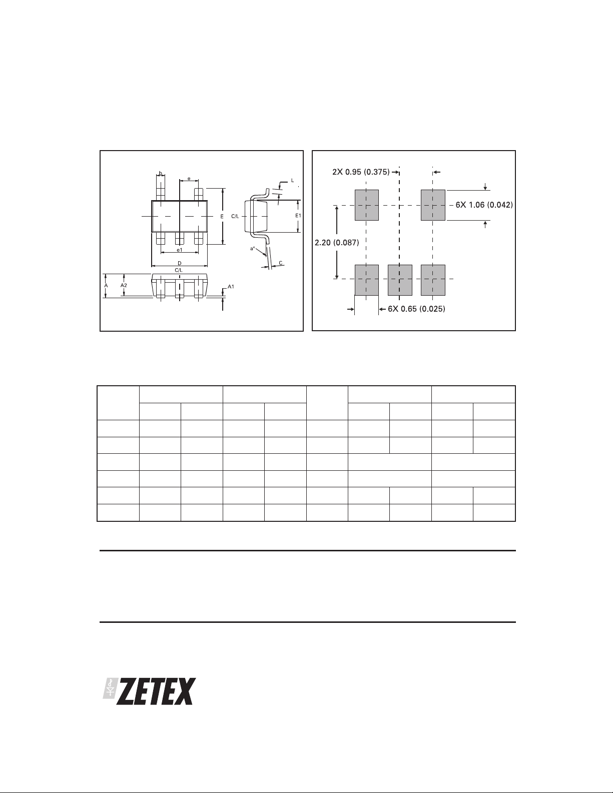
PACKAGE DIMENSIONS
PAD LAYOUT DETAILS
Controlling dimensions are in millimeters. Approximate conversions are given in inches
PACKAGE DIMENSIONS
DIM Millimetres Inches DIM Millimetres Inches
MIN MAX MIN MAX MIN MAX MIN MAX
A 0.90 1.45 0.035 0.057 E 2.60 3.00 0.102 0.118
A1 0.00 0.15 0.00 0.006 E1 1.50 1.75 0.059 0.069
A2 0.90 1.3 0.035 0.051 e 0.95 REF 0.037 REF
b 0.35 0.50 0.014 0.020 e1 1.90 REF 0.075 REF
C 0.09 0.20 0.0035 0.008 L 0.10 0.60 0.004 0.024
D 2.80 3.00 0.110 0.118 a° 0 10 0 10
© Zetex plc 2003
Europe
Zetex plc
Fields New Road
Chadderton
Oldham, OL9 8NP
United Kingdom
Telephone (44) 161 622 4444
Fax: (44) 161 622 4446
hq@zetex.com
These offices are supported by agents and distributors in major countries world-wide.
Thispublicationisissuedtoprovideoutlineinformationonlywhich(unless agreed by the Company in writing) may not be used,appliedorreproduced
for any purpose or form part of any order or contract or be regarded as a representation relating to the products or services concerned. TheCompany
reserves the right to alter without notice the specification, design, price or conditions of supply of any product or service.
For the latest product information, log on to
Zetex GmbH
Streitfeldstraße 19
D-81673 München
Germany
Telefon: (49) 89 45 49 49 0
Fax: (49) 89 45 49 49 49
europe.sales@zetex.com
www.zetex.com
Americas
Zetex Inc
700 Veterans Memorial Hwy
Hauppauge, NY 11788
USA
Telephone: (1) 631 360 2222
Fax: (1) 631 360 8222
usa.sales@zetex.com
Asia Pacific
Zetex (Asia) Ltd
3701-04 Metroplaza Tower 1
Hing Fong Road
Kwai Fong
Hong Kong
Telephone: (852) 26100 611
Fax: (852) 24250 494
asia.sales@zetex.com
ISSUE 8 - JANUARY 2004
SEMICONDUCTORS
8
 Loading...