

ZETEX ZXCT1009 Technical data
HIGH-SIDE CURRENT MONITOR
ZXCT1009
DESCRIPTION
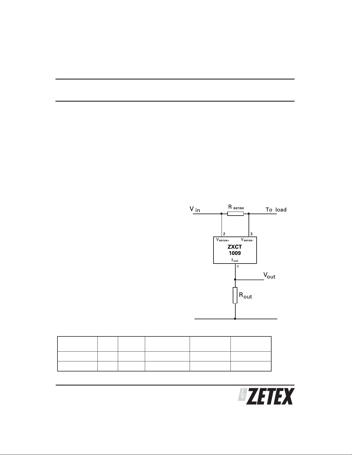
The ZXCT1009 is a high side current sense monitor.
Using this device eliminates the need to disrupt the
ground plane when sensing a load current.
It takes a high side voltage developed across a current
shunt resistor and translates it into a proportional
output current.
A user definedoutput resistor scales the output current
into a ground-referenced voltage.
The wide input voltage range of 20V down to as low as
2.5V make it suitable for a range of applications. A
minimum operating current of just4A,combinedwith
its SOT23 package make it a unique solution for
portable battery equipment.
FEATURES
Low cost, accurate high-side current sensing
•
Output voltage scaling
•
•
Up to 2.5V sense voltage
•
2.5V – 20V supply range
•
4µA quiescent current
•
1% typical accuracy
•
SOT23 and SM8 packages
APPLICATIONS
Battery chargers
•
Smart battery packs
•
DC motor control
•
Over current monitor
•
Power management
•
Level translating
•
Programmable current source
•
APPLICATION CIRCUIT
ORDERING INFORMATION
DEVICE REEL
ZXCT1009FTA 7” 8mm 3,000 units 109 SOT23
ZXCT1009T8TA 7” 12mm 1,000 units ZXCT1009 SM8
ISSUE 9 - OCTOBER 2005
SIZE
TAPE
WIDTH
QUANTITY PER
REEL
1
PARTMARKING PACKAGE
SEMICONDUCTORS
ZXCT1009
ABSOLUTE MAXIMUM RATINGS
Voltage on any pin -0.6V to 20V (relative to I
Continuous output current 25mA
Continuous sense voltage V
in
+ 0.5V > V
sense
†
Operating temperature -40 to 85°C
Storage temperature -55 to 125°C
Package power dissipation (T
= 25°C)
A
SOT23 450mW - derate to zero at 125°C
SM8 2W
Operation above the absolute maximum rating may cause device failure. Operation at the absolute maximum
ratings for extended periods may reduce device reliability.
ELECTRICAL CHARACTERISTICS
Test Conditions TA= 25°C, Vin= 5V, R
SYMBOL PARAMETER CONDITIONS LIMITS UNIT
V
in
1
I
out
V
sense
I
sense
Acc Accuracy
Gm Transconductance,
BW Bandwidth RF Pin= -20dBm‡
1
Includes input offset voltage contribution
†
V
sense=Vin-Vload
‡ -20dBm=63mVp-p into 50Ω
VCCrange 2.5 20 V
Output current V
†
Sense voltage 0 2500 mV
-V
input current
I
-
sense
out/Vsense
out
V
V
V
V
R
V
V
V
= 100Ω.
sense
sense
sense
sense
sense
sense
sense
sense
sense
=0V
=10mV
=100mV
=200mV
=1V
=0.1Ω
=200mV
= 10mV dc
= 100mV dc
Min Typ Max
1
90
0.975
1.95
9.6
-2.5 2.5 %
)
out
> Vin– 5V
4
104
1.002
2.0
9.98
10000 µA/V
300
2
15
120
1.025
2.05
10.2
100 nA
µA
µA
mA
mA
mA
kHz
MHz
SEMICONDUCTORS
ISSUE 9 - OCTOBER 2005
2
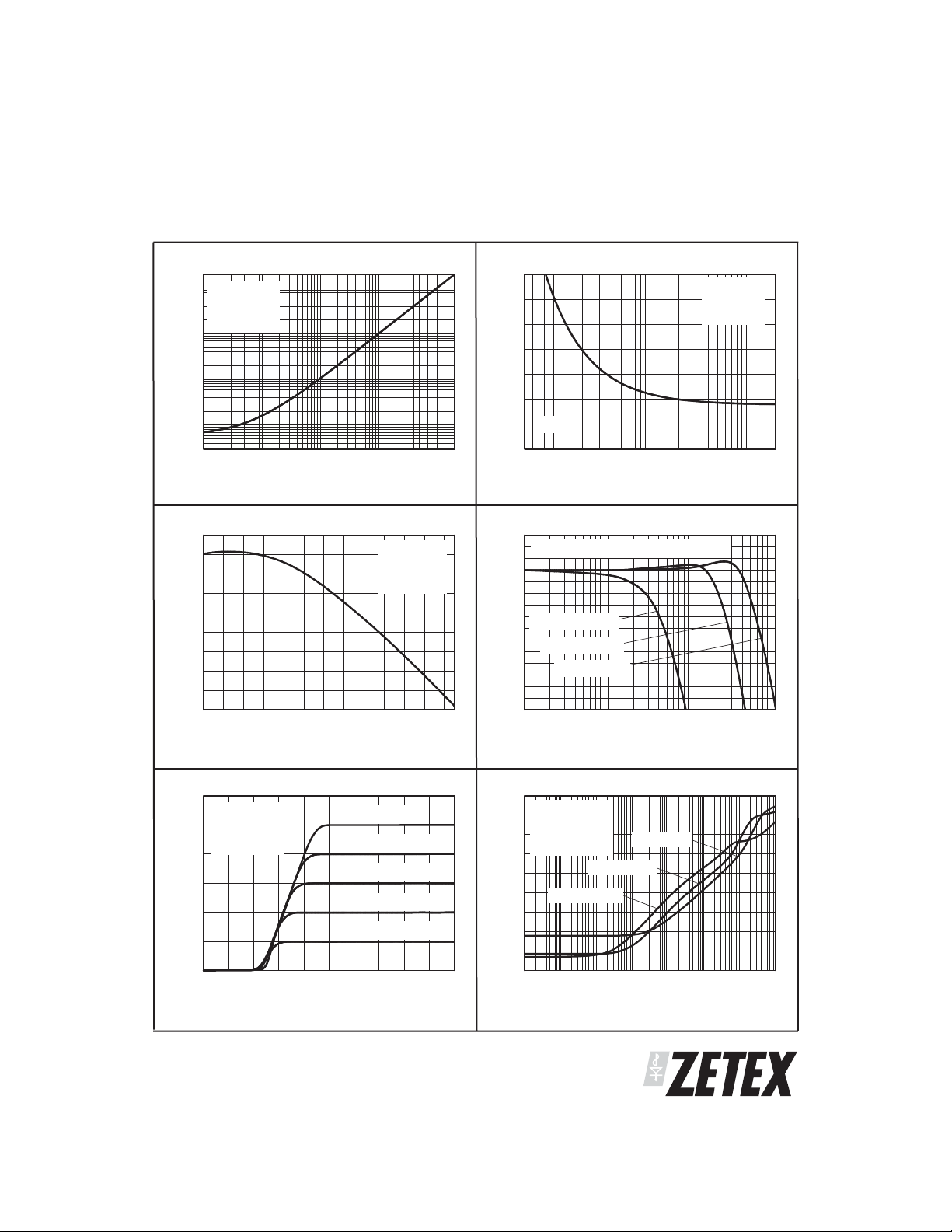
TYPICAL CHARACTERISTICS
ZXCT1009
10m
VIN=5V
Tamb = 25°C
R
=0
W
OUT
1m
100µ
- Output Current (A)
10µ
OUT
I
100µ 1m 10m 100m 1
V
SENSE
(V)
Typical Output v Sense Voltage
10.2
10.0
9.8
9.6
- Output Current (mA)
OUT
I
9.4
-40-20 0 20406080
Temperature (°C)
VIN=5V
V
SENSE
R
=0
OUT
Output Current v Temperature
=1V
W
Output Current Error (%)
5
4
3
2
1
0
-1
Typical
-2
10m 100m 1
V
SENSE
(V)
VIN=5V
Tamb = 25°C
R
OUT
Error v Sense Voltage
3
VIN=5V,Tamb=25°C,RFPIN=-20dBm
0
-3
DC V
-6
Gain (dB)
-9
-12
0.01 0.1 1 10
DC V
SENSE
SENSE
DC V
=0.01V
=0.1V
SENSE
=1V
Frequency (MHz)
Frequency Response
=0
W
12
VIN=5V
10
Tamb = 25°C
R
=0
W
OUT
8
6
4
- Output Current (mA)
2
OUT
I
0
012345
VIN- Supply Voltage (V)
Transfer Characteristic
ISSUE 9 - OCTOBER 2005
V
SENSE
V
SENSE
V
SENSE
V
SENSE
V
SENSE
=1V
=0.8V
=0.6V
=0.4V
=0.2V
0
VIN=5V
-10
Tamb = 25°C
-20
RF PIN= -20dBm
-30
-40
-50
V
=0.01V
SENSE
1 10 100 1k 10k 100k 1M 10M
Rejection (dB)
-60
-70
-80
-90
V
SENSE
V
SENSE
=0.1V
=1V
Frequency (Hz)
Common Mode Rejection
3
SEMICONDUCTORS
 Loading...