查询ZXCL1200H5供应商
ULTRA SMALL MICROPOWER SC70 2V 100mA REGULATOR
DESCRIPTION
The ZXCL200 is a very small 2 volt regulator designed
for use in low power and severely space limited
applications.
Supply current is minimised with a ground pin current
of only 40µA at full 100mA load. Logic control allows
the device to be shut down, consuming typically less
than 10nA. These features make it ideal for battery
powered applications where power economy is
critical.
The part has been designed with space sensitive
systems in mind. It is available in the ultra small SC70
package, which is half the size of other SOT23 based
regulator devices
ZXCL200
For applicationsrequiring improved performanceover
alternative devices,theZXCL200 is also offeredin the 5
pin SOT23 package with an industry standard pinout.
The devicefeatures thermal overload and over-current
protection.
The ZXCL200 is manufactured using CMOS
processing, however advanced design techniques
mean that output noise is improved even when
compared to other bipolar devices.
FEATURES
5-pin SC70 package for the ultimate in space
•
saving
5-pin SOT23 industry standard pinout
•
•
40µA ground pin current with full 100mA load
•
Typically less than 10nA ground pin current on
shutdown
•
2 volt output
•
Very low noise, without bypass capacitor
•
Thermal overload and over-current protection
•
-40 to +85°C operating temperature range
PACKAGE FOOTPRINT
Total Aea
2.1mm x 2mm
=4.2mm
Total Aea
2.8mm x 2.9mm
=8.12mm
2
2
APPLICATIONS
Cellular and Cordless phones
•
Palmtop and laptop computers
•
• PDA
•
Hand held instruments
•
Camera, Camcorder, Personal Stereo
•
PCMCIA cards
•
Portable and Battery-powered equipmenth
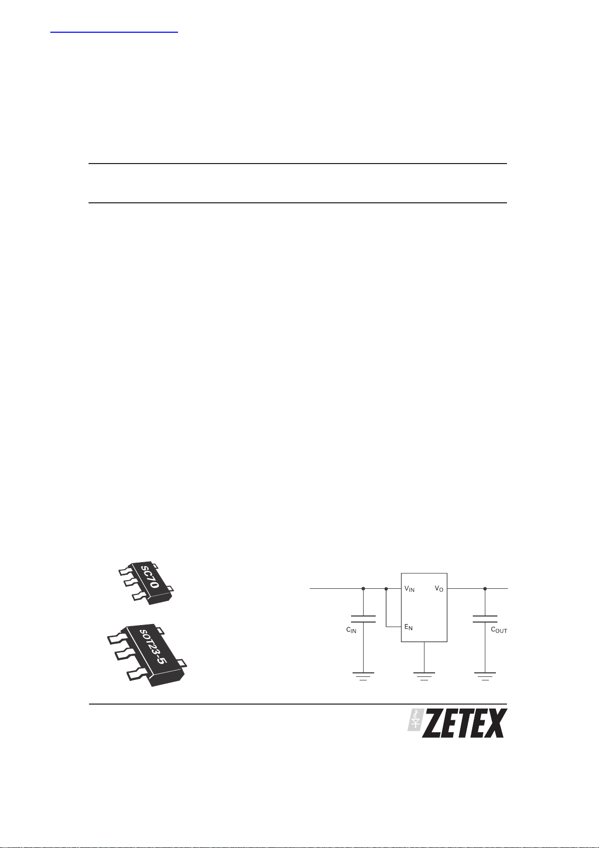
TYPICAL APPLICATION CIRCUIT
Battery Supply
ZXCL
Output Voltage
ISSUE 1 - SEPTEMBER 2001
1

ZXCL200
ABSOLUTE MAXIMUM RATINGS
Terminal Voltage with respect to GND
V
IN
E
N
V
O
Package Power Dissipation (T
SC70 300mW (Note 1)
SOT23-5 450mW (Note 1)
Stresses beyond those listed under “Absolute Maximum Ratings” may cause permanent damage to the
device. These are stress ratings only, and functional operation of the device at these or any other conditions
beyond those indicated in the operational sections of the specifications is not implied. Exposure to absolute
maximum conditions for extended periods may affect device reliability.
-0.3V to 7.0V
-0.3V to 10V
-0.3V to 5.5V
=25°C)
A
ELECTRICAL CHARACTERISTICS
V
= VO+ 0.5V, typical values at TA=25°C (Unless otherwise stated)
IN
SYMBOL PARAMETER CONDITIONS LIMITS UNITS
Output short circuit duration Infinite
Continuous Power Dissipation Internally limited
Operating Temperature Range -40⬚C to + 85⬚C
Storage Temperature Range -55⬚C to + 125⬚C
MIN TYP MAX
V
V
∆V
IN
O
O
Input Voltage TA=-40⬚C (note2) 5.5 V
/∆T
Output Voltage
(Note 3)
Output Voltage
=1mA
I
O
I
= 100mA
O
+0.5V < VIN<VINmax
V
O
1.96
1.94
22.04
-15 ppm/°C
Temperature
2.06
V
V
Coefficient
I
O(MAX)
I
OLIM
I
Q
⌬V
LNR
⌬V
LDR
E
N
V
ENH
V
ENL
Output Current 100
Over Current Limit
Ground pin current
No Load
= 100mA
I
O
105 750
25
40
50
100
Line Regulation VIN=(VO+0.5V) to 5.5V, IO=1mA 0.02 0.1 %/V
Load Regulation IO=1mA to 100mA 0.01 0.04 %/mA
Output Noise Voltage
Enable pin voltage for
normal operation
Enable pin voltage for
f=10Hz to 100kHz, C
T
= -40°C
A
=10µF,
O
2
2.2
00.8V
50
10 V
output shutdown
mA
mA
A
A
µV rms
Device testing is performed at TA=25⬚C. Device thermal performance is guaranteed by design.
Note 1: Maximum power dissipation is calculated assuming the device is mounted on a PCB measuring 2
inches square
Note 2: Output Voltage will start to rise when V
operation, V
Note 3: Nominal value of V
(min) > V
IN
(nom) + 0.5V.
OUT
is defined at VIN=VO+0.5V.
O
exceeds a value or approximately 1.3V. For normal
IN
ISSUE 1 - SEPTEMBER 2001
2

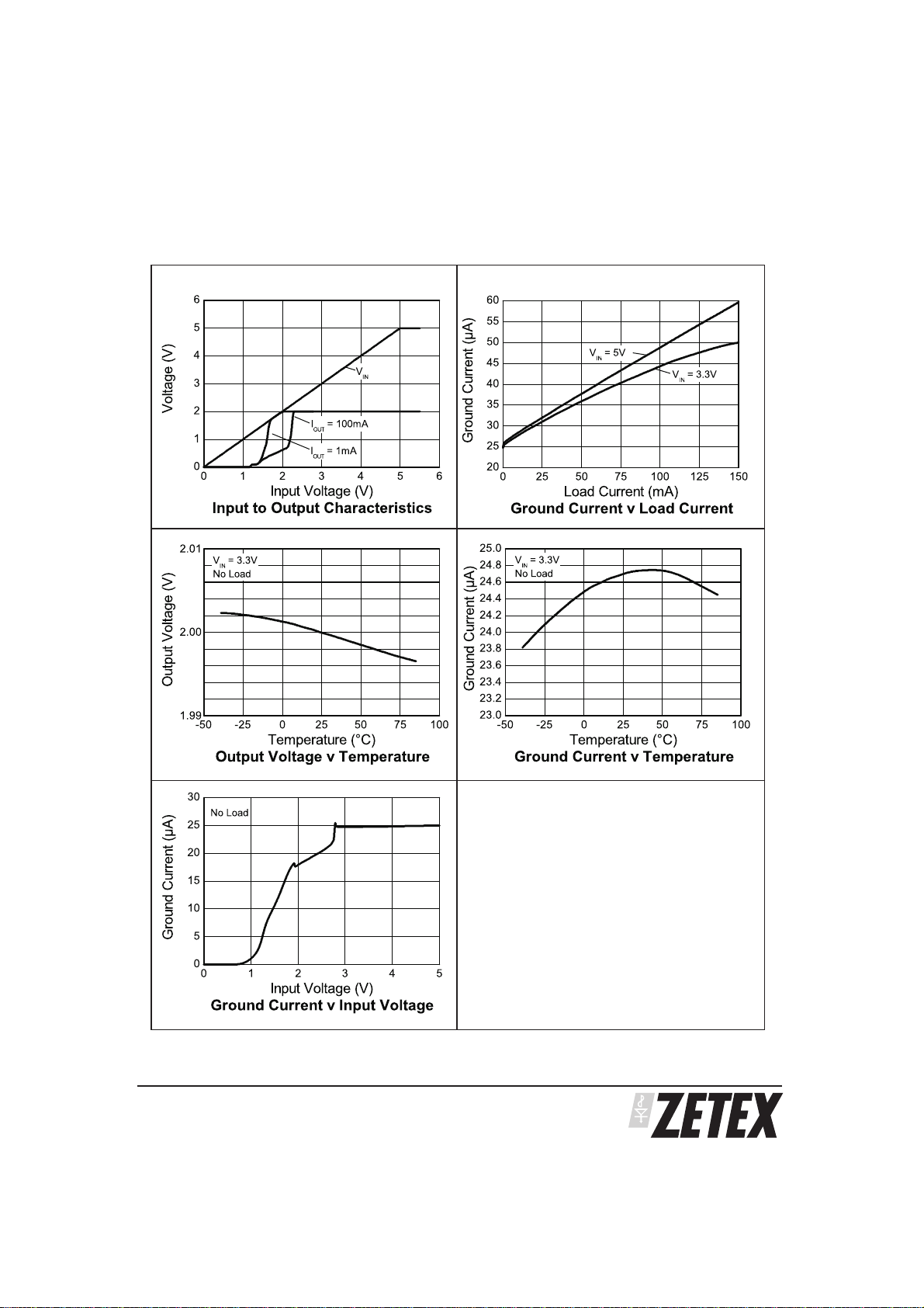
TYPICAL CHARACTERISTICS
ZXCL200
ISSUE 1 - SEPTEMBER 2001
3
 Loading...