

Zetex ZTX855 Datasheet
NPN SILICON PLANAR MEDIUM POWER
HIGH CURRENT TRANSISTOR
ISSUE 2 MARCH 94
FEATURES
* 150 Volt V
* 4 Amps continuous current
* Up to 10 Amps peak current
* Very low saturation voltage
*P
tot
ABSOLUTE MAXIMUM RATINGS.
PARAMETER SYMBOL VALUE UNIT
Collector-Base Voltage V
Collector-Emitter Voltage V
Emitter-Base Voltage V
Peak Pulse Current I
Continuous Collector Current I
Practical Power Dissipation* P
Power Dissipation at T
Operating and Storage Temperature Range T
*The power which can be dissipated assuming the device is mounted in a typical manner on a
P.C.B. with copper equal to 1 inch square minimum
ELECTRICAL CHARACTERISTICS (at T
PARAMETER SYMBOL MIN. TYP. MAX. UNIT CONDITIONS.
Collector-Base Breakdown
Voltage
Collector-Emitter Breakdown
Voltag
Collector-Emitter Breakdown
Voltage
Emitter-Base Breakdown
Voltage
Collector Cut-Off Current I
Collector Cut-Off Current I
Emitter Cut-Off Current I
Collector-Emitter Saturation
Voltage
Base-Emitter
Saturation Voltage
CEO
= 1.2 Watt
=25°C P
amb
V
(BR)CBO
V
(BR)CER
V
(BR)CEO
V
(BR)EBO
CBO
CER
R ≤1KΩ
EBO
V
CE(sat)
V
BE(sat)
CBO
CEO
EBO
CM
C
totp
tot
:Tstg -55 to +200 °C
j
= 25°C unless otherwise stated)
amb
250 375 V
250 375 V
150 180 V IC=10mA*
68 V
50
nA
1
µA
50
nA
1
µA
10 nA VEB=6V
20
35
60
210
60
100
260
mV
mV
mV
mV
40
960 1100 mV IC=4A, IB=400mA*
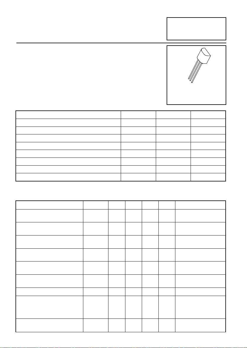
ZTX855
C
B
E
E-Line
TO92 Compatible
250 V
150 V
6V
10 A
4A
1.58 W
1.2 W
=100µA
I
C
µA, RB ≤1KΩ
IC=1
=100µA
I
E
=200V
V
CB
V
=200V, T
CB
V
=200V
CB
V
=200V, T
CB
I
=100mA, IB=5mA*
C
I
=500mA, IB=50mA*
C
=1A, IB=100mA*
I
C
I
=4A, IB=400mA*
C
amb
amb
=100°C
=100°C
2-300
ZTX855
ELECTRICAL CHARACTERISTICS (at T
amb
= 25°C)
PARAMETER SYMBOL MIN. TYP. MAX. UNIT CONDITIONS.
Base-Emitter
Turn-On Voltage
Static Forward
Current Transfer
V
h
BE(on)
FE
Ratio
Transition Frequency f
Output Capacitance C
Switching Times t
T
obo
on
t
off
*Measured under pulsed conditions. Pulse width=300
0.88 1 V IC=4A, VCE=5V*
100
100
35
200
200
55
10
300
I
I
I
I
90 MHz IC=100mA, VCE=10V
f=50MHz
22 pF VCB=20V, f=1MHz
66
2130
ns
ns
IC=1A, IB!=100mA
I
µs. Duty cycle ≤2%
=10mA, VCE=5V
C
=1A, VCE=5V*
C
=4A, VCE=5V*
C
=10A, VCE=5V*
C
=100mA, VCC=50V
B2
THERMAL CHARACTERISTICS
PARAMETER SYMBOL MAX. UNIT
Thermal Resistance: Junction to Ambient
Junction to Case
R
th(j-amb)
R
th(j-case)
150
50
°C/W
°C/W
)
s
tt
a
(W
tion
ipa
iss
D
ower
P
x
a
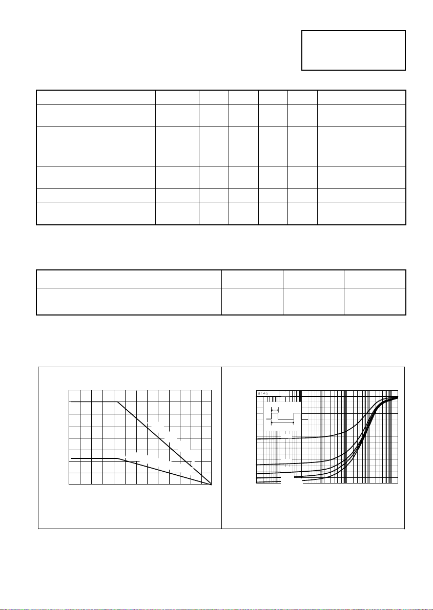
M
4.0
3.0
2.0
1.0
-40
-20 0 20
T -Temperature (°C)
Case te
mperatu
Ambien
t t
empe
rat
ure
40 60 80 100 120 200180160140
r
e
Derating curve
150
100
50
Thermal Resistance (°C/W)
0
Maximum transient thermal impedance
0.0001
D.C.
t
1
D=t
1/tP
t
P
D=0.6
D=0.2
D=0.1
D=0.05
Single Pulse
0.001
Pulse Width (seconds)
10 10010.10.01
3-301
 Loading...