Zetex ZSCT1555D8, ZSCT1555N8 Datasheet

PRECISION SINGLE CELL TIMER
ISSUE 2 - MAY 1998
DEVICE DESCRIPTION
These devices are precision timing circuits for
generation of accurate time delays or
oscillation. Advanced circuit design means that
these devices can operate from a single battery
cell with the minimum of quiescent current.
In monostable mode time delays are
controlled by a single resistor and capacitor
network. In astable mode the frequency and
duty cycle can be accurately and
independently controlled with two external
resistors and one capacitor.
The threshold and trigger levels are normally
set as a proportion of V
These levels can be programmed by the use
of the control input pin.
When the trigger input reduces to a value
below the trigger level, the flip-flop is set and
the output goes high. With the trigger input
above the trigger level and the threshold input
above the threshold level, the flip-flop is reset
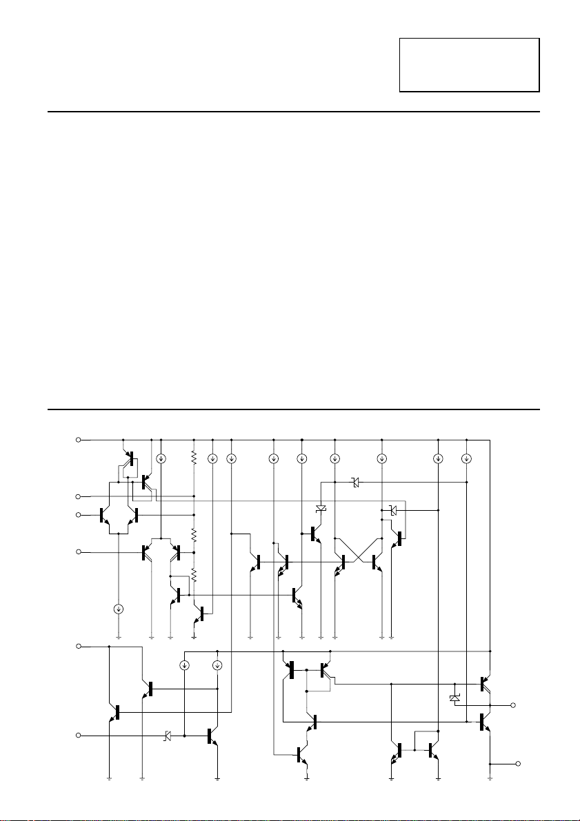
SCHEMATIC DIAGRAM
8
VCC
by internal resistors.
CC
ZSCT1555
and the output goes low. The reset pin has
priority over all the other inputs and is used
to start new timing cycles. A low on the reset
input causes the flip-flop to reset forcing the
output low. Whenever the output is forced
low then the internal discharge transistor is
turned on.
FEATURES
0.9V supply operating voltage guaranteed
•
Pin connections comparable with 555
•
series timers
Very low quiescent current 74 µA
•
SO8 and DIL8 packages
•
Operating temperature range
•
compatible with battery technologies
APPLICATIONS
Portable and battery powered
•
equipment
Low voltage and low power systems
•
CONTROL
5
6
THRESH
2
TRIGGER
7
DISCHARGE
4
RESET
4-311
3
OUTPUT
GND
1

ZSCT1555
ABSOLUTE MAXIMUM RATINGS
Supply Voltage 9V
Input Voltages 9V
(Cont, Reset, Thres, Trig)
Output Current 100mA
Operating Temperature -20 to 100°C
Storage Temperature -55 to 150°C
ELECTRICAL CHARACTERISTICS
TEST CONDITIONS (Unless otherwise stated):T
SYMBOL PARAMETER CONDITIONS
V
CC
I
CC
V
TH
I
TH
V
TR
I
TR
t
PD
V
RS
I
RS
I
DS
V
DS
V
CT
V
OL
V
OH
Supply Voltage 0.9 6 V
Supply Current no load
Threshold Voltage
Threshold Current (Note 1) 0 20 100 nA
Trigger Voltage
Trigger Current 0 -35 -100 nA
Trigger Propagation delay Delay from trigger
Reset Voltage 0.1 0.2 0.4 V
Reset Current Reset @ 0V 0 -5 -10
Discharge switch Off-state
current
Discharge switch On-state
voltage
Control Voltage (Open Circuit)
Output Voltage (Low) IOL=10mA
Output Voltage (High)
Power Dissipation (T
DIL8 625mW
SO8 625mW
Recommended Operating Conditions
Supply Voltage 0.9V(min) 6V(max)
Input Voltages 6V(max)
(Cont, Reset, Thres, Trig)
Output Current Sink 100mA(max)
Source 150µA(max)
V
= 5V, no load
CC
V
= 5V
CC
V
= 5V
CC
to output
IDS= 0.2mA
= 5V, IDS= 0.3mA00
V
CC
V
= 5V
CC
I
=50mA
OL
V
=5V, IOL=10mA
CC
V
=5V, IOL=100mA
CC
= 100µA
I
OH
V
= 5V, IOH= 150µA
CC
= 25°C,VCC= 1.5V
amb
MIN. TYP. MAX.
1.195
3.9
0.2
0.57
0 10 100 nA
1.195
3.9
0
0
0
0
1
4.5
=25°C)
amb
LIMITS
74
150
1.2241.245
0.25
0.62
2
180
240
1.2241.245
0.15
0.45
0.13
0.65
1.1
4.6
120
200
4.1
0.3
0.67
225
350
4.1
0.3
0.65
0.3
1
1.55V
UNITS
mA
V
V
µs
µA
mV
V
V
4-312

ZSCT1555
ELECTRICAL CHARACTERISTICS (Continued)
TEST CONDITIONS (Unless otherwise stated):T
SYMBOL PARAMETER CONDITIONS
t
R
t
F
∆t
IA
∆t
V
∆t
T
∆tIA(a)
∆t
V
∆t
T
f
A
Note 1: This will influence the maximum values of RA and RB (RA
Note 2: Is defined as the difference between the measured value and the average value of a
random sample taken on a batch basis
Output pulse rise time CL= 10pF
Output pulse fall time CL= 10pF
Timing error, Monostable
Initial accuracy (Note 2)
(m)
Drift with supply voltage
(m)
Drift with temperature
(m)
Timing error, Astable
Initial accuracy (Note 2)
Drift with supply voltage
(a)
Drift with temperature
(a)
Astable maximum frequency
V
=5V, CL=10pF
CC
V
=5V, CL=10pF
CC
RA= 10 to 50 kΩ
RB= 10 to 50 kΩ
= 68nF
C
T
RA= 10 to 50 kΩ
RB= 10 to 50 kΩ
= 68nF
C
T
RA=20 kΩ
RB= 10 kΩ
=47pF
C
T
=25°C,VCC=1.5V
amb
MIN. TYP. MAX.
MAX
LIMITS
1.6
1.2
240
24
1.6
0.262
100
4.8
0.662
150
=10MΩ,RB
330 kHz
=1.5MΩ)
MAX
UNITS
µs
ns
%
%/V
ppm/°C
%
%/V
ppm/°C
4-313
 Loading...