

6.2V LOW POWER
PRECISION REFERENCE SOURCE
ISSUE 1 - OCTOBER 1995
DEVICE DESCRIPTION
The ZRT062 is a monolithic integrated circuit
providing a precise stable reference voltage
of 6.17V at 500µA.
The circuit features a knee current of 150µA
and operation over a wide range of
temperatures and currents.
The ZRT062 is available in a 3-pin metal can
package for through hole applications as
well as SOT223 and SO8 packages for
surface mount applications. Each package
option offers a trim facility whereby the
output voltage can be adjusted as shown in
Fig.1. This facility is used when
compensating for system errors or setting
the reference output to a particular value.
When the trim facility is not used, the pin
should be left open circuit.
SCHEMATIC DIAGRAM
ZRT062
FEATURES
Trimmable output
•
Excellent temperature stability
•
Low output noise figure
•
Available in two temperature ranges
•
1 and 2% initial voltage tolerance
•
versions available
No external stabilising capacitor
•
required in most cases
Low slope resistance
•
TO18 package
•
SOT223 and SO8 small outline packages
•
R
CC
V
R=VCC-V
G
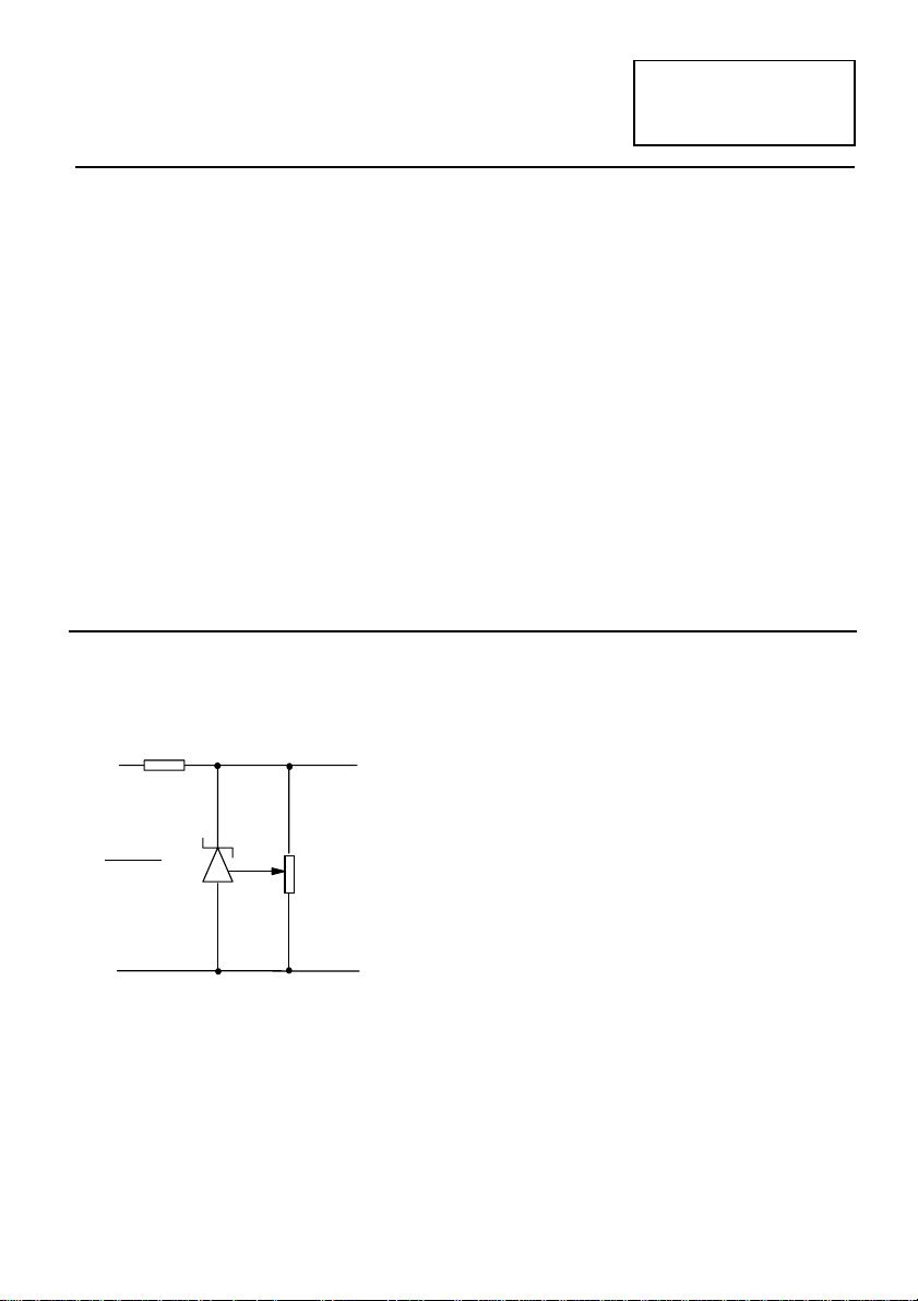
Figure 1:
This circuit will allow the reference to be
trimmed over a wide range. The device is
specified over a 65% trim range.
R
R
I
nd
RT=100k
(Optional trim facility)
R
V
nd
G
4-291
ZRT062
ABSOLUTE MAXIMUM RATING
Reverse Current 50mA ø
Operating Temperature
A grade -55°C to 125°C
C grade 0°C to 70°C
Storage Temperature
TO18 -55 °C to 175 °C
Power Dissipation (T
TO18 300mW
SO8 625mW
SOT223 2W
ø Above 25°C this figure should be linearly
derated to 10mA at 125°C
SO8, SOT223 -55 °C to 125 °C
TEMPERATURE DEPENDENT ELECTRICAL CHARACTERISTICS
SYMBOL PARAMETER
DV
R
Output voltage
change over relevant
temperature range
(See note (a))
T
CVR
Output voltage
temperature
coefficient
(See note (b))
INITIAL
VOLTAGE
TOLERANCE
%
1 & 2 15.0 40.0 6.5 22.0 mV
1 & 2 15.0 40.0 15.0 50.0 ppm/°C
GRADE A
-55°C TO 125°C
GRADE C
0°C TO 70°C
TYP MAX TYP MAX
ELECTRICAL CHARACTERISTICS
( at T
SYMBOL PARAMETER
V
DV
T
I
R
t
on
t
off
e
R
=25°C and Trim pin o/c unless otherwise stated)
amb
MIN. TYP.
R
Output voltage
1% tolerance (A1,C1)
2% tolerance (C2)
Output voltage adjustment
TRIM
6.11
6.17
6.05
6.17
65%
range
CDVTRIM
Change in TCVR with output
5.0 ppm/°C/%
adjustment
Operating current range 0.15 50 mA See note (c)
np-p
Turn-on time
Turn-off time
Output voltage noise (over the
250
0.3
50
range 0.1 to 10Hz)
S
Slope resistance 1.4 3.0
MAX. UNITS
6.23
V
6.29
µsR
µV
Ω
amb
=25°C)
UNITS
COMMENTS
I
=500µA
R
=100kΩ
R
T
=1kΩ
L
Peak to peak
measurement
IR =
0.5mA to 5mA
See note (d)
4-292
TYPICAL CHARACTERISTICS
ZRT062
NOTES
(a) Output change with temperature (VR)
The absolute maximum difference between
the maximum output voltage and the
minimum output voltage over the specified
temperature range
D
(b) Output temperature coefficient (TCVR)
The ratio of the output change with
temperature to the specified temperature
range expressed in ppm/°C
TcV
R
∆T= Full temperature range
=
VR = V
V
x
10
∆
R
V
x ∆
R
- V
max
min
6
ppm
⁄
°
C
T
(c) Operating current (I
)
R
Maximum operating current must be
derated as indicated in maximum ratings.
(d) Slope resistance (R
)
S
The slope resistance is defined as :
change
in
V
R
=
S
specifiedcurrentrange
∆
I = 5 - 0.5 = 4.5mA (typically)
R
(e) Line regulation
The ratio of change in output voltage to the
change in input voltage producing it.
R
x 100
S
V
x
R
R
source
% ⁄
V
4-293

ZRT062
CONNECTION DIAGRAMS
SOT223 Package Suffix – G
Top View
Pin 4 floating or connected to pin 2
TO18 Package Suffix – None
Bottom View –
Case is internally connected to pin 3
SO8 Package Suffix – N8
Top View
ORDERING INFORMATION
Part No Tol% Operating
Temp.(°C)
ZRT062C2 2 0 to 70 TO18 ZRT062C2
ZRT062C1 1 0 to 70 TO18 ZRT062C1
ZRT062A1 1 -55 to 125 TO18 ZRT062A1
ZRT062GC2 2 0 to 70 SOT223 ZRT062C2
ZRT062GC1 1 0 to 70 SOT223 ZRT062C1
ZRT062GA1 1 -55 to 125 SOT223 ZRT062A1
ZRT062N8C2 2 0 to 70 SO8 ZRT062C2
ZRT062N8C1 1 0 to 70 SO8 ZRT062C1
ZRT062N8A1 1 -55 to 125 SO8 ZRT062A1
Package Partmark
4-294
 Loading...