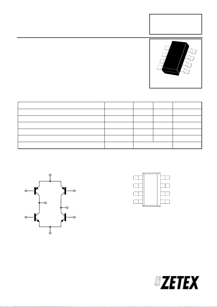
Zetex ZHB6718 Datasheet

SM-8 BIPOLAR TRANSISTOR H-BRIDGE
SM-8
(8 LEAD SOT223)
PRELIMINARY DATA SHEET ISSUE B - JULY 1997
FEATURES
* Compact package
* Low on state losses
* Low drive requirements
* Operates up to 20V supply
* 2.5 Amp continuous rating
PARTMARKING DETAIL ZHB6718
ABSOLUTE MAXIMUM RATINGS.
PARAMETER SYMBOL NPNs PNPs UNIT
Collector-Base Voltage V
Collector-Emitter Voltage V
Emitter-Base Voltage V
Peak Pulse Current I
Continuous Collector Current I
Operating and Storage Temperature Range T
CBO
CEO
EBO
CM
C
j:Tstg
20 -20 V
20 -20 V
2.5 -2.5 A
ZHB6718
5-5 V
6-6 A
-55 to +150 °C
SCHEMATIC DIAGRAM
E1, E4
B1
B2
Q2 Q3
Q4Q1
C1, C2
E2, E3
C3, C4
B4
B3
CONNECTION DIAGRAM
C1,C
E1,E
C3,C
B
5
2
6
4
7
4
4
8
4
B
3
B
2
E2,E
1
B
1
2
3
3

ZHB6718
THERMAL CHARACTERISTICS
PARAMETER SYMBOL VALUE UNIT
Total Power Dissipation at T
Any single transistor on
= 25°C*
amb
Q1 and Q3 on or Q2 and Q4 on equally
Derate above 25°C*
Any single transistor on
Q1 and Q3 on or Q2 and Q4 on equally
Thermal Resistance - Junction to Ambient*
Any single transistor on
Q1 and Q3 on or Q2 and Q4 on equally
P
tot
R
th(j-amb)
1.25
2
10
16
100
62.5
mW/ °C
mW/ °C
°C/ W
°C/ W
W
W
100
D=t1
t1
80
60
40
20
0
100us
tP
tP
D=1
D=0.5
D=0.2
D=0.1
D=0.05
Single Pulse
1ms 10ms 100ms 1s 10s 100s
Pulse Width
Transient Thermal Resistance
Single Transistor "On"
2.0
1.5
1.0
0.5
0
020
40 60 80 100 140120 160
T - Temperature (°C)
Derating curve
* The power which can be dissipated assuming the device is mounted in a typical manner on a PCB
with copper equal to 2 inches square.
Two devices on is the standard operating condition for the bridge. Eg opposing NPN/PNP pairs
turned on.
60
50
40
30
20
10
0
t1
1ms100us
tP
D=t1
tP
10ms
Pulse Width
1s100ms
Transient Thermal Resistance
Q1 and Q3 or Q2 and Q4 "On"
10
1
0.1
0.1
Minimum Copper
Pcb Area (inches squared)
Full Copper
110
Pd v PCB Area Comparison
D=1
D=0.5
D=0.2
D=0.1
D=0.05
Single Pulse
10s
Two devices on
Single device on
Two devices on
Single device on
100s

ZHB6718
NPN TRANSISTORS
ELECTRICAL CHARACTERISTICS (at T
PARAMETER SYMBOL MIN. TYP. MAX. UNIT CONDITIONS.
Collector-Base
Breakdown Voltage
Collector-Emitter
Breakdown Voltage
Emitter-Base Breakdown
Voltage
Collector Cut-Off Current I
Emitter Cut-Off Current I
Collector Emitter Cut-Off
Current
Collector-Emitter
Saturation Voltage
Base-Emitter
Saturation Voltage
Base-Emitter Turn-On
Voltage
Static Forward Current
Transfer
Ratio
Transition
Frequency
Output Capacitance C
Turn-On Time t
Turn-Off Time t
*Measured under pulsed conditions. Pulse width=300µs. Duty cycle ≤ 2%.
V
(BR)CBO
V
(BR)CEO
V
(BR)EBO
CBO
EBO
I
CES
V
CE(sat)
V
BE(sat)
V
BE(on)
h
FE
f
T
obo
(on)
(off)
20 100 V
20 27 V IC=10mA*
5 8.3 V
200
300
200
100 140 MHz IC=50mA, VCE=10V
= 25°C ).
amb
=100µA
I
C
=100µA
I
E
100 nA VCB=16V
100 nA VEB=4V
8
70
130
100 nA V
15
mV
150
mV
200
mV
=16V
CES
IC=0.1A, IB=10mA*
I
=1A, IB=10mA*
C
I
=2.5A, IB=50mA*
C
0.89 1.0 V IC=2.5A, IB=50mA*
0.79 V IC=2.5A, VCE=2V*
400
450
360
180
IC=10mA, VCE=2V*
=100mA, VCE=2V*
I
C
=2A, VCE=2V*
I
C
I
=6A, VCE=2V*
C
f=100MHz
23 30 pF VCB=10V, f=1MHz
170 ns VCC=10V, IC=1A
I
=-IB2=10mA
400 ns
B1
 Loading...