Zetex ZDT751 Datasheet

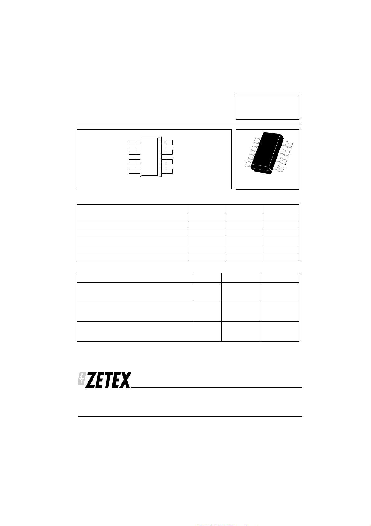
SM-8 DUAL PNP MEDIUM POWER
TRANSISTORS
ISSUE 1 - AUGUST 1997
ZDT751
C
1
C
1
C
2
C
2
B
1
E
1
B
2
E
2
SM-8
PARTMARKING DETAIL – T751
(8 LEAD SOT223)
ABSOLUTE MAXIMUM RATINGS.
PARAMETER SYMBOL VALUE UNIT
Collector-Base Voltage V
Collector-Emitter Voltage V
Emitter-Base Voltage V
Peak Pulse Current I
Continuous Collector Current I
Operating and Storage Temperature Range T
CBO
CEO
EBO
CM
C
j:Tstg
-80 V
-60 V
-5 V
-6 A
-2 A
-55 to +150 °C
THERMAL CHARACTERISTICS
PARAMETER SYMBOL VALUE UNIT
Total Power Dissipation at T
Any single die “on”
Both die “on” equally
Derate above 25°C*
Any single die “on”
Both die “on” equally
Thermal Resistance - Junction to Ambient*
Any single die “on”
Both die “on” equally
* The power which can be dissipated assuming the device is mounted in a typical manner
on a PCB with copper equal to 2 inches square.
= 25°C*
amb
P
tot
2.25
2.75
18
22
55.6
45.5
W
W
mW/ °C
mW/ °C
°C/ W
°C/ W
Zetex plc.
Fields New Road, Chadderton, Oldham, OL9-8NP, United Kingdom.
Telephone: (44)161-627 5105 (Sales), (44)161-627 4963 (General Enquiries)
Fax: (44)161-627 5467
Zetex GmbH Zetex Inc. Zetex (Asia) Ltd. These are supported by
Streitfeldstraße 19 47 Mall Drive, Unit 4 3510 Metroplaza, Tower 2 agents and distributors in
D-81673 München Commack NY 11725 Hing Fong Road, major countries world-wide
Germany USA Kwai Fong, Hong Kong
Telefon: (49) 89 45 49 49 0 Telephone: (516) 543-7100 Telephone:(852) 26100 611 Internet:
Fax: (49) 89 45 49 49 49 Fax: (516) 864-7630 Fax: (852) 24250 494 http://www.zetex.com
This publication is issued to provide outline information only which (unless a greed by the Company in writing) may n ot be used, applied
or reproduced for any purpose or form part of any order or cont rac t or be regarded as a repres entat ion rel ati ng to the product s or
services concerned. The Company reserves the right to alt er wit h out noti ce the s pecif icati on, design, price or conditions of supply of any
product or service.
Zetex plc 1997

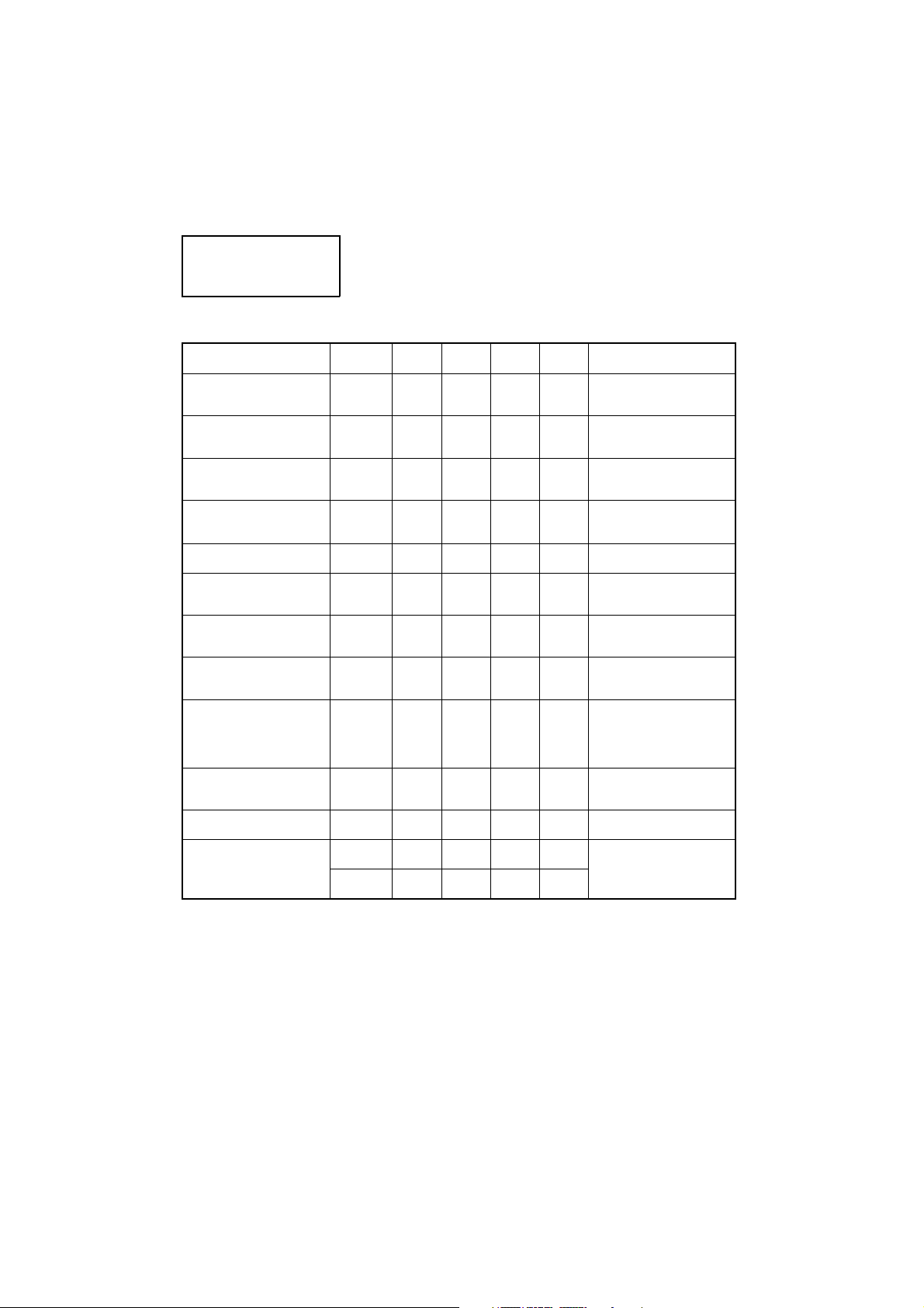
ZDT751
ELECTRICAL CHARACTERISTICS (at T
= 25°C unless otherwise stated).
amb
PARAMETER SYMBOL MIN. TYP. MAX. UNIT CONDITIONS.
Collector-Base
Breakdown Voltage
Collector-Emitter
Breakdown Voltage
Emitter-Base
Breakdown Voltage
Collector Cutoff
Current
Emitter Cutoff Current I
Collector-Emitter
Saturation Voltage
Base-Emitter
Saturation Voltage
Base-Emitter
Turn-On Voltage
Static Forward Current
Transfer Ratio
Transition Frequency f
V
(BR)CBO
V
(BR)CEO
V
(BR)EBO
I
CBO
EBO
V
CE(sat)
V
BE(sat)
V
BE(on)
h
FE
T
-80 V
I
=-100µA, IE=0
C
-60 V IC=-10mA, IB=0*
-5 V
-0.1
-10
-0.1
-0.15
-0.28
-0.3
-0.5VV
µA
µA
µA
I
=-100µA, IC=0
E
VCB=-60V
V
=-60V,T
CB
VEB=-4V, IE=0
IC=1A, IB=-100mA*
I
=2A, IB=-200mA*
C
-0.9 -1.25 V IC=1A, IB=-100mA*
-0.8 -1 V IC=-1A, VCE=-2V*
70
100
80
40
200
200
170
80
300
I
=-50mA, VCE=-2V*
C
I
=-500mA, VCE=-2V*
C
I
=-1A, VCE=-2V*
C
I
=-2A, VCE=-2V*
C
100 140 MHz IC=-100mA, VCE=-5V
f=100MHz
amb
=100°C
Output Capacitance C
Switching Times t
obo
on
t
off
40 ns IC=-500mA, VCC=-10V
450 ns
30 pF VCB=-10V f=1MHz
*Measured under pulsed conditions. Pulse width=300µs. Duty cycle ≤ 2%
I
B1=IB2
=-50mA
 Loading...