Zetex ZDS1009 Datasheet

SM-8 COMPLEMENTARY CURRENT MIRROR
ZDS1009
DESCRIPTION
The ZDS1009 current mirror has been developed
specifically for high side, current sense plus level
translation applications and as such will find a broad
applications base including battery charge
management, DC motor control and over current
monitoring functions. It is of particular interest for
current sense applications for feedback purposes in fast
battery chargers for Li-Ion cell based systems.
FEATURES
Excellent Temperature Tracking Characteristics
•
Compact Cost Effective Solution
•
Simplifies Circuit Implementation
•
Broad application base from
•
Single Cell Li-ion High Side Current sense chargers to
Multi-cell Lead-Acid systems
• Only 4 Connections required
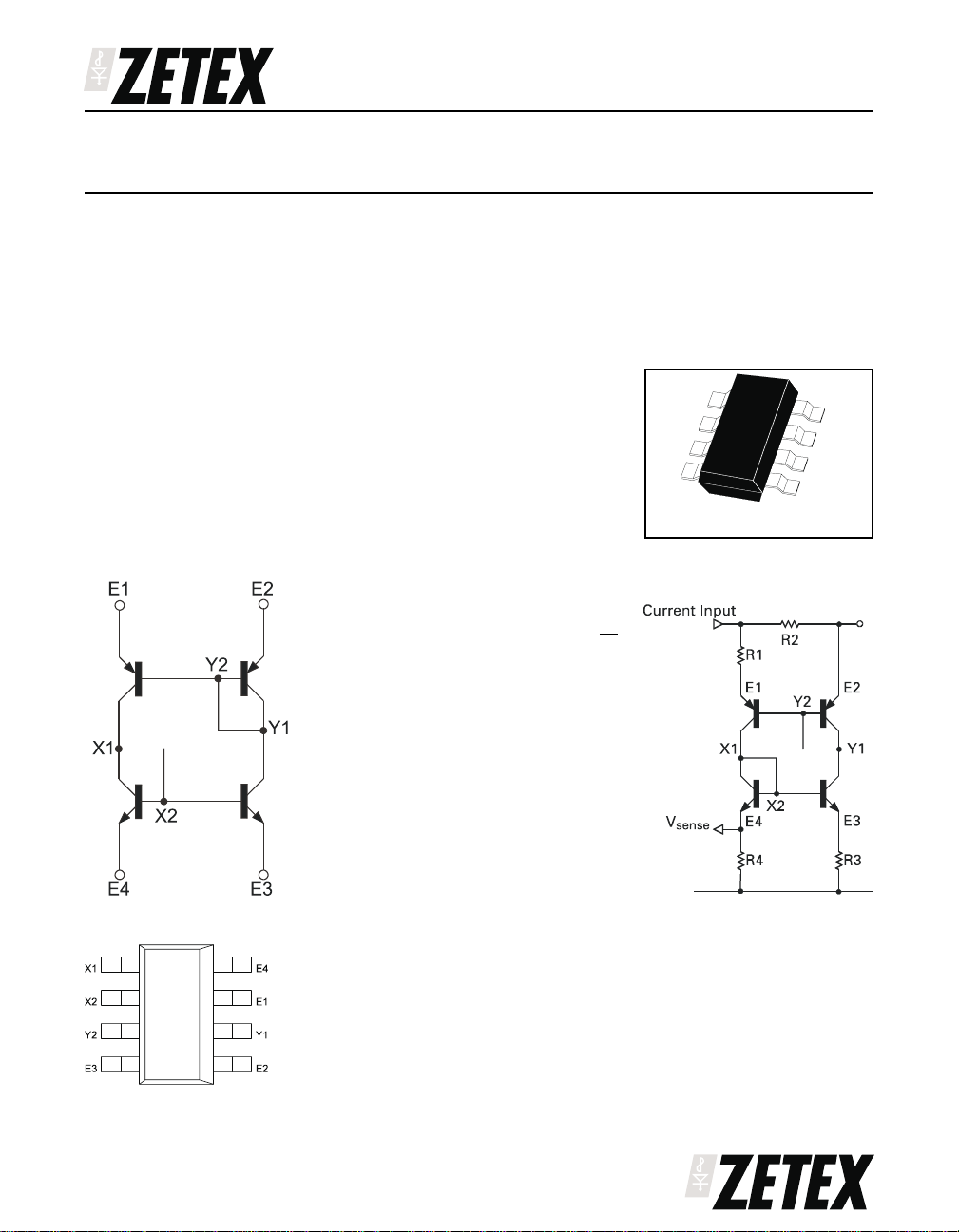
SCHEMATIC DIAGRAM
Thedevicefunctionsbysensing the voltagedeveloped
across an external (user defined) high side current
sense resistor, and by an arrangement of current
mirrors refer this sensed voltage, with or without
multiplication, to a low side referenced signal. This
signal can then be used, for example, to close the
control loop to a controller IC, for a DC-DC converter
providing charge to a battery.
SM-8
(8 LEAD SOT223)
TYPICAL APPLICATION CIRCUIT
R
VIR
sense 2
For balance R3=R4
R2=100mΩ
R1=R3=R4=100Ω
4
=
R
1
eg
CONNECTION DIAGRAM
ISSUE 2 - JANUARY 2000
sensitivity = 100mV/A
V
sense
1

ZDS1009
ABSOLUTE MAXIMUM RATINGS.
PARAMETER SYMBOL VALUE UNIT
Maximum Operating Voltage V
Maximum Voltage (E1-E2,E3-E4) V
Peak Pulse Current I
Continuous Current (E1-E4,E2-E3) I
Total Power Dissipation at T
= 25°C* P
amb
Operating and Storage Temperature Range T
* The power which can be dissipated assuming the device is mounted in a typical manner on a PCB with copper
equal to 2 inches square.
ELECTRICAL CHARACTERISTICS (at T
=25°C)
amb
y1-x1
E-E’
M
C
tot
j:Tstg
Parameter Symbol Min Max Unit Conditions
Breakdown Voltage BV
Breakdown Voltage BV
Breakdown Voltage BV
Breakdown Voltage BV
Breakdown Voltage BV
Breakdown Voltage BV
Breakdown Voltage BV
Leakage I
Leakage I
Leakage I
Leakage I
Leakage I
Leakage I
Leakage I
Y1
X1
Y1
E1
E2
E3
E4
Input Voltage V
Input Voltage V
Input Voltage V
Input Voltage V
Transfer
V
Characteristic
Transfer
V
Characteristic
Output Zero-Offset
V
Voltage
Y1-X1
X1-E1
Y1-E3
E1-Y1
E2-Y1
E3-X1
E4-X1
Y1-E2
Y1-E3
X1-E1
X1-E4
OUT
OUT
OFFSET
120 V
-30 V IX1=-10mA
30 V IY1=10mA
-12 V
-6 V
12 V
6VI
50 nA V
-10
10
µA
µA
-100 nA V
-100 nA V
100 nA V
100 nA V
-1.45 -1.65 V IY1=-1A
1.45 1.75 V IY1=1A,VX1=V
-1.45 -1.75 V IX1=-1A,VX1=V
1.45 1.65 V IX1=1A
0.99 1.01 V See Fig 1.VCC=5V
1 mV See Fig 1.VCC=5V
4mV
120 V
10 V
4A
1A
2W
-55 to +150 °C
I
=100µA
Y1
I
=-100µA
E1
I
=-100µA
E2
I
=100µA
E3
=100uA
E4
=100V
Y1-X1
V
=-30V, Vy1=V
X1-E1
V
=30V,VX1=V
Y1-E3
=-8V
E1-Y1
=-4V
E2-Y1
=8V
E3-X1
=4V
E4-X1
R1=R3=R4=100Ω,V
R1=R3=R4=100Ω,V
See Fig 2.V
R1=R3=R4=100Ω
E3
Y1
Y1
=5V,R2<1Ω
CC
E1
IN
IN
=1V
=5mV
ISSUE 2 - JANUARY 2000
2
 Loading...