

Page 1
TT-27
;T!1f1'H
Technical
Z-39
VIDEO
TERMINAL
~::tems
585-169
Training
DISPLAY
Page 2

Contents
Chapter
Introduction
THE
LIST
LIST
LIST
SPECIFICATIONS
1:
Description
Z-39
OF
TOO
OF
TEST
OF
SUPPLIES
SERVICE
DISPLAy
CURSOR
KEyBOARD
EDITING
TERMINAL
PRIliTER
ENYIRONMENT
POWER
DIMENSIONS
Installation
Voltale
leyboard
Video
Conneotions
Interfacing
DTE
SELF-CHECK TESTS
POWER-ON
•••••••••••••••••••••
••••••••••••••••••••••••••••••••••••••••••••••••••
Keyboard
leyboard
Display
and
INDICATOB
and
Specifications
•••••••••••••••••••••••••••
MANUAL
LS
•••••••••••••••••••••••••••••••••••••••••••
EQUIPMEIT
•••••••••••••••••••••••
•••••••••••••••••••••••••
••••••••••••••••
•••••••••••••••••
••••••••••••••••••••
· ................. .
· ................. .
· ................. .
· ................. .
•
••••••••••••••••••
••••••••••••••••••••••••••••••••••••••••••••••••
a.a
••••••••••••••••••••••••••
•••••••••••••••••••••••••••••••••••••••••••••••
AND
ERASIliG
COMMUNICATIONS
COMMUNICATIO.S
••••••••••••••••••••••••••••••••••••••••••••
•••••••••••••••••••••••••••••••••••••••••••••
••••••••••••••••••••••••••••••••••••••••••••••
Selection
•••••••••••••••••••••••••••••••••••••••••••••••
Indicators
Tilt
Un1t
•••••••••••••••••••••••••••••••••••••••••••
••••••••••••••••••••••••••••••••••••••••••••••
DCE
Devices
•••••••••••••••••••••••••••••••••••••••••
•••••••••••••••••••••••••••••••••••••••
FUNCTIONS
•••••••••••••••••••••
•••••••••••••••••••••••••••••••••
•••••••••••••••••••••••••••••••••••••
•••••••••••••••••••••••••••••••••
Adjustment
•••••••••••••••••••••••••••••••••••••
•••••••••••••••••••••••••••••••••••
••••••••
•••••••••••••••••••••••••••
..................
. . . . . . . . . . .
1-10
1-10
1~11
1-14
1-14
1-15
1-15
1-1
1-1
1-2
1-2
1-3
1-3
1-4
1-4
1-4
1-5
1-5
1-5
1-6
1-6
1-6
1-6
1-7
1-7
1-9
1-7
Chapter
Theory
DETAILED
2:
General
of
Operation
Vertical
Video
Horizontal
Horizontal
I:EYBOARD
TERMINAL
VIDEO
POWER
Amplifier
CIRCUIT DESCRIPTION
Pover-Up
Serial
CPU
and
"e.o~,
CLOCK
CHARACTER
DEFLECTION/DRIYER CIRCUIT
Vertical
Horizontal
Horizontal
Video
su~PLr
Infor.ation
•••••••••••••••••••••••••••••••••••••••
Oscillator
Oscillator
Scan
ASSEMBLY
LOGIC
and
Ports
Control
Map
••••••••••••••••••••••••••••••••••••••••••
CIRCUIT
GENERATION......................
Circuits
Clrcuits
Scan
Amplifier
••••••••••••••••••••••••••••••••••••
••••••••••••••••••••••••••••••••••••••••
and
Pover
••••••••••••••••••••••••••••••••••••••
BOARD
••••••••••••••••••••••••••••••••••••••••
•••••••••••••••••••••••••••••••••••
Beset
Circuitry
••••••••••••••••••••••••••••••••••••••
••••••••••••••••••••••••••••••••••
and
•••••••••••••••••
••••••••••••••••••••••••••••••
••••••••••••••••••••••••••••••••••
Supplies
••••••••••••••••••••••••••••••
Circuit......
•••••••••••••••••••••••••••
••••••••••••••••••••••••••••••••
Pover
Supplies
•••••••••••••••••••••
BOARDS
. . . . . . . . . . . . . . .
••••••••••••••••••••••••••••••••••••••••••
•
••••••••••••••••
••••••••••••••••
•••••••••••••••••
•
••••
••••
2-1
2-1
2-2
2-2
2-2
2-2
2-3
2-3
2-4
2-4
2-5
2-7
2-9
2-11
2-12
2-15
2-15
2-15
2-16
2-17
2-17
i
Page 3

Cbapter
Introduction
KEyBOARD
ALPHABETIC
CONTROL
SPECIAL PURPOSE KEyS
lEY
Setup
Entering
Menu
3:
Operation
••••••••••••••••••••••••••••••••••••••••
••••••••••••••••••••••••••••••••••••••••••••••
•••••••••••••••••••••••
IEyS
••••••••••••••••••••••••••••••••••••••••
NOHALPHABETIC KEyS
FORMAT
PAD
IEYS
Mode
••••••••••••••••••••••••••••••••••••••••••••••••
tbe
Selectlon
Setup
Setup
Setup
Setup
Setup
Setup
Setup
Menu
Menu
Menu
Menu
Menu
Menu
Menu
IEYS
••••••••••••••••••••••••••••••••••••••••••••
Setup
•••••••••••••••••••••••••••••••••••••••••
A
••••••••••••••••••••••••••••••••••••••••
B
••••••••••••••••••••••••••••••••••••••
c
.......................................
D
•••••••••••••••••••••••••••••••••••••••
E
•••••••••••••••••••••••••••••••••••••••
F
••••••••••••••••••••••••••••••••••••••
G
•••••••••••••••••••••••••••••••••••••••
· ............ .
•••••••
••••••••••••••••••••••••••••••••••••
••••••••
MQde
••••••••••••••••••••••••••••••••
· ..................... . •
· ....................... .
•
.•••••••.
•••
..3-4
•
•
3-1
3-1
3-2
3-2
3-3
3-3
3-6
3-1
3-8
3-B
3-9
3-1
3-12
3-13
3-1.11
3-16
3-16
0
Cbapter
_:
Introduction
CABINET
CHASSIS
TERMINAL LOGIC
POWER
VIDEO CIRCUIT
CATHODE-RAY
Cbapter
SUPPLY
5:
Introduction
Satety
WARNINGS:
CAUTIONS:
Cleaning
AdJust.ents
YideQ
CRT
In~pection
Testing
Pover
Ter.inal
Terminal
Video
YideQ
Transistor
CRT
Keyboard
Detailed
Disas~e.bly
and
••••••••••••••••••••••••••••••••••••••••••
TOP
BASE
Service
BEMOVAL
REMOYAL
REMOYAL
BOARD
TUBE
•••••••••••••••••••••••••••••••••••••••
••••••••••••••••••••••••••••••••••••••
BOARD
BEMOVAL
••••••••••••••••••••••••••••••••••••••
BEMOVAL
REMOYAL
In~tructiQn~
••••••••••••••••••••••••••••••
•••••••••••••••••••••••••••••••
••••••••••••••••••••••••••••••••••
•••••••••••••••••••••••••••••
••••••••••••••••••••••••••••••••••••••••••••••
Servicing
••••••••••••••••••••••••••••••••••••••••••••••
••••••••••••••••••••••••••••••••••••••••••••••
Procedures
Guidelines
•••••••••••••••••••••••••••••••••••••••
•••••••••••••••••••••••••••••••
•••••••••••••••••••••••••••••••••••••••••••••••
Circuit
Yoke
Adjust.ent~
••••••••••••••••••••••••••••••••••••••••••••
and
Troubleshooting
Supply
Logic
Circuit
Circuit
Voltage
TroubleshQoting
Board
Troubleshooting.......................
Board
Logic
Board
Voltage
Measure.ents
Adjustments
•••••••••••••••••••••••••••••••••••
•••••••••••••••••••••••••••••••
Troublesbooting
Board
Board
Wavetorms
Troubleshooting
Wavetor.s
Measure.ents
•••••••••••••••••••••••••••
••••••••••••••••••••••••••••••
Reas~e.bly
••••••••••••••••••••••••
•••••••••••••••••••
••••••••••••••••••••••
•••••••••••••••••••
••••••••••••••••••••••
••••••••••••••••••••
••••••••••••••
••••
••••
4-1
~-1
4-1
4-2
_-2
_-3
4-4
4-5
5-1
5-1
5-1
5-1
5-2
5-3
5-3
5-3
5-5
5-6
5-6
.5-8
5-9
5-9
5-1'
5-11
5-13
5-13
5-14
Cbapter
Introduction
Cba~~i~,
6:
Replace.ent
••••••••••••••••••••••••••••••••••••••••••••••
Cabinet,
Parts
and
Subasse.blies
••••••••••••••••••••••••••••••••
11
•••••••••••••••••••••••
6-1
6-1
6-1
Page 4

Figures
1-1:
1-2:
1-3:
1-4:
1-5:
1-6:
2-1:
2-2:
3-1:
3-2:
3-3:
3-4:
3-5:
3-6:
_-1:
4-2:
4-3:
4-4:
4-5:
4-6:
5-1:
5-2:
5-3:
5-4:
5-5:
5-6:
5-7:
5-8:
5-9:
5-10:
5-11:
5-12:
Video
USA
LED
Tilt
Voltage
Typical
Overall
Z-39
Overall
Alpbabetic
Ion
Control
Special
~eypad
Cabinet
Cbassis
Terminal
Pover
Video
CRr
AC
Video
CRT
Power
Video
Video
Horizontal
Vertical
Display,
Keyboard
Ind1cators
Adjust.ent
He.ory
alphabetic
Supply
Circuit
le.oval
Leakage
Circuit
Toke
Supply
Interconnect
Signal
Figure
Figure
Figure
Ter.inal
Front
••••••••••••••••••••••••••••••••••••••••••••
and
Rear
Panel
••••••••••••••••••••••••••••••••••••••••••
••••••••••••••••••••••••••••••••••••••••
Selection
Ter.inal
Block
Hap
Block
Keys
For.at
Purpose
leys
•••••••••••••••••••••••••••••••••••••••••••••
Top
Removal
Base
5.9
5.10
5.11
Re.oval
Logic
Re.oval
••••..••••••.••••••••••••.•••.•.••••.•.••..•.
Test
Adjustments
Testinl
Wavefor
Sync
Sync
•••••••••••••••••••••••••••••••••••••••••••••
•••••••••••••••••••••••••••••••••••••••••••
•••••••••••••••••••••••••••••••••••••••••••
Logic
Jumpers
Connections
Dlagra
••••••••••••••••••••••••••••••••••••••••
D1agra
•••••••••••••••••••••••••••••••••••••••••
leys
Keys
Board
Board
•••••••••••••••••••••••••••••••••••••••••
Board
Vayeror
••••••••••••••••••••••••••••••••••••
••••••••••••••••••••••••••••••••••••
••••••••••••••••••••••••••••••••••••••
•••••••••••••••••••••••••••••••••••••
leys
••••••••••••••••••••••••••••••••••••
•••••••••••••••••••••••••••••••••••••
••••••••••••••••••••••••••••••••••••
••••••••••••••••••••••••••••••••••••
Removal
Adjust.ents
••••••••••••••••••••••••••••••••••••
••••••••••••••••••••••••••••••••••••
Plnout
••••••••••••••••••••••••••••••••••••
Vaveform
Board
••••••••••••••••••••••••••••••
•••••••••••••••••••••••••••
Removal
••••••••••••••••••••••••••••••••••
to
••••••••••••••••••••••••••••
•••••••••••••••••••••••••••••
•••••••••••••••••••••••••
•••••••••••••••••••••••••••••••
•••••••••••••••••••••••••••••••
Keyboard
Pinout
Vievs
•••••••••••••••
•••••••••••••••
1-8
l-8
1-9
l-10
1-11
1-12
2-1
2-10
3-1
3-2
3-3
3-_
3-5
3-7
4-1
4-2
4-3
4-4
--5
4-6
5-2
5-4
5-6
5-8
5-9
5-9
5-10
5~10
5-12
5-12
5-12
5-14
iv
Page 5
Tables
1-1:
1-2:
1-3:
3-1:
5-1:
5-2:
5-3:
5-4:
5-5:
Pr1.ary
Auxiliary
Self-Cbeck
Setup
General
Terminal
Video
Transistor
CRT
Functions
Circuit
Voltage
Serial
Serial
Troublesbooting
Logic
Connector
Connector
Tests
Voltage
•••••••••••••••••••••••••••••••••••••••
•••••••••••••••••••••••••••••••••••••••••
Board
Board
Heasure.ents
(DT£)
•••••••••••••••••••••••••••••••••
Troublesbootlng
Troublesbooting
Measure.ents
•••••••••••••••••••••••••••••••
•••••••••••••••••••••••••
(DCE)
•••••••••••••••••••••••
••••••••••••••••••••••••
••••••••••••••••••••
••••••••••••••••••••
1-14
1-15
1-15
3-8
5-1
5-9
5-11
5-13
5-13
v
Page 6

Chapter
Introduction
The
video
a
six-foot
RS-232
an
1:
Zenith
display
Description
Data
coiled
cable.are
Systems
and a
detached
cord.
also
and
Specifications
Z-39
A
Terminal
keyboard.
Programmer's
included
with
has
The
Data
the
two
main
two
are
Information
terminal.
components:
connected
sheet
a
with
and
This
be
•
•
•
•
• A
•
•
•
•
terminal
programmed
Automatic
Four
ADM3A,
Programmable
Advanced
rollover,
and
full
detached,
sculptured
All
features
Special
video,
Cabinet
Support
provides
from
self-check
terminal
and
Hazeltine
keyboard
status
cursor
low-profile
keys
attributes
half-intensity,
with
for
the
the
emulation
character
features:
indicators,
control
and a
are
selectable
including
tilt
and
following
many
keyboard.
advanced
upon
modes:
1500.
attributes
keys.
keyboard
six-foot
blinking,
swivel
power
character
functions
up_
Zenith,
and
automatic
user-defined
with
coiled
through
character-by-character
and
video
ANSI,
scrolling
key
cable.
the
keyboard.
underline
display.
sets:
repeat,
function
many
of
Lear
regions.
capabilities.
which
Siegler
"N"
key
keys,
reverse
can
DANISH
FRENCH
GERMAN
ITALIAN
NORWEGIAN
SPANISH
SWEDISH
UNITED
USA
KINGDOM
Page 7

THE
Z-39
SERVICE
MANUAL
This
manual
INSTALLATION
for
configuration,
OPERATION
--
terminal.
THEORY
theory
DETAILED
OF
OPERATION/CIRCUIT DESCRIPTION
of
operation
DISASSEMBLY
disassembly
SERVICE
INFORMATION
inspection,
level.
PARTS
component
APPENDIX
APPENDIX
LIST
views,
A
B
is
divided
--
Describes
and
testing,
--
Provides
Provides
Provides
into
Describes
interfacing,
the
with
--
reassembly
--
Provides
and
exploded
and
reference
foreign
escape
the
following
the
hardware
and
keys,
circuit
Provides
to
functions,
descriptions.
instructions
the
circuit
information
troubleshooting
views
designator
keyboard
sequence
and
power
--
to
with
information.
information.
parts.
provides
on.
and
modes
Describes
for
board
on
cleaning,
the
part
numbers,
index
hardware
level.
circuit
to
part
information
of
the
the
hardware
board
board
numbers.
SCHEMATICS
LIST
The
OF
TOOLS
following
terminal:
• Nut
•
•
•
•
• IC
•
•
driver,
Standard
Phillips
Small
diagonal
Long-nose
puller,
Desoldering
Soldering
Detailed
list
of
1/""
screwdriver,
screwdriver,
cutters
pliers
HE-490-111
bulb
station
circuit
tools
is
1/4"
'1
and
and
HE-490-189
blade
Weller/Heath
board
schematics.
recommended
12
point
GDP-110B
for
servicing
the
2
Page 8

LIST
The
servicing:
OF
following
TEST
EQUIPMENT
list
of
test
equipment
is
recommended
for
NOTE:
•
•
•
•
•
•
•
LIST
The
servicing.
Equivalent
Oscilloscope
Logic
pulses,
impedance
Digital
zero
Variable
Oscilloscope
50
pF,
Video
monitor.
High
OF
following
probe
to
4
monitor
voltage
SUPPLIES
--
and
indicating
states.
voltmeter
one
megohm.
power
ns
rise
Zenith
list
items
--
DC
DC
supply
probe
--
Hodel
probe
of
of
test
to
100 HHz,
to
20 HHz,
logic
Heath
--
High
Heath
--
--
Low
time.
RGB
color
ZVH-135.
Zero
consumable
equipment
capable
one,
Hodel
Zero
IT-7410.
impedance
Hodel
to
capacitance,
and
to
40
supplies
may be
dual-trace,
of
logic
input,
SH-2215.
120
VAC,
adjustable
monochrome
KV.
Heath
is
substituted.
triggered-sweep.
detecting
zero,
recommended
and
zero
3
composite
Hodel
to
amperes.
10
ns
high
1000
from
wide
IH-5210.
for
single
volts,
15 pF
band
to
•
Heat
•
Cable
•
Solder,
•
Desoldering
•
Lint-free
sink
ties,
compound,
HE-354-59
60/40,
braid,
cloths
HE-205-0303
HE-331-13
HE-490-185
3
Page 9
SPECIFICATIONS
DISPLAY
CRT
Display
Display
Character
Character
Character
Video
Attributes
Format
Size
Type
Size
Set
12"(30.5
video
25
6.0"
8 x 10
0.2"(5
wide
Normal:
upperpunctuation,
characters
Alternate:
superscript,
scientific
characters
Normal
underline
intensity
character
screen
rows
of
high
character
mm)
(approximate)
128
and
or
cm),
P31,
80
characters
x
8.5"
high
characters;
lowercase,
and
128
foreign
notation,
(VT-100)
reverse
character,
character,
green,
wide
cell
x
0.1"(2.5
numerics,
33
graphic
characters;
characters,
and
character,
normal
normal
nonglare
mm)
95
ASCII,
95
33
graphic
or
or
ASCII,
normal
halfblinking
or
Refresh
CURSOR
Type
Attributes
Controls
Addressing
Rate
60
Hz
Underline
block
On,
off,
Up,
down,
tab,
return
Direct
back
or
or
or
left,
tab,
(CR),
relative
reverse
blinking
right,
home,
and
line
(solid)
backspace,
carriage
feed
video
(LF)
4
Page 10
KEYBOARD
Unit
Layout
Indicators
EDITING
Editing
Erasing
AND
ERASING
91-key,
key
keyboard
DIN
ergonomic
6-foot
Split:
style
and
14-key
Visual:
and
CAPS
Audible:
(programmable
1 kHz
FUNCTIONS
Insert
delete
Erase
of
line,
and
erase
detached,
(182
77-key
with
POWER
LOCK
Key
for
200
or
delete
line
page,
erase
to
conforming
standards
em)
coiled
standard
special
numeric
ON,
(LEDs).
click
on/off),
ms
character.
erase
to
beginning
low-profile,
to
with
cord
typewriter
function
keypad
KEYBRD
with
line,
beginning
LOCK,
each
beep
erase
of
page.
sculptured-
European
a
keys
OFF
key
entry
tone,
Insert
to
end
of
line,
LINE,
or
TERMINAL
Type
Baud
Hode
Code
Format
Word
Stop
Sync
Parity
Rates
Length
Bits
COMMUNICATIONS
75,
ASCII
Serial
7-data
2
all
Auto
EIA
2400,
Half-
at
Even,
RS-232C
110,
other
150,
4800,
or
asynchronous
bits,
75 and 110
XON
odd,
9600,
full-duplex
baud
and
mark,
300,
one
baud
rates
XOFF
600,
or
parity
or
space
1200,
19200
bit
rates,
baud
1
1800,
at
5
Page 11
PRINTER
COMMUNICATIONS
Type
Baud
Rates
Mode
Code
Format
Word
Length
Sync
Parity
ENVIRONMENT
Operation
Storage
EIA
RS-232C
Rates
same
Half-duplex
ASCII
Serial
7-data
Hardware
Parity
asynchronous
bits,
handshaking
same
Temperature:
(O-~O
degrees
Humidity:
Temperature:
or
-~O
to
Humidity:
as
main
one
as
32
Celsius)
10-90S
-~O
66
degrees
0-95S
port
parity
main
to
port
105
(relative)
to
150
(relative)
setting
bit
only
setting
degrees
degrees
Celsius
Fahrenheit
non-condensing
Fahrenheit
non-condensing
POWER
Voltage
Range
Frequency
Consumption
DIMENSIONS
Video
Unit
Keyboard
Weight
90-132
60
~5
13.6"
(34.5
1.35"
(3.3
Video
Hz
watts
high
x
high
x
unit:
volts
~6.3
Keyboard:
33.0
3.8
x
12.9"
x
x
18.25"
x
18.9
wide x
28.0
20.5
cm)
pounds
pounds
cm)
wide
(1.73
11.0"
x 8"
(8.50
kg)
deep
deep
kg)
6
Page 12

Installation
This
connectors
start-up.
Voltage
The Z-39
while
either
into
voltage
instructions
WARNING:
cord
1.
2.
3.
4.
section
the
a
must
Place
that
Remove
then
Remove
shield
Set
the
two
heat
terminal
power
4-32
describes
on
the
Selection
is
configured
Z-39E
source.
other
The
the
the
remove
sink
and
power
be
unplugged
terminal
base
the
the
from
base
x
bracket.
than
four
6-32
1/2"
video
is
has
the
Figures
supply
chassis
6-32
the
base
x
the
underside
chassis
screws
the
display
during
configured
not
been
To
change
configured
1.1
develops
before
on
its
screws
x
5/8"
chassis.
5/8"
screw
down on
securing
location
and
manufacture
for
reconfigured
the
and
4.2.
proceeding.
side
are
screws
securing
of
the
the
of
controls,
keyboard
220
volt
terminal
one,
on
refer
lethal
the
accessible.
at
base
work
the
shield
necessary
for
operation.
before
to
to
DC
voltages.
work
points
the
chassis.
surface;
surface
power
to
indicators,
120
volt
it
operate
the
A,
then
the
for
operation
Verify
is
plugged
on a
following
The
so
a, C, and
supply
power
protectivE
remove
and
basic
that
power
D;
the
supply
5.
Carefully
power
6.
Select
operation.
to
marked
7.
Replace
screws
8.
Carefully
screws
9.
Place
the
lift
supply
the
pin
on
the
the
that
replace
that
the
terminal
the
power
circuit
jumper
Pull
corresponding
the
circuit
power
were
were
board.
for
white
supply
removed
the
removed
upright
supply
either
to
board.
shield
in
base
in
120
jumper
the
step
chassis
step
on
its
7
shield
or
240
straight
desired
and
the
4.
and
2.
mounting
until
volt
up and
operating
two
4-32
the
four
base.
it
clears
terminal
reconnect
voltage
x
6-32
1/2"
x
the
it
as
5/8"
Page 13
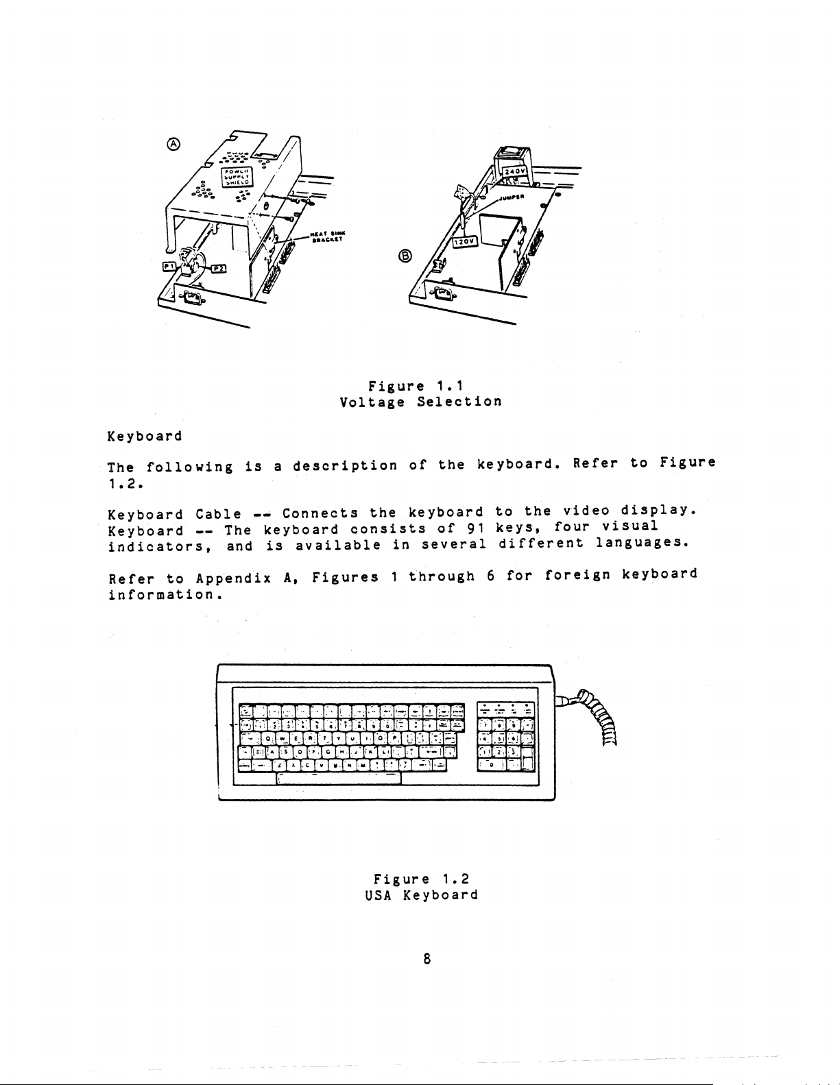
Keyboard
The
following
1.2.
Voltage
1s a description
Figure
of
1.1
Selection
the
keyboard.
Refer
to
Figure
Keyboard
Keyboard
indicators,
Refer
to
information.
Cable
-~
The
and
Appendix
Connects
keyboard
is
available
A,
Figures
the
consists
in
1
Figure
USA
keyboard
of
several
through
1.2
Keyboard
td
91
keys,
different
6
. . . .
-=-
"::"!" ~ -::
t~e
for
video
four
foreign
display.
visual
languages.
keyboard
8
Page 14

Keyboard
Indicators
Refer
POWER
to
ON
properly
KEYBRD
host
OFF
computer
LINE
computer.
CAPS
NOTE:
POWER
LOCK
All
ON
Figure
--
Lights
connected.
LOCK
--
--
Lights
--
LED
(green).
1.3.
Lights
control.
Lights
indicators
when
when
when
power
when
The
the
the
illuminate
.....
is
the
keyboard
keyboard
terminal
CAPS
o
•
.'9"
011
"OC.
ON
and
must
LOCK
red,
•
•
•• C ....
"'IIC
LOCK
the
unit
is
off-line
function
keyboard
is
be
enabled
except
locked
to
from
is
on.
for
is
or
operate.
the
under
host
Keyboard
Refer
The
to
tilt
located
Tilt
Figure
of
at
Adjustment
the
the
rear
1.~.
keyboard
of
LED
can
unit.
Figure
Indicators
be
1.3
adjusted
9
by
pressing
the
two
tabs
Page 15
Figure
Til
t Adj
1.4
ustment
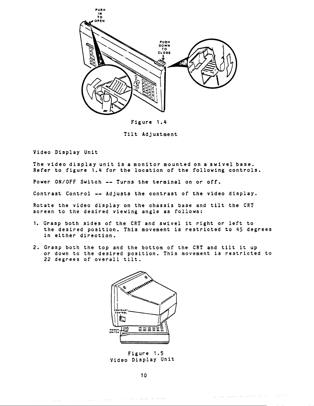
Video
The
video
Refer
Power
Contrast
Rotate
screen
1.
Grasp
the
in
2.
Grasp
or
22
Display
display
to
figure
ONIOFF
Control
the
video
to
the
both
desired
either
both
down
to
degrees
Unit
unit
1.4
Switch
display
desired
sides
position.
direction.
the
top
the
desired
of
overall
is a monitor
for
the
--
Turns
Adjusts
on
viewing
of
the
This
and
tilt.
location
the
the
contrast
the
cha!sis
angle
CRT
and
movement
the
bottom
position.
mounted
of
terminal
as
swivel
of
This
on a swivel
the
following
on
of
the
base
follows:
it
is
restricted
the
CRT
movement
or
and
right
off.
video
tilt
or
and
is
base.
controls.
display.
the
left
to
45
tilt
it
restricted
CRT
to
degrees
up
to
Video
Figure
Display
10
1.5
Unit
Page 16

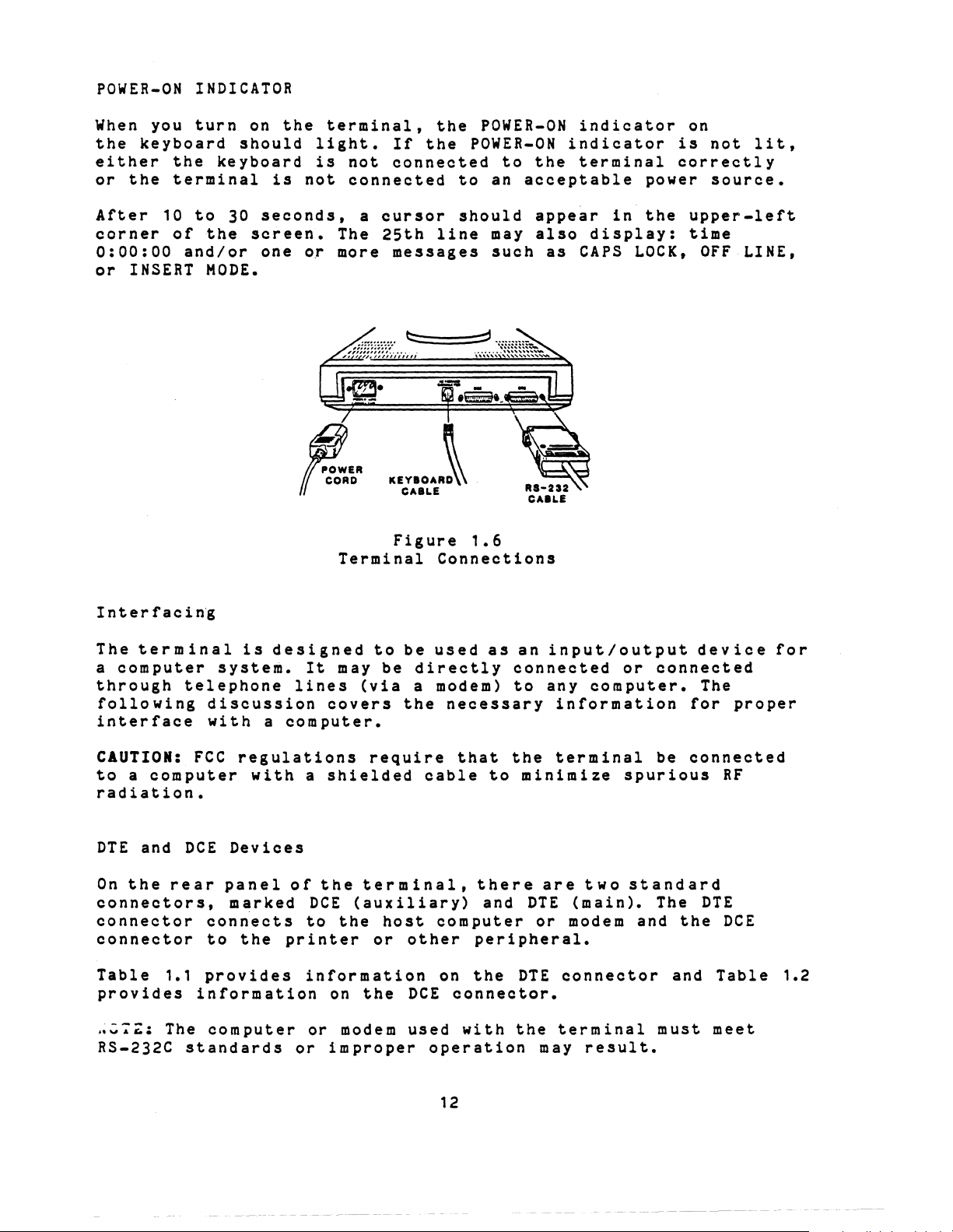
Connections
Place
the
in
Keyboard
the
rear
figure
ClUTION:
telephone
computer
Locate
keyboard
DTE
signals
DCE
RS-232
NOTE:
securely
When
RS-232
computer's
for
the
Connector
Connector
signals
Verify
connecting
cable
the
video
is
facing
1.6.
Connector
The
coiled
cord.
to
the
coiled
connector
to
a modem
that
or
improper
into
DCE
proper
display
you.
cable
Do
not
telephone
keyboard
on
(Main)
(Auxiliary)
to
the
connector
connector).
--
and/or
data
the
operation
terminal
the
on a
The
Provides
assembly
attempt
system
the
rear
Provides
computer.
--
terminal
DTE
and
DTE
connector
(refer
solid
terminal
cable.
Provides
DCE
directly
the
to
connect
or
Connect
of
the
the
devices
cable
of
the
to
work
resembles
the
surface
connections
necessary
damage
video
necessary
the
or
connections
terminal
to
a
and
the
computer
and
signals
a
conventional
the
keyboard
could
the
cable
display.
ElA-standard
necessary
a
printer.
may
computer,
other
hardware
turn
are
illustrated
for
or
result.
to
the
EIA-standard
are
result.
plug
end
into
it
until
the
RS-232
tightened
the
the
manual
keyboa
When
into
connector
connector).
When
(HE-134-1454)
manual
auxiliary
both
primary
POWER
to
After
cable
terminal's
Turn
Plu~
lAC
connecting
the
DTE
connecting
for
(DCE)
ports,
(DTE)
LINE
the
terminal.
verifying
into
the
video
the
power
receptacle);
(refer
the
connector
to
the
may
the
proper
connector.
the
printer
port
Connector
that
the
power
base
unit.
display
cable
then
terminal
the
terminal
have
for
--
the
connector
into
to
and
the
modem
to
connection).
must
the
Connects
power
until
press
hardware
to
be
used
Since
operate
host
the
an
appropriate
the
a modem,
other
a
printer,
(refer
Plug
the
baud
computer.
1'5V
switch
located
front
power
end
manual
the
at
the
power
is
on
is
switch
plug
into
a
to
the
rate
off,
the
facing
power
the
the
for
null
printer
printer
setting
same
source
plug
rear
source
to
ON.
RS-232
modem's
the
modem
cable
baud
via
the
of
you.
cable
(DCE)
proper
cable
hardware
into
applies
rate
power
power
the
as
the
to
the
cord
"
Page 17
POWER-ON
INDICATOR
When
the
keyboard
either
or
the
After
corner
0:00:00
or
INSERT
you
turn
the
terminal
10
to
of
and/or
on
should
keyboard
30
seconds,
the
screen.
one
MODE.
the
terminal,
light.
is
is
not
The
or
more
~
fp:O~D
..
Terminal
If
not
connected
connected
a
cursor
25th
messages
•• n •••
Figure
the
the
to
should
line
~
CABLE
Connections
POWER-ON
POWER-ON
to
the
an
acceptable
appear
may
also
such
1.6
as
CABLE
indicator
indicator
terminal
in
display:
CAPS
LOCK,
on
is
correctly
power
the
upper-left
time
not
source.
OFF
lit,
LINE,
Interfacing
The
terminal
a
computer
through
following
interface
CAUTION:
to
a
radiation.
DTE
On
the
connectors,
connector
connector
Table
provides
~~7~:
RS-232C
telephone
computer
and
DCE
rear
1.1
The
standards
is
designed
system.
discussion
with
FCC
connects
to
provides
information
computer
a
regulations
with
Devices
panel
marked
the
printer
It
may
lines
computer.
a
of
DCE
to
information
or
or
(via
covers
shielded
the
terminal,
(auxiliary)
the
on
the
modem
improper
to
be
be
directly
a modem)
the
require
host
or
other
DCE
used
used
cable
computer
on
operation
as
necessary
that
to
there
and
peripheral.
the
connector.
with
an
input/output
connected
to
any
information
the
terminal
minimize
are
two
DTE
(main).
or
modem and
DTE
connector
the
terminal
may
result.
or
connected
computer.
be
spurious
standard
The
must
device
The
for
proper
connected
RF
DTE
the
DCE
and
Table
meet
for
1.2
12
Page 18
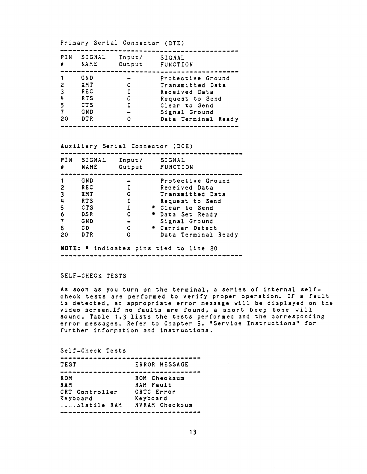
Primary
-------------------------------------------
PIN
#
-------------------------------------------
,
2
3
4
5
7
20
Serial
SIGNAL
NAME
GND
XMT
REC
RTS
CTS
GND
DTR
Connector
Inputl
Output
o
I
o
I
o
(DTE)
SIGNAL
FUNCTION
Protective
Transmitted
Rec
e i
ved
Request
Clear
Signal
Data
to
to
Ground
Terminal
Ground
Data
Data
Send
Send
Ready
Auxiliary
PIN
,
--------------------------------------------
1
2
3
4
5
6
7
8
20
HOTE:
SELF-CHECK
As
check
is
video
sound.
error
further
SIGNAL
NAME
GND
REC
XMT
RTS
CTS
DSR
GND
CD
DTR
soon
detected,
Serial
Input/
Output
*
indicates
TESTS
as
you
tests
screen.If
Table
messages.
are
an
1.3
infor~ation
Connector
I
o
I
I
•
o
o
*
o
pins
turn
on
performed
appropriate
no
faults
lists
Refer
to
and
(DCE)
SIGNAL
FUNCTION
Protective
Received
Transmitted
R e
que
s t t 0
Clear
• 0 a t a Se t
Signal
Carrier
Data
tied
the
are
the
Chapter
instructions.
to
Terminal
to
terminal,
to
verify
error
found,
tests
Ground
Data
Data
Se
Send
Rea
d y
Ground
Detect
line
20
message
performed
5,
"Service
n d
Ready
a
series
proper
a
short
will
of
internal
operation.
be
beep
and
the
Instructions"
self-
If
a
displayed
tone
corresponding
will
for
fault
on
the
Self-Check
TEST
ROM
RAM
CRT
Controller
Keyboard
.,_
...
.;,latlle
Tests
RAM
ERROR
ROM
RAM
CRTC
Keyboard
NVRAM
MESSAGE
Checksum
Fault
Error
Checksum
13
Page 19

/
Page 20

Chapter
2:
General
Information
Theory
The
following
the
terminal's
Refer
US[~
......
~ILI.EL£
~":'.£ L I'.r--~
of
to
Operation
paragraphs
major
Figure
!xPAIo;S
D
2.1,
IO~.
soon
OR
u
~
OC
P.
H'
OR
',\0:;'('.,
~OCK[l
provide
assemblies.
the
overall
a
block
block
diagram
diagram.
Ii
CO,:lROtL[P
description
I
D!O
of
CDI.'
(K
P~OC'~·.~
RO~1
115
BYT[S
UA1
C[UCH£D
K!YBOU:
\~
IT
!~cor·I·.c.
M
IOCIC
Figure
Overall
Block
2-1
Diagram
UlRl&UT[S
co,.
TAOLLE~
1
Page 21
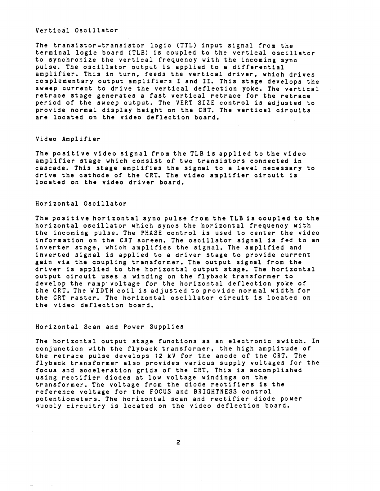
Vertical
The
transistor-transistor
terminal
to
synchronize
pulse.
Oscillator
logic
The
oscillator
amplifier.
complementary
sweep
retrace
period
provide
are
current
stage
of
normal
located
the
This
output
to
generates
sweep
on
board
the
vertical
in
turn,
drive
display
the
video
(TLB)
output
feeds
amplifiers
the
a
output.
height
deflection
logic
is
coupled
frequency
is
the
vertical
fast
vertical
The
on
(TTL)
applied
vertical
I
and
deflection
VERT
the
board.
input
to
with
to
II.
retrace
SIZE
CRT.
signal
the
the
a
driver,
This
control
The
from
vertical
incoming
differential
which
stage
yoke.
for
the
is
vertical
the
oscillator
sync
drives
develops
The
vertical
retrace
adjusted
circuits
the
to
Video
The
Amplifier
positive
amplifier
cascade.
drive
located
the
on
Horizontal
The
positive
horizontal
the
incoming
information
inverter
inverted
gain
driver
output
develop
the
the
the
via
is
circuit
CRT.
CRT
video
the
raster.
video
stage
This
stage
cathode
the
Oscillator
horizontal
oscillator
pulse.
on
stage,
signal
the
coupling
applied
ramp·
The
WIDTH
deflection
which
of
video
the
which
is
to
uses
voltage
The
signal
consist
amplifies
the
driver
which
The
PHASE
CRT
screen.
amplifies
applied
transformer.
the
a
winding
coil
is
horizontal
board.
from
of
the
CRT.
The
board.
sync
pulse
syncs
control
The
to
a
horizontal
on
for
the
adjusted
oscillator
the
TLB
two
Signal
video
from
the
oscillator
the
signal.
driver
The
output
the
horizontal
to
is
applied
transistors
to
a
amplifier
the
horizontal
is
used
The
stage
output
stage.
flyback
deflection
provide
circuit
to
connected
level
circuit
TLB
is
coupled
frequency
to
center
signal
amplified
to
provide
signal
The
transformer
normal
is
the
video
necessary
is
the
is
fed
and
current
from
the
horizontal
to
yoke
width
located
in
to
with
video
to
of
for
on
to
the
an
Horizontal
The
horizontal
Scan
conjunction
the
retrace
flyback
focus
using
transformer
and
acceleration
rectifier
transformer.
reference
voltage
potentiometers.
~uooly
circuitry
output
with
pulse
The
and
Power
the
develops
also
diodes
voltage
for
The
horizontal
is
stage
flyback
grids
at
from
the
located
Supplies
functions
transformer,
12
kV
provides
of
low
voltage
the
FOCUS
on
for
the
and
scan
the
2
as
the
various
CRT.
windings
diode
rectifiers
BRIGHTNESS
and
rectifier
video
an
electronic
the
high
anode
of
supply
This
is
on
control
deflection
switch.
amplitude
the
CRT.
voltages
for
accomplished
the
1s
the
diode
power
board.
In
of
The
the
Page 22

DETAILED
CIRCUIT DESCRIPTION
This
section
keyboard
the
power
KEYBOARD
Refer
to
following
NOTE:
The
represent
device's
The
keyboard
single-chip
and
a
timer
the
status
provides
matrix
under
for
All
keys
control
more
the
comprise
eleven
diode
scan
are
generation
The
port
lines
the
line,
of
selected
the
keyboard.
the
eight
port
0
bits
provides
assembly,
supply.
ASSEMBLY
the
keyboard
paragraphs.
symbols
the
logic
design.
assembly
microcomputer
US.
U1
indicator
serial
communication
are
of
information).
keys
a
matrix
except
lines
placed
of
phantom
2
bits
the
1
of
scan
sense
lines
Resistors
sense
AO
through
terminal
on
flow
performs
LED(s),
scanned
U1
(refer
RESET
keyboard
or
an 8 x
at
each
CO
(LSB)
16
decoder
line
R11
lines.
a
detailed
assembly
the
schematics
of
contains
U1, a 1
utilizing
to
BREAK,
consisting
crossover
key
signals
through
being
are
checked
through
The
active-low
A7.
circuit
logic
board,
schematic
the
circuit
an
8 x
to
keyboard
enables
with
a
data
sheets
CTRL,
l'
configuration.
point.
due
C3
U2.
The
driven
for
R18
in
11
16
matrix
the
the
strobe
of
to
(MSB)
port
low.
a
serve
sense
description
video
as
this
rather
matrix
circuit
you
read
service
than
keyboard,
decoder/multiplexer
scanning,
timer
terminal
for
logic
beeper
scanning
on
the
8021
and
the
two
SHIFT
eight
The
multiple
of
2
After
key
as
sense
A
keyswitch
diodes
U1
control
bits
selecting
closure
pullup
lines
key
drive
on
resistors
are
of
the
board,
the
manual
any
specific
a
U2,
controls
T1,
board.
The
technique
microcomputer
keys
lines
and
and
prevent
the
closures.
the
scan
U2
with
a
scan
the
matrix
read
by
and
and
for
RESET
The
active-low
These
keys
and
The
NORed
input
R19
keys
to
input
output
together
of
and
resetting
hardware
inputted
of U 1.
The
chip
sen~
the
to
line
BREAK,
keys
all
send
to
unique
port
of
U1
via
capacitor
U1.
reset
directly
U4D
buffers
the
keyboard)
pullup
CTRL,
utilizing
have
the
by
the
The
of
resistor.
special
keycodes.
1
(Bn
SHIFT
U3A.
RC
C8
provide
output
the
to
port
the
to
and
the
pullup
functions
of
keyes)
The
output
network
of
U3A
terminal.
1 (B2) and
data
input
Port
two
resistors
The SHIFT
U1.
and
of
composed
a
minimum
is
The
stream
T1
of
1 (B3)
3
SHIFT
and may
RESET
U3A
reset
also
RESET
the
(RCV)
U1.
outputs
keys
are
R8, R9, R10,
be
keys
of
are
BREAK
is
applied
R19
key
and C8.
pulse
buffered
BREAK
CTRL
key
Signal
Resistor
the
direct-drive,
used
ORed
with
together
are
to
width
by
U4E
key
also
to
port
(serial
R22
serves
serial
and
R21.
other
logically
the
RESET
Resistor
for
for
is
1
(80)
data
data
as
Page 23

generated
logic
A
for
board.
3.579
the
drives
Resistors
timer
OFF
U4B,
LEOs
interval.
LINE,
and
02, 03,
(POWER
and
D4
terminal
of
power
by
MHz
internal
timer
R1
and
U4C.
ON)
are
logic
to
the
Resistor
crystal
circuit
and
KEYBRD
Resistors
and
fed
turned
the
keyboard
is
control
R2
and
Port
04.
directly
on
board.
keyboard
R23
connected
and
US
for
capacitor
1
bits
LOCK
R4, R5,
Resistor
from
by
U1
The
assembly.
(XMT)
serves
via
as
between
timing
the
piezoelectric
B4, B5, and
LED
indicators
and
R7
is
the
+5
in
response
LED
01
is
buffer
the
references.
cg
are
R6
are
the
volt
to
turned
U4-F
line
pullup
XTAL 1 and
beeper
selected
B6
drive
via
the
bias
bias
line.
resistor
The
commands
on
by
to
the
resistor.
XTAL 2 of
The
port
to
set
the
CAPS
buffers
resistors
LEDs
from
the
application
terminal
1
T1.
the
U4A,
for
D2,
the
bit
LOCK,
for
LED
03,
U1
B7
01
Approximately
through
+5
volts
pin
DC
Capacitors
volt
connector
TERMINAL
Refer
following
Power-Up
To
being
reset
pressing
The
0401,
circuit
C416
of
pulls
(Vcc)
to
set
the
changed
can
power-up
resistors
U406C. When
is
in
NAND
gate
this
ground
LOGIC
the
paragraphs.
and
be
the
microcomputer
C416
inputs
output
charg~&"th~ough
for
allows
+9.4
8
to
with
C3
through
to
the
BOARD
terminal
Reset
terminal
by
initiated
SHIFT
reset
R408
a
discharged
U406C
output
U433
U406C
U433
volts
voltage
C1
and
C7
keyboard's
pins
are
logic
Circuit
back
software
either
and
RESET
circuit
and
the
low
voltage
resets.
resistor
to
become
to
exit
DC
is
regulator
C2
used
and
C10
integrated
1
and
board
to
its
escape
keys
for
R423,
terminal
condition.
and
the
to
a
After
high;
the
applied
as
provide
U5.
line
to
US
filter
decoupling
circuits.
3.
schematic
original
operating
sequences,
by a power-up
on
the
the
terminal
capacitor
is
This
output
level
this
R408.
thus
reset
first
This
C416,
holds
(pin
that
initial
action
the
condition.
the
keyboard
regulates
capacitors.
as
you
U433
or
by
keyboard.
consists
and
turned
one
8)
high.
insures
reset,
causes
resulting
assembly
the
output
for
the
The
keyboard
read
mode
must
be
the
after
reset.
simultaneously
of
diode
integrated
on,
capacitor
input
(pin
Resistor
that
capacitor
both
low
at
to
+5
A
10)
R423
its
Simultaneously
also
terminal,
power
resets
up,
the
capacitor
immediately
the
same
input
to
function
U406C.
sufficient
operate
properly.
preSSing
U433.
probability
begins
to
override
Since
C435
to
charge
as
the
Capacitor
When
the
two
of
is
capacitor
C435
the
reset
the
SHIFT
SHIFT
keys
have
accidental
in
a
discharged
through
finally
condition
and
4
and
and
RESET
to
be
reset
resistor
resistor
charges
RESET
keys
actuated
is
condition,
R425.
on
to
and
allows
keys
are
on
the
to
minimal.
but
This
the
other
a
level
U433
keyboard
reset
the
At
performs
that
to
is
Page 24
simultaneously
pin
2)
causes
discharges
the
terminal.
protected
accidentally
The
low
that
also
(U427).
inverted
reset
Resistors
pulses
composed
less
keys
down
applied
Since
by
input
R425
that
of
than
the
together.
to
initiate
capacitor
to
a
Because
from
unplugged
is
as
the
U~25D
is
could
R401,
time
pressed,
TTL
low,
a
false
sent
the
clear
enable
before
pulled
and
R401
otherwise
R425,
it
This
reduces
the
the
reset
from
to
low,
takes
reset.
a
logic
C435
the
reset
the
input
input
it
and
and
low
to
discharge.
output
lines
1n
the
the
video
reset
to
to
is
applied
the
screen
capacitor
reset
C435
to
actually
the
time
from
of
event
circuit
the
U~27
the
forms
the
U406C
float
that
display
from
video
is
to
is
blanked
C435
terminal.
a
time
press
the
two
keyboard
Once
goes
high,
the
unit.
the
suppression
pulled
the
data
integrate
constant
the
keys
this
high
the
keyboard
keyboard
high
input)
during
The
SHIFT
must
(plug
capacitor
and
terminal
circuit
(and
reset.
any
noise
network
that
and
be
P~03
resets
is
is
and
is
RESET
held
is
the
After
begin
display
Serial
The
asDTE
DCE
connect
can
a
reset
the
RAM
Ports
terminal
(Data
(Data
the
be
connected
initialization
Computing
Microcomputer
This
terminal
for
for
IC
contains
to
an
asynchronous
linking
protocols.
U433
reading
serial
responds
or
IIO
-pa<t.
writing
communications
terminals,
port
overrun,
receiver's
Since
double
contains
which
U433
buffer,
interrupt
can
is
complete,
and
initializes
has
two
Terminal
terminal
to
U433
controls
a
built-in
communicate
peripheral
to
a
serial
to
provides
with
printers,
two
buffers
could
usually
only
firmware
routine.
the
RS-232
compatible
Equipment),
Equipment).
to
a
computer
a
printer.
the
serial
with
other
communications
devices
port
the
serial
using
interrupt
asynchronous
standard
or
computers.
occur
before
to
eliminate
if
the
UART
the
maintain
one
buffer
is
causes
This
two
CRT
and
the
The
DTE
or
modem
operation
port
peripherals,
element.
standard,
port's
modes
devices,
The
CPU
fails
beginning
the
transmit
used
U433
clears
controllers.
ports,
other
port
is
while
of
which
This
request
buffer.
to
such
receiver
the
possibility
to
of
the
link
at
the
to
the
scratch
one
is
configured
is
configured
normally
the
the
serial
enables
without
port
asynchronous
by
either
This
full-duplex
facilitate
as
other
input
respond
next
without
transmitter
used
DCE
ports.
the
the
is
useful
to
this
of
to
frame.
pad
and
as
to
port
need
the
a
output.
In
the
on
the
samples
asynchronous
received
taken
frames.
near
modes,
the
false
For
center
noise
of
start
rejection,
each
5
bit
rejection
received
a
majority
bit
is
must
provided
of
three
agree.
Page 25

The
1/0
operation
port
modes
may
be
programmed
as
follows:
to
function
in
any
of
the
four
Mode
o
1
2
3
Proper
transmission
of
upon
uses
U433's
divided
in
TH1
software).
transmission
are
7200,
The
U433, a
line
timing
transmission
the
transmission
clock
by
if
75.
110. 150,
9600,
hardware
2-line
driver
Synchronous
CMOS
UART
variable
UART
variable
UART
variable
for
rate
operating
frequency.
12
(or
counter
This
rate.
and
required
to
(U442),
shift
interface
transmission
interface
~ransmission
interface
transmission
the
serial
generator
rate
generation
mode
mode
the
T1
1
is
configured
frequency
The
300.600,
19200
baud.
to
1-line
and a
Operation
1/0
expanslon
registers.
with
with
with
inside
of
the
1,
the
In
this
input
is
then
baud
rates
1200.
complete
output
quadruple
10-bit
rate.
l1-bit
rate.
ll-bit
rate.
1/0
data
U433.
are
possible
serial
transmission
mode,
is
in
the
divided
the
divided
that
1800.2000.2400,3600.4800,
the
multiplexer
ltne
using
frame
frame
frame
is
provided
Three
port.
Since
rate
oscillator
by
auto-reload
by
this
terminal
serial
receiver
TTL
or
and
and
and
different
and
are
is
256.
32
to
link
(U431),
by
a
dependent
this
terminal
generated
frequency
minus
mode
provide
will
consists
a
quadruple
(U429).
methods
the
value
by
the
support
of
from
is
Pin 4 of
U433.
the
this
When
auxiliary
line
computer
The
transmit
on U433
these
the
high
OR
port
regardless
Therefore.
transmits.
OR
gate
to
be
transmitted
select
The
clear
Signals
to
the
terminal
Signal
multiplexer
this
is
a
port
line
through
gates
s~le-ct·
when
When
U4430
bit
on
line
is
to
send
the
drivers.
.is
ready
detect
line
port
logic
to
the
drivers
an
is
from
bit
of
the
the
high
because
low,
OTE
OTR.
(RLSO)
U431
is
to
0,
the
is
logic
receive
U431
receive
are
OR
gate
the
is
high,
the
logic
port
port
select
~elect
regardless
of
the
OTE
(CTS) and
port
On
data
are
the
set
signals
connected
1,
sends
pin
tied
(U443C
port
select
the
level
bit
bit
inverter
port
transmits.
data
taken
auxiliary
ready
are
6
U431
pin
sends
of
data
of
U433's
directly
or
U4430).
output
of
the
is
is
of
the
terminal
directly
port,
(DSR),
all
tied
to a latched
data
U433's
received
serial
to
The
bit
(UQq8,
of
the
data
a
logic
a
logic
logic
UqqqC.
level
Thus
ready
from
the
and
the
together.
received
serial
from
port.
the
transmit
second
pin
OR
gate
to
be
1,
the
0,
the
when
(OTR)
U433
CTS,
received
1/0
pin
from
port.
the
input
7).
When
UQ43
transmitted.
OCE
port
output
of
the
data
the
control
and
passed
data
on
When
pin
to
is
of
port
line
Page 26

Another
P r i n t "
DTE
mod
port
printer.
U432,
be
pin
enabled.
applied
7.
CPU
and
The
main
U433
U433
access
five-source
chip
serial
the
logic
and
contains
memory
oscillator/clock
channel.
total
board
feature
e • T
his
to
be
Integrated
1. The
At
from
U432,
Control
timing
its
two-priority
terminal
for
of
the
a
11
0 w s d a t a a r r i v
immediately
circuit
logic
this
time,
pin
Circuitry
and
control
associated
a
4K
x 8
(RAM), 32
circuit,
The
internal
firmware.
installation
serial
channeled
U448,
0
will
handshaking
11
directly
for
circuitry
read-only
I/O
lines,
level
ROM
ports
in g tot
pin
allow
to
the
(ROM,
memory
two
nested
and a high
holds
A
socket
of
additional
is
a
pass
h e
out
the
12
sets
the
pass
from
the
U433,
terminal
RAM,
(ROM), a 128
16-bit
interrupt
performance
approximately
is
included
firmware.
through
't
e r
min
a 1
DCE
port
a
logic
through
DCE
port
pin
is
established
and
control
timer/counters,
structure,
on
or
"Blind
fro m the
to
a
1
or 0 to
operation
will
logic).
x 8
random
full-duplex
one-half
the
terminal
by
an
to
be
a
on-
of
The 32
I/O
open-drain
bidirectional
separately.
Port
order
this
0
--
address
terminal
circuitry
respective
100
nanoseconds
goes
applied
the
Port
1)
riSing
is
low.
1
--
used
to
keyboard.
line
are
RFI
Bit
0,
allows
by
This
logical
the
15
setup.
all
from
buffered
suppresst'on.
2 (U433
this
bit
the
U433,
feature
rows
screen
minutes
This
RAM,
lines
bidirectional
I/O
Port
0
lines.
do
must
demultiplex
buses.
The
low
address
edge
Port
as
Bit
the
1
the
1 (U433
keyboard
by
pin
inverted
video
this
bit
is
of
saver
of
inactivity
bit
including
are
divided
ports.
functions
Since
not
have
The
address
later,
at
the
this
latch
of
the
is
a
general
handshake
pin
to
U425B
3)
is
and
used
by U425D,
to
be
displayed.
causes
particularly
video
in
operation,
blanks
the
video
port,
Each
as
the
on-chip
the
address
pin
U441,
signal
2)
the
U425F,
as
the
SO
if
screen
RAM
into
of
the
memory
exits
is
(ALE).
purpose
line
is
terminal
the
video
useful
Hz
where
this
is
four
while
the
ports
ports
multiplexed
address
address
at
latch
inverted
where
the
between
used
as
respectively,
video
is
connected
When
information
in
operation.
the
feature
during
being
a-bit
1, 2 and
will
and
peripheral
latching,
and
data
port
0
enable
by
address
I/O
port.
the
terminal
the
input
logic
enable
to
toggled
blanking
It
is
screen
is
a
manual
is
enabled
initialized.
ports.
be
data
lines
and,
(U433,
U444B
is
Bit
board.
and
bit.
U427
to
to
the
also
turned
Port
3
are
0
is
described
bus
and
low
devices
U433
onto
their
approximately
pin
30)
before
latched
0 (U433
and
it
on
pin
the
communications
These
filtered
When
pin
logic
be
inhibited.
extra
used
in
reset,
lines
for
at
logic
13
and
1
(high)
unused
during
off
after
terminal
while
an
in
is
7
Page 27

Bit
3 (U433
volts,
the
logic
has
Bit
t
his
bit
is
1
(high),
been
4 (U433
handshaking
connector
Bit
5 (U433
handshaking
connector
Bit
6 (U433
Pr
int"
Bit
the
For
bits,
refer
logic
mode.
7 (U433
video
further
the
to
board
pin
4)
bit
in
pulled
information
pressed
pin
5)
at
the
P402
pin
at
through
6)
the
P402through
pin
7)
pin
8)
circuit
information
video
the
enable
applicabl~
circuit
is
used
h i
bit s the
up
by
firmware
is
ignored.
functions
computer
functions
computer
line
functions
is
used
(U403
bit,
descriptions.
as
an
S E
from
as
OTE
line
driver
as
OTE
driver
as
as
a
pin
1).
regarding
and
paragraphs
output.
TU
P mod
and
the
the
port
the
port
the
initial
the
the
eke
recognized
keyboard
OTR
signal
and
U442B.
CTS
signal
and
U442A.
RTS
input
synchronization
keyboard
RS-232
in
the
When
jumpered
y v i a
that
for
is
applied
for
is
applied
in
communication
handshaking
keyboard
to
firmware.
as
being
the
proper
to
port
proper
to
port
the
"Blind
or
the
+5
at
SET
signal
bits,
terminal
When
a
UP
key
to
Port
order
2
--
address
combination
Port
and
serial
3
--
1 (U433
port
asynchronous
asynchronous
Bit
2 (U433
character
indicates
data.
5
transfer
Bit
The
is
inverted
3 (U433
at
character
indicates
been
Bit
Used
handled.
4 (U433
as
an
instruction
video
memory
Port
byte
of
Port
pins
circuitry.
receive
transmit
pin
CRT
controller
that
logic
the
pin
CRT
controller
the
pin
output,
to
via
2 (U433
ports
3
1s
10
12)
a
row
1
level
at
gate
two
13)
last
14)
the
become
OMA.
pins
when U433
0
and
used
and
Bit
data
as
11,
0
input,
data
is
used
(U418).
buffer
buffer
U401F.
CRTCs.
is
used
(U418).
display
is
also
bit
causes
20H.
This
21
to
28)
accesses
2
form
a
general
the
respectively)
functions
while
output.
as
the
interrupt
A
logic
is
ready
ready
This
as
row
an
A
and
interrupt
interrupt
logic
connected
the
is
for
signal
last
value
used
is
used
external
total
purpose
are
as
the
bit
1
0
level
the
0
level
retrace
to
the
to
quickly
only
memory.
16-bit
IIO
part
serial
functions
0
input
loading
(BRDY)
initiates
1
input
character
video
of
the
for
address
port.
of
at
this
from
from
for
circuitry.
jammed
clear
the
The
Bits
the the
port
as
from
of
character
U418
a
OMA
this
higher
the
the
port
the
bit
has
DMA
a
row
bus.
0
bit
pin
of
8
Page 28

Bit
5
request
the
PRT
(U433
to
CTRL
pin
send
signal.
15)
(RTS)
is
used
Signal
as
from
an
input
the
to
the
selected
serial
port,
port
as
depending
the
on
Bits
for
The
U433
during
6
and
transferring
PSEN
(pin
normal
internal
U433
receives
information
computer.
converts
attribute
provided).
attribute
U446
with
directly
The
attribute
to
the
four
After
writes
(U436).
placing
the
The
enables
(U428)
are
so
connected.
associated
location
7 (U433
signal
29).
fetch
program
character
from
When
it
to
data
U433
display
the
connecting
data
possible
the
character
20K
the
memory
that
attribute
equivalent
pins
data
is
the
It
enables
operations
memory.
either
a
key
character
associated
then
memories
16K
address
the
is
att~ibute
address
chip
the
secondary
The
microcomputer
to
16
bytes
program
the
data
the
is
pressed,
data
with
sends
the
Signal
attribute
a
four-bit
attributes.
data
out
signal
select
data
a
in
video
and
17)
between
store
external
versus
and
keyboard
and
the
attribute
(U~37
data
to
and
and
data
display
screen
are
port
enable
attribute
interface
the
keyboard's
sends
character
and
U438)
and
the
bus
wide
1n
the
the
character
the
the
bus
and
places
memory
the
WR
0
and
output
program
using
it
the
to
data
data
by
write
to
the
primary
nibble
(DO -D3)
display
write
Signal
bidirectional
the
the
character
chips
position.
and
RD
signals
the
data
control
memory
to
microcomputers
or
the
host
microcomputer
the
terminal
already
to
the
enabling
Signal
(WR),
data
memory,
display
memory
from
bus
primary
data
and
in
an
used
bus.
from
the
bus
(the
bus
buffer
and
bus.
applicable
U433
then
U433
driver
bus
address
(U1)
After
appropriate
character
their
This
is
Memory
Figure
through
well
U433
corresponding
operation
described
Map
2.2
A12
as
other
has
memory,
display
in
depicts
are
circuits.
placed
occurs
selector/demultiplexer
map.
the
this
memory
CRT
by
the
video
the
connected
display
data
and
the
controller
way
of
display
terminal's
to
the
Chip
and
U423
selects
must
attribute
direct
9
data
be
transferred
(U418
circuit
memory
memory
is
a
4K
increments
in
the
display
and
memory
description.
map.
select
3-input
from
U419,
access
Address
circuit
to
8-output
of
the
memory
to
respectively).
(DMA),
lines
(U423)
data
the
memory
which
A15
as
Page 29
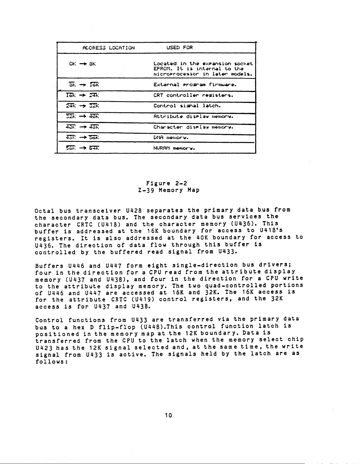
ADCRES~
LOCATION
tr,X;C
FOR
m
m
321<
~
Q:
~
Octal
the
character
buffer
registers.
U436. The
controlled
bus
secondary
is
01<
-+
SK
-,.
~~
m
~
~
~~
-+
~
-+~
~
:'0,(
-+
04
transceiver
data
CRTC
addressed
It
direction
by
....
bus.
(U41S) and
at
is
also
of
the
buffered
Locat.
EPROI'1.
mi
Ext.oiPrnal
CRT
Cor,t.rol
At.t.ribut.e
Charilc·t.er·
[.INA
HVRFtM
Figure
Z-39
U428
The
separates
secondary
the
the
16K
addressed
data
flow
read
.. d in
It.
c·rOF·"·OCEoS
P"'OViIIII
cont.roll.,.
sisnal
melllor"".
mefl'or·
2-2
Memory
character
boundary
at
the
through
signal
t.he
t.
.or
di.pl
di
SP
...
Map
the
data
expansion
ir,t.",,·nal
lat..,.
in
1'i
rlTtW¥'oiP.
r.Slist..,.
latch.
...
""
"
....
l·iiI·~
It
...
primary
bus
memory
for
40K
boundary
this
from
sock.t.
ti'";.
t.o
modeh.
...
mor"ll.
I'I,c:.r'ol.
services
(U436).
access
buffer
U433.
data
to
bus
for
is
from
the
This
U418's
access
to
Buffers
four
memory
to
of
for
access
in
the
U446
the
(U431
attribute
is
Control
bus
to
a
positioned
transferred
U423
signal
has
from
follows:
U446
the
and
direction
and
and
U441
attribute
for
functions
hex
D
in
from
the
12K
U433
U441
U438),
display
are
CRTC
U431
from
flip-flop
the
memory
the
signal
is
form
for a CPU
and
accessed
(U419)
and
U438.
U433
CPU
selected
active.
eight
read
four
in
memory.
at
control
are
transferred
(U448).This
map
at
the
to
the
latch
The
signals
10
single-direction
The
16K
from
the
two
and
the
direction
quad-controlled
32K. The
registers,
via
control
12K
boundary.
and,
when
at
the
the
held
attribute
for
and
the
function
memory
same
by
time,
the
bus
16K
the
primary
Data
latch
drivers;
display
a
CPU
portions
access
32K
latch
is
select
the
are
write
is
data
is
chip
write
as
Page 30
Signal
EAROMSTORE
When
setup
ROM
if
the
setup
Description
this
information
portion
terminal
information
bit
of
is
the
set,
is
EAROM.
is
powered
remains.
the
stored
current
in
the
Therefore,
down,
the
B1
PRT
CNTL
EAROMRECALL
PASSTHRU
The
character
further
in
the
the
chip
CLOCK
accessed
following
WR
or
select
CIRCUIT
RD
When
attribute
This
between
ports.
When
stored
EAROM
and
This
the
print
display
signals
signal
this
bit
controls
the
this
in
is
brought
is
ready
is
an
control
operation.
memory
at
28K
as
paragraphs.
(U443A
required
bit
is
activated.
auxiliary
bit
the
to
IIO
of
DMA
or
to
is
set,
is
set,
ROM
into
use.
bit
the
and
memory.
The
U408A)
access
the
the
selection
and
the
portion
the
that
pass
the
attribute
28K
signal
blink
computer
information
of
RAM
is
used
through
This
to
produce
the
NVRAM
the
portion
for
display
is
discussed
is
ORed
at
the
low
(U439).
memory
further
U426D
level
are
with
The
main
operations
that
Crystal
a
14.784
undesired
to
the
C428
Inverter
provides
the
clock
used.
into
The
buffered
circuit,
synchronization
fed
directly
This
rate.
(U424A)
oscillator
is
biased
Y401
MHz
input
and
C441
lJ.41.1D
the
This
other
the
allows
In
the
divides
negative
circuit.
prevents
for
the
by
provides
clock
and
provide
buffers
necessary
circuits.
14.784
main
circuits.
to
the
the
video
main
the
clock
terminal.
resistors
positive
signal.
feedback
altering
impedance
The
the
MHz
processor
clock
dots
processor
14.784
circuit
Decoupling
the
the
high
current
other
high
clock
In
input
to
MHz
It
consists
R411
from
buffers
frequency
clock
the
clock
and
feedback
being
oscillator
matching
frequency
drive
signal
dot
of
be
shifted
Signal
1 1
controls
R412
capacitor
introduced
for
internal
signal
is
circuit,
clock
shift
circuit,
by
all
of
an
for
so
the
frequency.
for
the
clock
the
remaining
from
coupled
and
cirCUit,
register
out
at
a
D-type
a
factor
of
the
inverter
linear
inverter
C439
from
crystal
signal
to
U411
to
the
the
of
timing
operation.
prevents
the
Capacitors
and
portion
are
being
the
dot
video
the
signal
U415.
14.784
flip-flop
2
(U411A)
generates
output
circuit.
not
coupled
clock
timing
MHz
of
and
is
Page 31

to
produce
signal
which
8
for
divides
use
divided
U418
is
and
used
character
a
7.392
path
is
to
the
in
the
by 8 signal
U419
where
because
cell.
video
it
MHz
processor
the
counter
14.784
timing
is
fed
it
is
matches
MHz
directly
used
the
clock
integrated
signal
and
synchronization
as
the
eight
signal.
circuit
by a factor
to
CRT
controllers
character
horizontal
The
of
clock.
video
remaining
(U403),
2,
4,
circuits.
This
dots
and
The
signal
per
Integrated
generates
the
shift
from
that
an
the
features
internal
triggering
timing
the
In
divided
to
screen
addition,
by
generation.
CHARACTER
The
main
is
formed
character
type
the
U419,
of
integrated
attribute
however,
character
the
same
unnecessary.
circuit
a
signal
register
character
synchronous
look-ahead
of
these
function
refresh
the
7.392
2)
is
ideal
GENERATION
control
by
data
CRT
while
for
controllers
data
allows
by
character
clock
bus,
U404A
that
to
ROM.
is
accept
Chip
carry.
flip-flops
properly.
could
MHz
for
the
U419
circuits
be
in
the
basis.
which
NANOs
used
the
U413
the
to
parallel
is
edge-triggered
The
high
is
necessary
The
14.784
be
programmed
clock
the
rate
processor's
character
U418
operates
used
a
field-defined
for
terminal
Both
makes
special
three
clear
signals
the
a
high-speed
flip-flops,
speed
MHz
for
for
generator
and
U419. U418
on
the
the
terminal
to
use
controllers
synchronization
counter
load
and
for
clock
exactly
the
serial
and
attribute
format.
attribute
from
of
character
Schottky
along
synchronous
the
precise
is
used
50
processor
port
display
operates
data.
require
CRT
controller
data.
are
connected
U403
and
or
baud
and
signal
data
device
with
video
so
that
60 Hz.
(14.784
rate
circuits
on
the
The
that
in
a
to
The
from
five
data
Control
BDRY
BS
CRTC
the
control
bus
is
used
display
lines
both
Line
to
to
determine
RAM
to
that
and
from
Buffer
indicates
ready
data.
and
sent
where
Buffer
enabling
character
buffers.
the
are
the
ready.
for
This
to
it
is
select.
the
when
data
character
used
for
internal
Description
This
that
loading
output
pin
used
An
a
row
of
is
12
to
input
write
data
into
12
should
generating
the
transfer
registers
output
buffer
character
inverted
of
U433,
initiate
signal
signal
the
row
be
signal
is
DMA.
for
transferred
circuitry.
of
data
are:
on
The
the
Page 32

RD
Read
to
input.
read
the
A
control
registers.
signal
used
WR
CS
Initialization
function
a
proper
blinking
position.
All
character
supplied
The
underline
scan
the
line
line
underline
that
then
blink
the
is
until
forces
exclusive
attribute
underline
set.
it
the
information
in
this
rate
then
from
manner
is
controlled
exclusive
the
underline
(underline
visible
through
of
properly.
display
underline.
all
video
data,
from
the
attribute,
in
that
count
bits
outputs
are
the
ORed
information
turns
blink
to
pass
as
ORed
LTEN
and
and
and
block
cursor)
Write
used
control
data
Enables
or
or
the
The
is
as
block.
control
attributes.
two
particular
fed
output
with
is
not
off
line
long
by
(U~1~C)
RVV
cursors.
the
input.
to
write
registers
into
read
write
data.
CRTC's
information
follows:
controllers
if
of
the
to
three-input
low.
the
set.
passes
the
underline
returns
through.
as
the
U~33
pins
enables
underline
the
of
command.
must
and
data.
set
character
CRT
This
blink
or
to
The
blink
and
can
with
of
the
Exclusive
the
by
A
controlsignal
commands
or
row
buffers.
for
status
be
completed
that
type
of
blinking
and
and
synchronization
directly
(active
controller.
output
attribute
if
it
is
through.
and
the
low
blink
at~ribute
be
varied.
the
cursor
CRT
controller
normal
blanking
to
the
to
write
registers
parameters.
before
is
necessary
cursor
block).
(underline.
cursor
synchronization
to
the
high),
cell
to
allows
be
The
NAND
gate
is
inverted
in
an
If
creates
state.
line
U~O~C
at
U~1~B.
off
the
blink
the
allowing
continues
is
The
information
for
ORing
these
video
it
cursor
for
they
for
timing.
pulses
video
the
decoded
LC3.
as
by
blink
blink
to
set.
The
underline
the
two
that
interval.
can
the
home
are
logic.
tenth
through
LCO,
U~07D
If
a
and
high
the
position.
attribute
effect
the
video
toggle
blink
is
coming
signals
to
be
and
Next,
reverse
so
information
logically
lines
during
it
the
information
video
is
~~s~ble
ANDed
from
the
horizontal
in
controller(normally
this
lines
characters
The
video
horizontal
instance,
of
each
video
information
information,
that
and
attribute.
as a blank
that
via
controller.
and
as
it
row.
This
must
the
vertical
is
exclusive
This
character
U~09D
with
vertical
used
for
would
would
c~nnect
must
half-intensity
retrace
disables
line
This
retrace
also
from
now
through
cell.
the
causes
retraces.
blank
not
work
one
be
latched
control
ORed
via
the
the
The
video
inverted
all
The
suppression)
the
well
row
attribute.
signals
U414D
underline
reverse
information
HRTC
video
VSP
first
with
to
the
so
that
with
and
to
output
is
and
graphic
next.
the
and
can
the
information
video
is
VRTC
be
not
last
control
suppressed
of
the
used
scan
reverse
the
be
now
in
Page 33

synchronized.
ORed
This
via
Uij1ijA
informatiort
attribute
signals.
All
of
the
AND
gates
allows
open
be
pull
the
collector
obtained
up
resistors.
The
reverse
to
create
is
and
the
horizontal
video
(Uij02A,
informatiort
a,
circuit
gates
by a resistor
again
C,
to
also
video
the
latched
and
directly
enable
divider
revetse
artd
is
D)
at
drive
output
with
vertioal
now
the
the
network
of
the
video
for
the
half-intensity
retrace
present
same
the
at
time.
video
half-intensity
using
latch
the
the
This
circuit
only
is
exolusive
oharacters.
control
open
collector
timing
board.
attributes
the
The
to
required
Compared
oircuits
controller
row
buffers.
form
the
line A 11
(selects
the
ROM
information
that
is
derived
suppressed
These
three
logically
of
the
shift
attribute
the
ohiin
high
shifts
and
out
shifted
rate,
the
that
li
screen
ne
along
the
fr
equenc
to
the
are
complex.
contain
These
10
address
selects
between
presents
are
by
signals
ORed
register.
or
vertical
of
OR
disables
zeros
at
the
with
to
screen
y.
actual
the
outputs,
from
a
domestio
the
latohed
from
the
blink
with
gat~s,
the
that
main
the
be
refreshed
displays
video
The
charaoter
lines
the
valid
the
are
logically
the
If
or
the
load
translate
clock
timing
character
CCO
through
along
for
the
upper
and
data
into
dot
the
clock.
attribute
clock
any
signal
of
horizontal
load
function
frequency
signals
at
exactly
a
steady
code
with
charaoter
or
lower
a
foreign
on
its
shift
The
or
ORed
the
pin
of
of
into
from
frame
cirouitry,
CC6
outputs
information
the
2K
character
bus.
register
video
the
retrace
together
that
creates
control
retrace)
the
shift
the
video
of
blanks.
1ij.184
the
60
Hz
without
line
count
generator.
of
the
the
eight
on
characters
and
signals
are
active
register
shift
MHz.
controller,
intervals
beating
the
attribute
of
the
coming
outputs,
character
set).
bits
the
control
then
the
load
(the
register.
Dots
This
and
from
Address
Once
of
low
pulse
are
signals.
action
blink
through
is
This
are
clock
enables
insures
with
the
ROM
held
the
Both
50
latch.
domestic
Hz
refresh,
Four
because
vertical
In
order
altering
These
extra
retrace
Th~
addressable
decoding
dis~ble
the
video
,.."""t
changes
decoded
at
the
beginning
lines
the
controller
r-ei1"ace
to
change
the
rows
lines
the
video
before
before
and
foreign
however,
of
times
the
horizontal
affect
would.
latch
11ne
count
command
it
during
the
line
of
models
requires
unused
only
at
screen
scan
the
blanks
for
coming
is
displayed.
horizontal
begins.
the
row,
video
has
an
accuracy
refresh
frequency,
video
the
the
from
the
are
the
must
the
ability
exactly
video
first
U433
This
retrace
If
the
entire
capable
addition
be
added
of
1,2,
rate
extra
as
at
the
scan
at
the
occurs
so
video
row
of
of
and
to
control
3,
without
rows
added
proper
line.
same
because
that
command
is
blanked
60
Hz
an
addressable
blanked
or
drastically
are
vertical
If
there
time,
line
refresh.
the
4
row
added.
time
the
zero
is
present
evert
times.
by
is
it
line
can
A
a
stops
be
if
Page 34

the
disable
changes
rows
must
the
This
saves
key
be
extra
will
on
video
to
zero
26, 27, 28,
added
the
the
to
rows,
disable
screen
keyboard
command
again.
and
29
achieve
this
circuit
the
phosphor.
is
goes
This
on
50
video
pressed.
chip
the
Hz
provides
after
The
inactive
is
specifically
screen.
refresh.
15
screen
before
These
In
the
screen-saver
minutes
reappears
the
are
addition
of
inactivity
as
used
the
line
rows
to
soon
count
to
blank
that
blanking
function.
as
and
any
VIDEO
The
received
to
video
Refer
of
Vertical
Capacitor
logic
Q302).
Q301
The
amplifier
emitter
provided
linearity.
The
turn.
and
deflection
distortion.
R317.
amplifier.
DEFLECTION/DRIVER CIRCUIT
video
drive
amplifier,
to
the
board
to
shaped
output
drives
Q307).This
C308,
deflection/driver
from
the
the
following
Circuits
Capacitor
help
the
by
the
CRT.
video
C30l
Q303,
couples
to
synchronize
produce
60
Hz
non-inverting
resistor
of
Q303
the
stage
yoke
The
and
terminal
These
and
deflection
circuit
C303
oscillator
where
drives
complementary
TX202A.
RC
network
C309
boards
high
descriptions.
the
shapes
a
linear
the
R319
develops
Diodes
set
the
circuit
logic
contain
voltage
and
vertical
vertical
the
sweep.
Signal
base
input.
to
the
is
the
vertical
vertical
the
CR302 and CR303
composed
gain
BOARDS
boards
board,
power
video
sync
oscillator
60
Hz
is
the
Feedback
emitter,
sweep
of
and
convert
to
the
the
vertical,
supply
driver
Signal
output
applied
inverting
from
providing
driver
amplifier
current
R312,R313,
frequency
TTL
voltages
circuitry.
schematic
from
I
and
at
the
to
differential
input
the
collector
Q30ij,
I
through
prevent
R31ij,
of
the
signals,
necessary
horizontal,
for
the
terminal
II
(Q301
emitter
and
good
which
and
II
the
crossover
R316,
vertical
each
and
of
the
is
in
(Q306
The
vertic,l-
retrace
during
Horizontal
Capacitor
the
capacitor
serves
the
conducting,
the
terminal
as
base
of
a
of
retrace
850
retrace
Circuits
C101
logic
C102
blocking
Q101.
biasing
us
maximum
period
couples
board
form
Horizontal
transistor
the
to
an
impedance
diode,
Q101
to
for
the
of
the
positive
the
allowing
oscillator
an
Q308
vertical
vertical
base
matching
off
state.
15
generates
scan.
horizontal
of
Q101.
network.
only
the
II
The
a
sweep.
sync
Resistor
positive
(Q10ij)
positive
fast
This
is
vertical
occurs
pulse
R102
Diode
signal
normally
horizontal
from
and
CR101
to
Page 35

sync
slope
composed
pulse
of
turns
the
pulse,
of
R103, R104,
Q101
on,
as
determined
and
cutting
C103.
off
by
Q104
the
at
phase
a
shift
point
on
the
network
When Q104
turning
across
oscillator
outputs
Diodes
discharge
horizontal
wave
Signal
transistor
Horizontal
Transistor
approximately
Capacitor
deflection
CX117,
action
magnetically
right
The
pseudo
network
suppression
lines
Q104
capaCitor
an
CR113
shaping
from
through
produces
linearity.
value
B+
composed
at
of
the
cuts
on.
III
15.697
and
diodes
driver
network.
the
Q103.
Scan
Q103
60
CX117
yoke
biased
CX117
which
of
left
off,
and
horizontal
and
is
functions
TX202B.
TX202B, LX102, LX101,
the
controls
spurious
horizontal
This
C106
CR114,
and
Resistor
to
Inductor
of
action
and
IV
(Q106·
KHz
horizontal
resistors
resistors.
Q102.
used
determines
side
Resistor
Driver
Power
as
70
percent
When
right
saturable
RX129, CR112, R131,
ringing
of
produces
blocking
and
output
driver
R128
Supplies
an
electronic
as
a
Q103
side
reactor
LX101
the
the
center
the
pseudo
of
raster.
oscillator
Q107).
frequency
R113,
The
R123
to
prevents
of
the
is
the
sets
parabolic
which
an
amplified
diode
output
transformer
on,
to
CR103
The
R114, R116,
and
capacitor
the
horizontal
transformer
switch
horizontal
B+
for
current
and
Q103
scan.
which
the
horizontal
edge
and
would
I
(Q101)
to
horizontal
to
the
of
Q108
TX101
which
scan
the
horizontal
flows
to
ground.
Inductor
provides
waveform
linearity.
C1l8
cause
provide
1s
cutoff,
sync
the
horizontal
oscillator
inverter
and
is
fed
C114
couples
output
ringing.
is
period.
LX102
left
scan
on
black
pulse
R119
to
form
on
out
of
This
is
to
width.
the
The
vertical
Q108.
are
the
a
the
for
a
When Q103
LX102,
of
CX116
scanning
provides
Flyback
high
inverted
clamped
for
the
At
the
circuit
raster
The
into
voltage
horizontal
time
and
voltage
the
CRT.
the
damper
12
a
and
equal
transformer
CRT.
end
scan.
volts
tap
to
turns
TX202B
LX101.
beam
a
high
pulse
by
C119
of
diode
into
on TX102
20
deflection
off,
to
the
This
from
amplitude
and
is
and
and
the
the
The
for
volts
the
rings
LC
is
the
TX102
also
rectified
CR104
damper
above
the
steps
rectified
CR107
retrace
horizontal
where
for
resonant
for
one-half
time
left
on.
scanning
constant
the
retrace
to
pulse
steps
down
by
to
by
the
Current
diode
transformer
the
pseudo
circuit
the
for
up
and
CR111
provide
CR106
sine
provides
cycle
scan
16
of
a
of
pulse
right
the
the
pulse
inverts
to
provide
a
negative
to
provide
wave
flowing
the
is
is
fed
action
B+
necessary
of
CX116
sine
the
resonant
which
side
auxiliary
goes
then
of
to
the
negative,
through
left
through
increases
and
wave
develop
grid
repeated.
for
moves
CRT
power
pulse.
the
video
voltage
2
the
side
diode
for
the
LX10l,
a
circuit
the
and
supplies.
12
The
supply
bias
biasing
yoke
of
the
the
period
also
kV
B+,
for
CR109
of
Page 36

The
positive
TX102
LXI02,
off,
and
and
the
acceleration
diode.
a
static
Diode
develops
CXll6
form
flyback
LX102
a
modify
linear
pulse
charges
horizontal
magnetic
voltage
CR106
level.
the
a
Diode
brightness
damper
transformer
the
horizontal
from
CX117
deflection
field
to
rectifies
CR101
network
TX102.
sawtooth
display.
Ql03
through
of
TX102
the
CRT
is
voltage
to
Width
waveform
saturates
width
yoke
collapses
through
the
focus
the
for
eliminate
coil
the
coil
TX202B. When
an
voltage,
charge
the
path
CRT.
the
LX10l
generated
flyback
LX101,
generating
internal
charging
for
Diode
ringing
and
linearity
by
TX102,
transformer
li~~~rity
Ql03
coil
turns
the
rectifier
C129
C125,
CR104
effect
which
and
of
coil
to
provide
to
Resistors
arc
.uppression
the
20
C122,
and
secondary
for
the
Video
Video
in
high
video
of
Amplifier
driver
cascade
gain,
Signal
Q402.
driving
white
the
information
overall
determine
POWER
This
to
SUPPLY
unit
Chapter
RX129
volts
resistor
of
secondary
to
low
This
the
CRT
stage
the
is
1-
and
network.
DC
from
R132
TX102.
circuit.
Q402
form
and
the
noise,
from
the
causes
cathode
for
gain,
frequency
designed
Installation
Rl31,
diode
Diode
the
primary
rectify
Resistor
video
video
and
terminal
transistors
more
the
while
response.
to
accept
RX130
output
amplifier.
low
negative,
video
for
CR112,
CR109
of
TX102.
and
filter
is
Q401
input
and
logic
Q401
display.
capacitor
120
Vac
connection
and
and
a
current
transistors
This
output
board
and
thereby
C403
or
capacitor
C124
rectify
Diode
the
50
limiting
circuit
capacitance.
is
applied
Q402
to
producing
Resistor
and
240
Vac
instructions.
CllS
CR111,
VDC
are
provides
conduct,
R412
resistor
inputs.
form
and
filter
capacitor
from
the
resistor
connected
The
to
the
the
determines
R413
Refer
an
base
The
switch
servicable.
mode
power
supply
is
a
proprietary
11
item
and
is
not
Page 37

Page 38

Chapter
Introduction
following
The
the
how
3.1),
description
3hows
Operation
3:
terminal
the
is
de3cription
operates.
ltajor
provided
provides
The
component
Chapter
in
with
you
2
block
of
overall
relationships.
this
brief
a
diagram
A
manual.
3ummary
more
of
(Figure
detailed
TERMINAL
LOGIC
BOARD
"
VIDEO
DEFLECTION
BOARD
,
,
VIDEO
DRIVER
BOARD
-
--
-
--
-
--
KEYBOARD
POWER
SUPPLY
7
...
-
CRT
Overall
Figure
Block
3-1
Diagram
Page 39

KEYBOARD
The
keyboard
indicators.
consists
of
91
keys,
a
connector,
and
four
status
ALPHABETIC
Refer
The
the
CAPS
characters
the
message
There
light
affect
to
Figure
keyboard
same
status
LOCK
will
is
when
the
as
also
KEYS
has
a
normal
--
When
typed
line
be
an
the
function
alphabetic
3.2
the
standard
typewriter.
this
from
on
displayed
indicator
the
the
keys
key
keyboard
video
whenever
is
26
letters
is
actuated
display
above
activated.
of
the
the
it
to
appear
1s
the
function
riumerical
This
terminal.
of
the
will
in
enabled,
function
alphabet
cause
uppercase.
a "CAPS
is
activated.
keypad
will
all
which
arranged
If
LOCK"
will
only
W ] 0
[]
r:-J
'-
l:-:--~n
..
].
]~·"U'·l
n
r.1
;-1'
r.nr
,I r
)1~ll:Jll:J
dlC:1TGJlGI~[8H"
1,
Glll
eJI
..
EIlf··{·"
~l
;. m r.i
u.l('J
v
GJf
H J
)rraJ1Gl~I-.J1i..:J
'JI
[[8
101
IT
011·
(7':
11
Figure
Alphabetic
2
8.1:.1
.l(
.
[~}GIE
:,-
:1
·1
=:J
ll;.-.;
J'
CJ1C
','
[~O
,~C-~]~
3-2
Keys
B
. .
~.
-:=:-
...
=
:=
Page 40

NONALPHABETIC
KEYS
Refer
Nonalphabetic
marks,
generated
marking
to
and
~.
Figure
is
i!-
/.
I.-
IL':"
r:'1
'---'
3.3
keys
special
when
generated
r 'fClin
.
'II
ti'
l.k:j.ll::.Jl~l81GBIG1GTGl
[?'lr.![GJrt.~I81GJlGJ8~
: I
-1
U=:=.
include
characters.
the
shift
when
r,
, .
rr·
'i
n
j
~
\ !
t
L:J
I,.:
LJ
'.
:r;T-llrm~
L:.,'
IT·
!
B ill
the
keys
either
N
.1
' , ~ !
"Jlr
numbers
The
are
1("
\
1[·"
'"
J I
•
if
I ,
"
llflJ
lower
not
shift
,R'
, I :
I
0]
-'I
ell!
II
!-l
L
.--.
0
held
key
7J:
.l~
11::11
I
..
-
_.]"?i
through
marking
down.
is
8
fa
11;.'"'
..,
.
.::J
I
9,
on
The
held
.
-=:-
----:-
.G-
GJ
r-
.G]'
t~J
r:: ,-,'
~1'21
:0-)
punctuation
each
upper
down •
~
• •
.-
.-
-
I
iii
U
[0'
:J
.----'
LiJ
r,
.8
'---
key
is
CONTROL
Refer
NOTE:
for
other
is
Space
(space)
BACK
moved
TAB
software
the
column.
to
The
each
function
usually
Bar
SPACE
__
TAB
FORMAT
Figure
following
key.
described
--
can
--
one
space
Po
sit
or
key
KEYS
3.4.
However,
to
take
Functions
b
entered
Functions
to
ion s the
in
the
together,
Figure
Nonalphabetic
paragraphs
software
place.
in
the
th~
same
by
pressing
the
the
left
cur
s 0 r
setup
the
mode.
cursor
3-3
Keys
describe
may
direct
Any
key
that
documentation
as
a
typewriter.
the
same
by
tot
as a typewriter.
pressing
hen
ext
If
you
will
the
for
space
the
tab
press
move
most
any
has
to
key
a
that
bar.
BACK
col
u m n
either
the
common
to
cause
special
program.
A
blank
The
SPACE
ass
SHIFT
previous
function
function
character
cursor
key.
e t b Y
key
some
is
and
tab
3
Page 41

RETURN
side
of
m
n
3.
, .
c~
-_
Returns
the
display.
0,
0,
Ir,
'
It;]
- 1
DISI0I R TIOu
l
:j.
GlfGJIGT0.J
'j
(·]Jr.llnTr
l-'
1
I~
..
;
.
, '
ttie
cursor
[J
.
\--'
.'If .1
8
INTr"'lMTfill'
v'
...
"-
,
:J
•.
IB
[J
ill
8:n
Er
to
IJ
"j
It···
B,
:J
,GJ
GJ
~IGT
81GJ:
p'rr:11
Ole
;
I
the
..
w.,
:]
IIC
first
,
I
niT:!
.-:.-
':'·1f
;.':'.
.
-
...
....
,
'J.
character
•
•
....
---
..
....
It)
lral
,Gj
ill
W
tD
r?~'
•
•.
-
9 -
"
6
ill
rJ
on
•
.-
-
,
-
..
---'
the
left
SPECIAL
Refer
The
nonrepeating.
appear
F1-F9
may be
RESET
(unshifted)
either
state
ERASE
of
the
erase
HELP
"helps."
PURPOSE
to
Figure
following
with
--
Special
user-defined.
BREAK
shift
and
__
This
screen.
all
__ Used
KEYS
3.5.
keys
Instructions
the
software
function
--
This
mode
cause
unprotected
key,
the
key
The
by
software
to
erases
are
key
interrupt
it
will
initial
ERASE
information
Figure
Control
used
that
programs.
keys
may
reset
the
key
programs
3-4
Format
for
special
tell
may
be
be
used
program
the
self-check
screen
and
either
on
to
Keys
purposes
you how
used
by
software
execution.
terminal
tests
from
the
SHIFT
the
screen.
provide
to
by
to
to
cursor
special
and
use
them
software
in
the
When
the
be
run.
key
are
are
will
or
they
normal
used
power-up
to
the
bottom
used
"prompts"
with
to
or
Page 42

HOME,
LINE
control
up
FEED
cursor
arrow,
are
down
cursor
movement
arrow,
control
and
left
keys
screen
arrow,
used
by
presentation.
right
some
arrow,
programs
and
to
-::1
......
~lG1Sf~81
.
,-
_.
-
DELETE
software
character
NO
SCROLL
data.
will
also
SCROLL
options.
Pressing
display
be
n!
!
1"1
1-:-1
le,l
-:J.
-2..
..:::llGJ[GJIGT8I8Ii
r'1
1··1
1-:1
n
1--;1
r
~
1
i~ll.}
T'I
j ': I
I.
M
N
,--:>
~
rI'
uJ:
[[
'
'r-:r
I
r·:-r
.l
, • I
0E
.
ITOU
o'/'
31CD181818T8T " !TGIOll'
Ii
Figure
Special
__
Oeletes
duplicates
is
used
key
is
transmitted.
Pressing
the
to
one
the
NO
next
generate
disabled
character
the
back
the
SCROLL
full
XON
during
NO
page
space
SCROLL
key
or
.1
1-1
':-1'
.[n
t
I:
;J.li
rTTI
Ii
·'-1
; ill-·
).'~'I
3-5
Purpose
to
the
key.
key
and
(24
lines).
XOFF
hardware
.
-=-
,W
-
,.GJ
m.
:
(:')
_.
-'
-,
--
'.:.1
, .
~
Keys
left
either
handshaking
or
or
A
non-displayable
displays
of
The
non-handshaking
• • •
-
-
-
---=-
{;'I
@
sometimes
the
-
'ITI
B
I.]
61
iJ'
lJ)"
.-
'0'
~
the
next
SHIFT
NO
SCROLL
commands.
in
line
keys
key
The
of
may
NO
SET
UP
mode.
will
computer.
To
display
__
The
enter
terminal's
the
setup
setup
menu A and
functions
mode,
press
be
"off
5
are
programmed
the
line"
SET
UP
with
in
key.
the
the
The
host
setup
terminal
Page 43

10TE:
~o
ESC
The
perform
--
The
sequences.
~literal"
be
entered
Appendix
escape
B
following
a
function.
escape
The
terminal,
code
exactly
for
more
keys
(ESC)
key
when
designation.
as
shown
information.
are
used
generates
in
"off
the
in
conjunction
a
line"
This
escape
control
will
means
sequence.
with
code
accept
all
other
for
the
characters
Refer
keys
escape
must
to
EXAMPLE:
In
the
above
and
release
CTRL
time
--
Pressing
performs
information.
KEYPAD
Refer
KEYS
to
Calculator
of
the
keyboard,
and
include:
decimal
points,
negative
that
the
indicate
fhe
four
deletion
to
insert
(IC)
(DC)
is
is
used
used
ESC
c
example,
the
lower
the
a
special
Figure
Style
3.6.
Keypad
are
numbers
a
numbers,
entry
the
keys
has
"home"
"
3,7,
applications
a
line
to
to
and
enter
delete
press
case
control
organized
0
comma
and
an
been
position
using
key
or
and
c
key.
(CTRL)
function.
--
The
through
for
data
ENTER
completed.
of
and
9
are
the
3 (DL)
exit
a
character.
release
key
Refer
group
somewhat
9,
a
entry,
key
for
The 5
the
used
shifted
is
used
the
insert
the
and
to
of
keys
like
period
a
dash
signaling
key
calculator
for
special
mode.
to
character
ESC
key;
another
Appendix
located
a
calculator
for
the
for
the
has
a
keypad.
Key 1
delete
then
key
at
B
for
to
the
entry
the
entry
computer
raised
insertion
(IL)
a
line.
mode
and
press
the
more
right
of
dot
and
is
used
Key 7
key
same
of
to
9
Auto
Print
screen
Pressing
contents
Print
fhe
contents
(not
25)
PreSSing
print
NOTE:
the
numbered
the
same
arrow,
enabled.
--
as
it
the
of
the
Screen
or
the
the
operation
For
compatibility
cursor
and
right
Outputs
is
sent
CTRL
screen
--
Prints
of
the
current
ENTER
on
keys
functions
arrow
and
screen
key
or
5,
to
from
ENTER
to
the
and
off.
8,
2,
keys
the
printer
the
keys
the
contents
to
be
scrolling
either
with
4,
as
other
and
the
respectively,
host
together
printer.
printed
region.
SHIFT
6
HOME,
6
the
same
computer.
of
the
is
key
Zenith
on
the
up
arrow,
with
data
will
screen
either
will
Data
keypad
displayed
transfer
on
lines
turn
Systems
will
down
the
k~ypad
the
the
printer.
1
the
auto-
terminals,
perform
arrow,
shift
to
on
24
left
the
Page 44

~[C
.a:
OiO 0 ulI-'
Q
ill
CD
Q
.1Ll.l.
:If.
i
01(,· I ···'8.c.:J.lL:J.
I;J
ill
G}
0
II:}
: I
El
r:ll:;.;
E
::".:
• • • • I
_.
--
-
••
-..u _
,-
c:J10.18f8T818[[.J.
8~
§
1:::';
C:'118lC:J18181E}1818fO[ . OrGI@1
Setup
The
enter
display
computer
NOTE: The
until
You
software
information.
Mode
terminal's
the
setup
you
can
also
810101818[-
(e-:
setup
if
terminal
exit
escape
=.
- _
functions
mode,
menu A and
"on
line".
will
the
setup
program
sequences.
ul.l
LTD
press
not
many
'Jl88GJJ01D-g
810
are
stop
mode.
of
OICIIl
..
II
Figure
Keypad Keys
programmed
the
communicate
the
Refer
3-6
SET
UP
communications
setup
to
Appendix
-
J:
0
in
the
key.
The
with
procedures
B
setup
terminal
with
the
for
the
host
by
more
mode.
will
host
computer
using
To
The
setup
reverse
The
displays
Tabs
Each
You
explained
Table
used,
Menu.
function
may
3.1
and
mode
video
temporarily
in
is
under
has
(black
are
selected
this
a
summary
several
on
referred
change
chapter.
which
green)
will
of
menu
different
on
to
as
display
or
store
the
setup
they
the
setup
are
7
displays
25th
menus A through
the
status
the
current
functions,
located.
that
line
where
are
of
your
(current
value
shown
screen.
G
and T for
value).
as
they
in
are
Page 45

Setup
Functions
FUNCTION
-----------------------------------------------------------
Automatic
Automatic
Automatic
Baud
Rate
Character
Clear
Cursor
Cursor
Duplex
Fill
Screen
Carriage
Line
Repeat
Selection
Sets
Tab
Movement
Selection
Mode
Return
Feed
SETUP
Handshaking
Hold
Key
Keypad
Line
Monitor
On/Off
Parity
Port
Screen
Set
Set
Status
Screen
Click
Alternate/Shifted
Frequency
Mode
Line
Selection
Assignment
Saver
Clock
Tab
Line
Selection
Tabs
Terminal
Video
Wrap
Modes
Attributes
On/Off
MENU
F
F
E
B
G
A
A
F
B
G
B
C
E
E
F
C
A
B
C
D
D
A
D
T
C
G
D
Entering
To
enter
will
Menu
To
select
setup
the
the
indicate
Selection
any
mentl A
corresponding
Each
key.
function
You
can
presentation
with
that
particular
nonvolatile
hold
only,
either
simply
Setup
setup
the
of
through
alphabetic
in
access
by
simply
particular
setup
memory.
SHIFT
press
Mode
mode,
setup
the
press
menu A
several
setup
key.
the
menu
any
of
is
these
pressing
menu.
Once you
configuration,
To
store
key
and
then
the
SET
the
SET
UP
display.
different
setup
menu G and T for
accessed
menus
the
by
from
alphabetic
have
you may
and
exit
store
the
press.the
UP
key.
8
key.
The
menu
Tabs,
its
associated
any
other
key
established
the
setup
SET
UP
mode,
key.
bottom
line
presentations,
press
the
numeric
setup
associated
your
menu
in
press
To
exit
and
Page 46

Setup
To
enter
setup
key.
Menu A
setup
mode.
The
bottom
If
menu
you
line
A,
are
of
press
not
the
the
in
the
screen
A
key
setup
will
if
you
mode,
display
are
press
setup
already
the
menu
SET
in
the
UP
A.
Version
of
the
On(off)
host
When
the
transmitted
selected
displayed
indicator
You
the
Tab
the
UP
key
display
1234:678901:34567890121456789012345678901234567890123456789012345678901234567890
--
terminal
line
computer
the
terminal
keyboard,
and
on
on
can
change
1
key
on
Menu
setup
-mode.
and
the
The
-whenever
and
to
the
the
the
the
To
then
current
first
ROM.
Your
is
no
the
host
status
bottom
keyboard
the
state
keyboard.
enter
If
you
the
item
terminal
off
information
the
T
tab
in
it
is
line,
computer.
line
line
will
of
Tab
are
key.
settings.
not
The
setup
is
on
is
of
the
Menu,
in
bottom
menu A
an
line.
it
is
can
When
enabled,
the
be
lit.
onloff
press
the
is
input
screen;
lout
controlled
be
received
the
OFF
line
the
setup
line
the
put
off
LINE
also
status
T
mode,
of
line
key
the
version
device
only
from
mode
will
the
by
if
press
screen
number
for
through
or
is
is
be
off
line
pressing
you
the
will
are
a
in
SET
The
vertical
23rd,
tabs
appropriate
arrow
display,
the
of
To
press
to
Exit
settings,
or
return
and
by
key.
left
the
display,
set
the
the
desired
--
turned
to
a
71st
moving
arrow
Once
it
will
arrow
tab,
up
To
exit
simply
off
the
lines
character
the
the
not
key.
it
position
arrow
location
the
press
and
settings
represent
graphics
keys.
cursor
move
Once
will
the'
key.
setup
the
then
on
that
tab
positions.
block
To
move
reaches
any
the
cursor
not
move
to
To
clear
and
press
mode
SET
again,
existed
locations
,,)
the'
the
further.
any
the
a
tab,
the
without
UP
key.
the
9
You
can
left
right,
right
To
reaches
further.
desired
position
down
storing
When
previous
before
at
set
or
press
side
move
the
tab
arrow
the
you
the
5th,
and
right
of
the'
left
location
the
key.
the
terminal
settings
made
12th,
reset
with
the
right
the
left,
side
cursor
current
will
any
the
the
press
and
is
reset
changes.
Page 47

ro
exit
~ress
rhe
current
:setup
and
and
mode.
store
hold
settings
the
either
current
SHIFT
will
settings
key
remain
and
set
in
then
until
non-volatile
press
the
changed
memory,
SET UP
again
key.
in
the
Setup
ro
Dode.
~hen
nenu
B a u d
~ommunicate
Menu B
enter
If
the
B.
--
setup
you
B
key.
The
t e r m 1 n a 1
are
with
menu
not
The
the
B,
press
in
the
bottom
can
host
11ne
use a va r ie
computer.
300,600,1200,1800,2400,4800,9600,
~ort
-ate
t
t
ro
~1mes
on
as
If
must
the
The
the
set
the
the
a
printer
have
DeE
port.
number
terminal.
the
baud
as
is
terminal
DeE
port
is
its
baud
of
data
Refer
rate
necessary
receives
does.
connected
rate
bits
to
to
another
until
set
and
"Specifications"
the
setup
and
to
the
stop
the
B
key
mode,
of
the
These
transmits
the
DTE
same
bits
value,
desired
if
you
press
screen
t y 0 f b a u d
rates
and
19200
data
port
as
are
press
baud
of
the
not
for
the
rate
are
in
the
the
SET
UP
will
rat
are
display
est
0
75,
baud.
at
the
the
terminal,
rate
being
programmable
further
1
key
1s
displayed.
setup
key
and
setup
110,
The
same
150,
DTE
baud
it
used
for
at
information.
as
many
Parity
space.
rou
~eyboard
setting
~ort
NOTE:
~/Z-89,
Duplex
either
node
NOTE:
--
The
Mark
can
change
unt1i
for
•
Heath/Zenith
and
--
~he
the
full-duplex
of
operation
The
DeE
)peration.
available
and
space
the
the
the
Z-90
terminal
port
are
parity
desired
DeE
port
Data
computers
by
preSSing
only
parity
usually
option
parity
will
Systems
do
can
communicate
or
half-duplex
supports
options
used
by
opt10n
be
the
operating
not
check
the
3
the
are:
in
older
pressing
1s
same
as
systems
parity.
with
mode.
key
on
half-duplex
odd,
even,
computer
the
2
displayed.
that
the
host
You
can
the
keyboard.
mode
key
for
for
computer
change
mark,
on
The
the
the
of
and
systems.
the
parity
DTE
H-8,
in
the
10
Page 48

Handshake
software
In
the
software
generate
--
and
the
The
terminal
hardware.
handshake
XON
and
XOFF
uses
mode,
codes.
two
the
methods
terminal
of
handshaking:
will
automatioally
Hardware
oontrol
utilizes
The
three
(Request
line
~OTE:
operations
You
keyboard
be
Setup
To
mode.
then
menu
Port
(DTE)
(DCE)
printer.
is
The
can
independently
Menu C
enter
If
the
C.
-port
port
handshaking
lines
only
to
RTS
change
until
setup
you
C
In
via
one
DTE
control
Send),
(Request
DCE
port
regardless
are
key.
the
to
oommunicate
is
available
the
of
and
only
the
handshaking
the
desired
configured.
menu
not
The
bottom
noraal
is
the
to
C,
in
DTE
lines
DTR
of
press
mode
performed
port
control
are:
(Data
Send).
uses
the
for
hardware
the
DTE
mode
the
setup
line
the
with
connecting
through
connector.
lines.
CTS
(Clear
Terminal
port
mode
of
terminal
a
is
displayed.
C
key
mode,
the
host
by
the
use
The
DCE
to
Ready).
handshaking
setting.
pressing
The
if
you
are
press
screen
will
computer.
a
second
the
will
use
of
port
Send),
The
for
the
4
ports
in
SET
display
the
The
auxiliary
computer
three
connector
RTS
DCE
printer
key
may
the
setup
UP
key
primary
or
control
on
the
not
and
setup
a
NOTE:
arrangements
The
when
To
press
exchanged,
Mode
::.ach
receives.
There
auxiliary
the
change
the
--
• The
• The
• The
• The
of
the
1.
The
are
limitations
and
the
(DCE)
primary
the
routing
1
key
~
the
display
PORT
Heath/Zenith
Lear
Hazeltine
ANSl
four
Refer
aux
terminal
Siegler
standard
modes
to
baud
port
(DTE),
of
the
11
can
1500
Appendix
between
rate
may
only
port
keyboard.
will
H/Z-19
ADM3A
responds
is
the
signals
indicate:
emulate
X3.64-1979
B
has
to
be
selected.
When
four
differently
for
more
, ,
the
two
be
the
used
to
the
the
common
information.
ports
for
DTE
ports
terminal
to
same
printer
and
are
the
for
handshaking
for
both
operations
DeE
types:
codes
ports.
ports,
it
Page 49

To
change
.
keyboard.
use
is
the
terminal
Continue
displayed.
to
mode,
press
press
the
2
the
key
2
until
key
on
the
the
main
mode you
want
to
Hold
Scrn
control
•
When
SCROLL
• You
pressing
•
When
generates
information.
You
can
key
on
Monitor
as
graphic
• When
be
• The
wh;Lle
•
Screen
enabled.
--
over
you
enable
key
can
display
the
the
hold
tUrn
the
keyboard.
--
The
characters
you
use
enabled.
terminal
in
this
formatting
The
hold
scrolling
displays
an
NO
screen
a
software
the
hold
monitor
the
will
mode
screen
of
the
hold
a new
entire
SCROLL
function
handshake.
screen
mode
in
monitor
not
but
is
not
function
the
display.
screen
line
new
key
and
function
displays
reverse
mode,
respond
will
possible
function,
of
page
either
is
Refer
video.
the
to
display
provides
received
of
received
off,
on
the
WRAP
any
control
the
when
pressing
SHIFT
the
NO
to
Appendix
or
off
control
at
codes
this
the
operator
the
information.
information,
key
at
the
SCROLL
by
key
B
for
pressing
character
end
of
line
or
escape
on
the
feature
NO
same
more
should
codes
screen.
is
with
the
codes
by
time.
3
lou
can
4
key
Setup
To
enter
mode.
then
menu
Set
Clock
in
hours
To
set
bottom
Enter
on
Menu
If
the
D.
the
line
hours
turn
the
setup
you
D
--
and
the
keyboard.
D
menu
a~e
key.
The
The
minutes
clock,
of
the
>
monitor
D,
press
not
in
the
bottom
~rminal
is
displayed
press
the
screen
mode
the
setup
line
features
1
will
function
D
key
mode,
of
the
a
on
key
on
display:
on
or
if
you
press
screen
24-hour
the
status
the
keyboard.
off
are
the
will
clock
line.
by
pressing
in
SET
display
where
The
the
UP
setup
key
setup
~he
the
and
time
12
Page 50

Enter
a
keyboard
will
then
one-or
and
display:
two-digit
press
the
number
RETURN
betwee~
key.
The
0
and
bottom
23
line
from
of
the
the
main
screen
Enter
Enter
minutes
a
one-or
keyboard
time
NOTE:
menu
clear
you
Any
with
the
reset.
Status
Line
information
CAPS
LOCK
terminal
in
the
character
in
the
process
The
clock
Line
is
turned
software
If
the
status
the
25th
>
two-digit
and
press
entered
illegal
no
changes
entire
--
The
after
if
the
is
in
the
of
will
command.
line
always
off
line
is
the
the
moment
entry
made.
entry.
status
you
exit
Caps
off
Lock
line
insert
a
print
be
or
the
is
enabled,
disabled.
number
RETUR.
will
Press
The
clock
line
from
function
mode,
mode,
operation.
displayed
25th
key.
the
cause
on
and
line
it
between
The
entry
the
the
is
zeroed
the
the
setup
is
INSERT
PRINTER
unless
has
will
0
clock
is
completed.
display
BACK
CRT
enabled,
MODE
been
always
and
59
will
to
SPACE
when
displays
mode:
if
ON
if
the
terminal
turned
appear
from
be
return
or
DELETE
the
the
24-hour
OFF
LINE
the
the
terminal
on
the
main
set
for
to
terminal
following
clock,
if
terminal
Status
by a user-
as
long
the
key
the
the
to
is
is
is
as
You
can
the
Wrap
ke
-continue
a
data
•
For
• When
the
•
If
the
scrolled
• When
overprinted.
You
can
the
keyboard.
turn
ybo
Wrap
loss.
your
Wrap
end
Wrap
turn
ard.
to
of
line
the
status
(wraparound)
enter
data
terminal
is
on,
the
the
line,
is
at
(moved)
is
off,
the
Wrap
after
a
line
next
the
up
one
the
function
line
on
is
reaching
comprises
character
will
bottom
line.
character
a
feature
start
of
on
or
off
the
or
the
at
off
by
preSSing
that
the
end
80
characters.
you
enter
next
screen,
the
end
by
allows
of
a
after
line.
the
of
the
pressing
the
you
line,
reaching
screen
line
the
2
key
to
without
will
will
3
key
on
be
be
on
13
Page 51

Screen
(turned
terminal
life
of
Saver
off)
for
the
The
if
no
15
consecutive
CRT.
screen
key
is
will
pressed
minutes.
be
automatically
or
no
This
data
(eature
is
received
"blanked"
increases
by
the
the
screen
The
reception
You
can
turn
4
key
on
the
immediately.
Setup
To
mode.
then
menu
Keypad
normal
Menu
enter
If
the
E.
setup
you
E
Shft
(unshifted)
characters.
Keypad
• The
Shift
numeric
pressing
can
of
data
the
keyboard.
E
are
key.
--
Off
the
be
restored
through
Screen
Saver
Your
menu
The
not
E,
press
in
the
bottom
The Keypad
keypad
characters
desired
by
either
selection
the
setup
line
Shft
produces
on
the
key.
pressing
of
function
E
key
mode,
of
the
function
numeric
keypad
any
the
serial
on
will
if
press
screen
determines
are
key
or
channels.
or
off
become
you
are
the
will
or
cursor
transmitted
by
the
by
pressing
effective
in
the
SET
UP
display
whether
control
setup
key
by
the
and
setup
the
• The
cursor
SHIFT
Keypad
• The
Shift
cursor
desired
• The
You
1
key
Keypad
keypad
keys
key
can
from
numeric
with
turn
on
Alt
transmits
information.
You
can
turn
the
2
key
control
key
with
the
On
control
key.
characters
the
desired
the
keypad
tne_Keyboard.
--
When
the
alternate
keyboard
the
on
the
keys.
Alternate
keyboard.
characters
desired
characters
are
numeric
shift
Alternate
function
Refer
Keypad
are
transmitted
key.
are
transmitted
transmitted
key.
function
Keypad
codes
to
Appendix
function
by
on
or
function
to
B
on
by
using
by
pressing
using
off
the
by
preSSing
is
on,
distinguish
for
more
or
off
SHIFT
by
the
the
the
the
keypad
pressing
14
Page 52

Repeat
any
BREAK
repeated
•
•
You
key
immediately.
key
The
until
The
can
on
-except
for
•
longer
key
turn
the
When
more
the
maximum
will
the
keyboard.
the
the
than
the
continue
repeat
repeat
SHIFT,
one-half
key
repeat
Your
is
held
to
function
function
CAPS
selection
LOCK,
second
down,
rate
repeat
is
until
on
is
on,
CTRL,
will
the
reached.
or
off
will
pressing
SET
cause
faster
released
by
become
and
UP,
and
the
key
the
repeat
•
pressing
effective
holding
RESET
to
be
rate,
the
3
Click
entry
and
You
key
immediately.
Setup
To
mode.
then
menu
Auto
generated
You
on
CTRL
can
on
enter
If
the
F.
CR
can
the
-has
turn
the
Menu F
--
toggle
keyboard.
Key
click
been
will
the
keyboard.
setup
you
are
F
key.
When
whenever
is
made.
not
sound
Key
menu F,
not
The
the
a
the
auto
an
Keys
Click
Your
press
in
the
bottom
auto
line
CR
audible
which
the
key
function
selection
setup
line
CR
function
feed
function
the
click
modify
click
F
key
mode,
of
the
is
received.
on
will
is
on
other
when
or
if
screen
or
indicating
keys
pressed
off
become
you
press
on,
off
the
will
a
carriage
by
by
pressing
effective
are
SET
pressing
that
such
in
a
key
as
individually.
the
setup
UP
key
display
return
SHIFT
the
and
setup
the
4
is
1
key
Auto
generated
You
on
Cursor
entry
LF
can
the
will
--
When
~b~never
toggle
keybaord.
--
The
appear
auto
the
cursor
a
auto
on
LF
is
on,
carriage
LF
indicates
the
screen.
an
return
function
where
15
automatic
is
on
or
the
line
received.
off
by
next
information
feed
pressing
is
the
or
2
key
key
Page 53

You
can
pressing
are:
•
block
•
underline
•
blinking
•
blinking
select
the
(reverse
anyone
3
key
space)
block
underline
on
of
the
four
different
keyboard.
The
cursor
different
formats
cursor
by
types
Frequency
60 Hz.
be
sure
You
can
keyboard.
Setup
To
enter
mode.
then
menu
Char
the
G.
Set
--
If
you
to
change
The
Menu G
setup
If
you
G
--
However,eight
These
Spanish,
for
In
times
available
more
most
are
Swedish,
information.
instances,
you
may
in
The
live
change
selected
are
key.
Your
different
USA,
the
normal
the
menu
not
The
terminal
Danish,
want
alternate
in
the
line
G,
in
bottom
and
you
to
line
an
area
line
frequency
mode
press
the
is
oharaoter
Frenoh,
UK
(United
will
aooess
frequency
where
frequency.
will
setup
line
the
become
G
mode,
of
supplied
German,
Kingdom).
use
the
some
set.
the
by
key
the
set
normal
of
for
line
pressing
effeotive
if
you
press
screen
with
options
Italian,
the
speoial
the
United
frequency
the
are
the
will
two
charaoter
are
Norwegian,
Refer
to
oharaoter
charaoters
States
is
~
key
on
immediately.
1n
the
setup
SET
UP
key
display
sets.
available.
Appendix
set,
but
50
the
setup
is
Hz,
and
A
at
You
can
toggle
the
Fill
entire
used
You
first
within
can
keyboard.
Screen
screen
for
service
the
fill
pressing
character
To
return
Attributes
combinations
basis
through
-with
terminal.
the
key.
to
setup
--
There
available
software.
the
The
of
entire
the
aotive
fill
anyone
the
2
key
menu
are
on a
character
screen
character.
video
screen
on
the
G,
press
sixteen
Refer
funotion
display
with
keyboard
the
different
full-screen
to
Appendix
16
set
by
This
and
any
oharacter
RETURN
pressing
allows
feature
character
you
the
to
is
generator
you
and
then
key
video
or
charaoter-by-character
B
for
the
on
the
attribute
more
information.
1
key
fill
the
primarily
desire
by
appropriate
keyboard.
on
Page 54

You
may
pressing
step
the
through
3
key
on
the
the
video
keyboard.
attributes
of
the
entire
screen
by
Test
used
check
from
tests
failure
on
the
To
enable
key
To
exit
--
to
on
the
the
are
the
The
terminal
verify
ROM
character
successful.
is
detected
ke ybo
the
keyboard.
from
proper
and
ard.
continuous
the
self-check
has
RAM,
set.
or
a
series
operation
filling
A
short
The
tests
you
exit
self-test
of
during
the
beep
automatically
from
tests,
internal
servicing.
screen
tone
testing
(1n
setup
press
with
will
any
self-check
These
all
sound
repeat
by
pressing
mode
key
G),
on
tests
tests
characters
when
until
any
press
the
keyboard.
the
a
key
the
4
17
Page 55

/
Page 56

Chapter
Introduction
The
removal
power
servicing.
4:
following
of
supply,
Detailed
information
the
cabinet
video
Disassembly
is
top,
circuit
provided
chassis
board,
and
base,
and
Reassembly
to
assist
terminal
cathode-ray
you
in
logic
tube
the
(CRT)
board,
for
NOTE:
terminal
interconnected.
WARNING:
power
CABINET
To
the
1.
2.
3.
To
knob
mounting
screws.
For
found
source
TOP
remove
following
Remove
the
Remove
of
CRT
Carefully
remount
cabinet.
the
ei
is
seated
groove
additional
Verify
the
the
the
cabinet.
ther
in
that
before
REMOVAL
cabinet
steps.
two
two
le
ft
lift
the
cabinet,
properly
at
reference,
appendix
the
disassembly
top
6-32
4-40
For
the
the
or
x
x
easy
right.
cabinet
front
C.
power
refer
5/8"
1/2"
access
reverse
and
the
refer
This
cord
of
to
screws
screws
top
the
cabinet
of
the
to
illustration
is
unplugged
the
terminal.
figure
from
from
to
the
up
and
procedure.
top
unit
the
~."
the
the
screw
off
is
before
exploded
shows
from
while
top
rear
bottom
heads,
the
video
Be
flush
tightening
veiw
how
the
performing
corners
front
swivel
display.
sure
the
with
of
all
AC
corners
contrast
the
the
the
parts
of
the
~-~
..
-;.
-~
1
'/
....
~I
Z
'-
li)'--.,I
~
--~
.
.,
.".~\~
...
'~._".,,,_
"\
~'.,:;:::.:
'-
'-
SCREWS
.' . .-;:;::
I·'·"'·'
•.•....
Figure
Cabinet
Top
1
4.1
Removal
Page 57

CHASSIS
To
remove
while
BASE
performing
REMOVAL
the
chassis
the
base
following
for
servicing
steps.
refer
to
figure
4-2
CAUTIO.:
the
connectors
1.
Carefully
the
bottom
at
points
remove
CAUTIO.:
care
damage
2.
To
power
when
the
Disconnect
terminal
work
install
switch
Verify
position
the
The
removing
switch.
logic
surface
the
is
that
at
of
the
A,
a, C,
chassiS
power
the
away
chasis
fitted
all
the
base.
switch
the
video
board;
from
connecting
rear
the
video
and
D;
base
cabinet
display
then
base,
properly
of
the
display
Remove
then
from
protrudes
the
the
from
cable
set
cabinet.
reverse
before
cables
terminal.
the
four
gently
bottom
through
the
plug
the
chassis
the
tightening
are
removed
on
its
side,
6-32
of
the
the
chassis
from
base
procedure.
to
x
5/8"
cabinet.
cabinet.
base
P404 on
so
down
Be
the
from
expose
screws
Exercise
as
not
the
flat
sure
screws.
that
on
to
the
the
TERMINAL
To
remove
4.3
while
CAUTION:
rear
of
LOGIC
the
terminal
performing
Verify
the
chassis
BOARD
that
Figure
Chasis
REMOVAL
logic
the
following
all
connecting
base.
Base
board
2
4-2
Removal
for
steps.
cables
servicing,
are
refer
removed
to
from
Figure
the
Page 58

1.
Remove
2.
Disconnect
board.
3.
Remove
board
to
the
the
chassis
the
four
the
power
6-32
chassis
base
cable
x
base.
as
1/4"
previously
plug
from
screws
described.
P40S on
that
secure
the
circuit
the
circuit
4. Remove
at
the
5.
Carefully
clears
To
install
the
rear
the
the
four
of
remove
connector
terminal
connector
the
ohassis
the
circuit
Terminal
cutouts
logic
Figure
mounting
base.
board
in
the
board,
4-3
Board
studs
by
lifting
chassis
reverse
Removal
from
the
P401
upward
base.
procedure.
and
until
P402
it
POWER
To
while
SUPPLY
remove
performing
WARNING:
that
1.
2.
the
Rem
0 v e
Remove
from
3.
Remove
power
4.
Carefully
P1
and
j.
Disconnect
logic
the
The
power
t..h
the
the
the
supply
P2
board.
REMOVAL
power
the
power
cord
e.
c.h
ass
6-32
underside
two
4-32
heat
remove
from
the
power
supply
following
supply
is
i s
x
5/8"
sink
the
the
for
generates
unplugged
bas e asp
screw
of
the
x
1/2"
bracket.
power
power
supply
cable
servicing,
steps.
from
rev
securing
chassis
screws
supply
plug
3
lethal
i 0 u
circuit
from
refer
the
AC
sly
des c rib
the
base.
securing
shield
P40S
DC
voltages.
power
e d •
protective
the
and
disconnect
board.
on
the
to
shield
Figure
Verify
source.
shield
terminal
4.4
to
the
plugs
Page 59

6. Remove
supply
7.
Carefully
is
clear
To
reinstall
the
to
four
the
remove
of
the
the
6-32
chassis
the
chassis
power
x
1/ij"
base.
power
base.
supply,
----
screws
supply
reverse
..
that
by
f
lifting
the
secure
the
upward
procedure.
power
until
it
VIDEO
To
4.~
CIRCUIT
remove
while
WARNING:
jumper
lead
personnel
1.
Remove
2.
Refer
CRT
as
3.
Refer
anode
4.
Carefully
CRT;
clip
5.
Disconnect
~onnector
the
performing
Discharge
connected
shock
the
to
,t.he
shown.
to
the
lead
unplug
then
at
disconnect
the
the
on
BOARD
video
the
and/or
cabinet
inset
inset
from
upper
power
the
Power
REMOVAL
circuit
the
following
high
between
injury
top
as
drawing
drawing
the
CRT.
the
CRT
the
left-hand
cable
video
Figure
Supply
board
voltage
the
may
previously
I'
12
socket
black
plug
circuit
ij-4
Removal
for
steps.
chassis
result.
on
on
board
ground
corner.
from
board.
servicing,
anode
described.
Figure
Figure
the
lead
and
4.5
4.5
from
wire
of
a
screwdriver
and
and
'the
from
PC
board
refer
the
CRT
discharge
disconnect
neck
the
edge
to
of
CRT
Figure
using
or
the
the
ground
a
the
Page 60

6.
Remove
contrast
Position
the
7.
Press
and
holder.
8.
Unplug
yellow/black
circuit
the
control
the
circuit
in
the
carefully
the
board.
two
4-32
mounting
bracket
board.
plastic-locking
lift
red/blue
two-wire
x
1/4"
so
the
the
board
two-wire
cable
hex
head
bracket
control
tabs
upward
cable
from
to
of
from
the
screws
the
wires
the
until
the
HORIZ
securing
video
lie
circuit
it
is
VERT
YOKE
display
over
board
clear
YOKE
on
the
the
the
cabinet.
top
holder
of
the
and
the
video
of
NOTE:
are
Wires
hardwired
components
9.
Carefully
and
contrast
To
reinstall
Note:
the
Installation
CRT
mounting
from
as
must
remove
the
the
are
be
removed
the
control
video
of
flange
Video
CRT
wires
video
from
circuit
the
is
socket
from
as
the
black
necessary
Figure
Circuit
board
the
an
assembly
circuit
video
board,
ground
4-5
Board
to
the
contrast
board,
display
reverse
wire
to
insure
Removal
video
control.
for
to
circuit
servicing.
CRT
socket
cabinet.
the
procedure.
the
safe
These
board,
ground
operation.
board
clip
on
CATHODE-RAY
To
remove
the
performing
1.
Remove
WARNING:
jumper
personnel
2.
Refer
':nT
the
Discharge
lead
shock
to
as
shown.
TUBE
REMOVAL
CRT
the
following
cabinet
connected
and/or
the
inset
for
the
servicing,
steps.
top
as
high
voltage
between
injury
drawing
refer
previously
anode
the
chassis
may
result.
'1
on
Figure
5
to
Figure
4.6
described.
lead
of
the
and a screwdriver
4.6
and
while
CRT
discharge
using
or
the
a
Page 61

3.
Refer
anode
4.
Remove
5.
Carefully
smooth
6.
Remove
washers
cabinet
cabinet
to
the
lead
the
flat
the
securing
front
bottom.
from
video
place
service.
two
inset
the
8-32
at
drawing
the
circuit
the
the
CRT.
video
x
1-1/4"
bottom
CRT
12
on
board
as
display
hex
of
the
mounting
Figure
previously
cabinet
head
screws
video
brackets.
4.6
and
face
display
Carefully
disconnect
described.
down on a
and
the
cabinet
18
lock
to
remove
the
the
the
7. Remove
the
CRT
8.
Remove
from
9.
Carefully
the
CRT
To
reinstall
all
cables
WARNING:
AC
leakage
the
safety
the
ground
the
the
upper-right
on a
and
To
prevent
test
servicing
8-32
8-32
remove
padded
the
CRT,
wires
on
x
3/8"
clip
x
3/8"
the
reverse
to
electrical
all
guidelines
hex
from
hex
CRT
CRT
from
work
their
exposed
head
the
upper-left
head
mounting
the
surface
the
procedure.
correct
shock
metal
explained
screw,
screw
bracket.
cabinet
so
pOints.
after
peices
the
CRT
and
it
cannot
reassembly,
in
in
18
flat
mounting
the
18
front;
become
Be
sure
accordance
Chapter
washer,
flat
gently
to
perform
5.
and
bracket.
washer
set
scratched.
connect
an
with
/
10'"
CLO'"
Figure
CRT
4-6
Removal
6
Page 62

Chapte~
5:
Introduction
Service
Instructions
This
t~oubleshooting
guidlines,
testing,
B
Safety
chapte~
(Escape
Servicing
provides
and
information
and
troubleshooting.
Sequences)
WARNINGS:
The
terminal
power
supply
disconnected
No
work
not
should
familiar
contains
develops
befo~e
be
with
precautions.
No
modification
the
user
Always
and/or
Discharge
lead
comply
may
connect
injury
the
connected
could
~esult.
the
may
high
between
result
information
of
the
is
Guidelines
a
lethal
servicing
attempted
Zenith
of
any
terminal
result.
voltage
in
terminal.
on
included
switch
DC
on
Data
circuit
to
anode
the
chassis
severe
to
assist
Included
~leaning,
To
aid
in
in
this
mode
power
voltages.
is
attempted.
any
exposed
Systems
should
an
lead
shock
servicing
be
isolation
of
and
a
and/or
in
the
servicing
are
safety
adjustments,
troubleshooting,
manual.
supply.
The
chassis
attempted
This
power
cord
by
procedu~es
or
transformer
the
CRT
using
screwdrive~.
personnel
servicing
inspection,
Appendix
must
personnel
and
injury
or
shock
a
jumper
Failure
injury.
and
be
to
to
Excessive
always
terminal.
not
operated
Carefully
implOSion
To
prevent
leakage
screws.
Refer
•
Use
to
an
sensitivity.
•
Connect
capacitor
high
check
Be
voltage
that
su~e
longer
handle
may
result.
e1e,c~rica1
test
Do
on
not
Figure
AC
voltmeter
a
1500
rated
and
all
use
5.1
the
that
than
install
exposed
an
while
ohm
at
produces
voltage
a
terminal
necessa~y.
the
shock
after
metal
isolation
reading
having
10
watt
150
volts
X-rays
is
normal
with
picture
reassembly,
parts
transformer
the
at
least
resistor
AC.
1
from
when
the
servicing
excessive
tube
of
the
during
following:
5000
in
ohms
parallel
cathode-ray
high
or
injury
perform
cabinet
this
per
with
the
voltage
from
an
and
volt
a
AC
test.
0.15
tube;
is
uF
Page 63

•
Connect
the
exposed
the
parallel
metal
network
parts,
one
to
a known
at
a
time.
good
earth
ground
and
Measure
•
reverse
Any
•
constitutes
immediately.
the
the
voltage
AC
voltage
AC
plug
reading
a
potential
TO
and
exceeding
GOOD
SUCH
AS
CONDUIT,
across
repeat
shock
A.C.
VOLTMETER
I/PI
22-4314
.tlilF
A.C.
TYPE
13-1040-71
t500A
10
WATT
EARTH
GROUND
WATER
PIPE,
ETC.
the
parallel
the
0.15
hazard
PLACE
ON
METALLIC
combination,
measurements.
volts
and
THIS
EACH
rms
must
PROle
EXPOSED
PART.
(0.5
be
then
milliamps)
corrected
AC
Leakage
CAUTIONS:
Integrated
devices
from
go
of
use
charge
Verify
avoid
Inspect
solder
Never
can
its
it
a w r i s t g r 0 u n
before
that
the
for
splashes,
release
hardware
Remove
~~"ow
.Lead
all
the
tension.
Test
circuits
be
damaged
protective
until
after
touching
all
components
pos;ibility
cold
a
repair
have
been
loose
original
are
foam
the
din
g s t
solder
and
sharp
installed.
foreign
lead
electrostatic-sensitive
by
static
packing,
IC
rap
the
of
component
jOints,
unless
is
or
IC.
are
solder
electricity.
do
installed.
be
sure
positioned
shorts.
frayed
points.
all
protective
material.
layout,
lead
not
lay
When
to e qua
in
leads,
dress,
devices.
When
the
IC
bending
1 i z e
such
damaged
devices
lead
removing
down
the
the
s t
a
manner
insulation,
and
length,
These
an
or
let
leads,
at
i c
as
other
and
IC
to
2
Page 64

Replace
types
all
or
equipment·
components
damage
with
exact
and/or
Zenith
faulty
Data
Systems
operation
replacement
may
result.
Cleaning
Use
the
following
clean.
WARNING:
power
•
•
source
Clean
Clean
mildly
•
Do
not
• Dry
•
the
free
Verify
cloth.
Adjustments
Before
proceeding
affecting
that
event
proceed
is
the
needed
to
Procedures
Verify
before
the
terminal
the
cabinet
dampened
use
spray
cabinet,
that
the
terminal
to
adjustments
the
troubleshooting
suggestions
that
the
attempting
CRT
and
with
liquids
keyboard,
terminal
with
performance.
restore
do
to
keep
power
screen
keyboard
a
non-detergent
cord
to
or
a
and
is
throughly
clean
with
with
soaking
CRT
troubleshooting,
Often
circuits
not
produce
procedures
the
is
disconnected
the
a
quality
a
cleaning
screen
check
a
minor
to
normal
satisfactory
terminal
terminal.
clean
wet
cloth.
with
dry
before
operation.
in
this
equipment
from
glass
lint-free
solution.
a
clean
applying
the
adjustments
adjustment
results,
chapter.
the
cleaner.
cloth
lint-
is
In
AC
power.
all
the
Video
Refer
NOTE:
operating
1.
2.
3.
4.
Circuit
to
This
Verify
the
power
Remove
Rotate
center
Press
Figure
adjustment
properly.
that
the
the
of
the
WARNING: When
on
the
rear
of
Board
5.2
the
c
Q.~
dis
cabinet
BRITE
its
power
the
the
Adjustments
and
procedure
keyboard
p 1 ~ g g e
top
adjust
rotation.
switch
terminal
CRT
perform
din
from
on
on
is
and
on
is
connected
to
the
the
the
turned
the
the
following
assumes
apr 0 per
terminal.
video
front
video
3
of
on,
that
to
the
the
A C 0 u t 1 e t •
circuit
the
high
circuit
steps:
terminal
terminal
board
terminal
voltage
boards.
to
to
is
is
and
that
the
ON.
present
Page 65

5.
6.
7.
Pre~~
screen
Press
will
display
Press
with
"E's".
the
will
the
the
SET
display
G
key
2
key
UP
on
setup
on
key
the
the
on
setup
menu
the
keyboard.
menu
keyboard.
G.
keyboard.
A.
The
The
The
bottom
screen
bottom
line
will
line
of
be
of
the
filled
the
screen
CAUTION:
phosphors
screen.
8.
Adjust
display
9.
Adjust
contrast
10.
Adjust
display
11.
Adjust
sum
of
Do
may
the
is
the
the
the
the
not
make
be
damaged
BRITE
at
a
comfortable
CONT
of
control
the
FOCUS
characters
WIDTH
left
the
adjust
video
control
coil
and
display
by
display.
are
on
right
too
on
on
as
too
much
the
video
brightness
the
video
on
the
sharp
the
video
borders
bright,
brightness
circuit
circuit
video
as
possible.
circuit
is
about
as
level.
circuit
the
and
board
board
board
board
one
screen
"burn"
until
for
until
inch.
the
the
optimum
until
the
the
Vloeo
Circuit
I .
YERTICAL
Board
,::'
IIZE
.:::
.......
;:
."
...
..
-
:..:..
..
,
....
:
Adjustments
",:
.::.'~:.
....
:;,;:
',/
. ;
.....
:
; / "
..
:~
..
:
Page 66

12.
Adju~t
1i~ear
13.
Adjust
the
sum
the
LINearity
display
the
VERT
of
the
across
SIZE
top
coil
control
and
on
the
bottom
the
screen.
on
borders
video
the
circuit
video
is
circuit
about
board
board
one
for
inch.
a
until
NOTE:
At
screen.
right
~ide
borders.
CRT
Yoke
Refer
1.
to
Remove
yoke.
2.
Loosen
until
the
3.
Adjust
position
4.
Select
install
greatest
straight
5.
Repeat
any
straightening.
thi~
The
border
~hould
Adjustments
Figure
any
the
the
display
clamp
the
that
the
a
foam
bow.
as
step
of
the
pOint
be
5.3
foam
yoke
screw.
centering
best
least
Rotate
possible.
4
as
eight
the
of
the
about
and
magnets
clamp
edges
centers
straight
magnet
necessary
post
display
left
the
perform
that
screw
are
rings
on
the
the
magnet
locations
may
~ide
same
the
may
and
vertical
on
the
of
the
yoke
around
not
added
a~
following
be
rotate
the
display
four
slowly
where
be
centered
to
adding
present
the
and
deflection
on
edges
post
that
until
the
perimeter
the
the
bo~der
the
top
steps:
on
the
deflection
horizontal;
yoke
the
screen.
of
the
is
nearest
the
of
CRT
display
on
the
of
and
CRT
then
to
the
display
display
the
the
bottom
yoke
tighten
to
the
is
yoke
requires
and
as
at
NOTE:
foam
6.
After
uniform
If
only
magnets
making
a
small
by
cutting
all
rectangular
effect
off
a
adjustments,
shape.
is
desired,
corner
5
note
with
that
reduce
diagonal
the
the
cutters.
display
size
is
of
of
the
a
Page 67

CRT
Yoke
Inspection
The
following
failures.
•
Unplug
wires,
•
Check
operating
•
Check
proper
•
Check
components.
•
Check
component
WAR
N I • G:
the
power
service
Adjustments
inspection
the
power
or
loose
the
AC
voltage.
all
connectors
eleotrical
all
oircuit
all
circuit
overheating.
1ft
I; e-·s
supply
this
power
cord
plug
receptacle
connections.
boards
boards
wit
0 h mod e
circuit
supply
will
and
prongs.
(wall
and
internal
for
for
power
board
as
assist
check
~utlet)
broken,
darkened
may
it
produces
you
for
circuit
sup
be
in
burnt
for
burnt,
areas
ply f ail
blown.
lethal
determining
insulation,
the
proper
board
s,
Do
plugs
or
arced
as
evidence
the f use
not
attempt
DC
voltages.
possible
broken
terminal
for
over
of
F 1 0 n
to
Testing
Table
to
help
terminal.
and
5.1
localize
contains
The
troubleshooting
Troubleshooting
general
a
fault
remaining
down
to
troubleshooting
to a particular
information
component
and
6
in
circuit
information
section
the
chapter
or
board
designed
part
covers
levels.
of
the
Page 68

General
------------------------------------------------------------------
PROBLEM
------------------------------------------------------------------
Nothinghappens
----------------------------------------------------------------------
POWER-ON
but
screen.
"ERROR-KEYBOARD."
----------------------------------------------------------------------
No
video
POWER-ON
Troubleshooting
indicator
cursor
is
Screen
(blank
indicator
at
turn-on.
evident
reads
screen).
is
lit.
not
on
lit,
the
POSSIBLE
1.
Power
2.
Powernot
3.
Power
4.
Keyboard
5.
Mode
6.
Contrast
,.
Keyboard
into
,.
Contrast
or
2.
Terminal
3.
Video
CAUSE
cord
switch
switching
the
screen
circuit
is
not
on
at
is
is
not
control
cable
terminal.
control
saver
logic
board.
board.
plugged
AC
receptacle
not
on.
connected.
power
is
option
supply.
turned
not
turned
in.
down.
plugged
down
enabled.
Insufficient
Terminal
point.
Video
to
Strange
appear
NOTE:
via
must
does
----------------------------------------------------------------------,
Screen
display
keyboard.
or
on
In
a modem,
agree.
not
display
resets
wrong
CRT
order
Zenith
check
contrast.
to
does
characters
screen.
to
communicate
the
baud
parity.
wavers.
power-on
not
respond
rate,
Data
Systems
directly
parity,
software
1.
Contrast
2.
Video
,.
Loose
cable.
1.
On
control).
2.
Keyboard
3.
Keyboard
to
1.
Wrong
2.
Wrong
(baud
protocall.
3.
Wrong
and
,.
Wrong
during
control
circuit
power
line
terminal.
with
duplex
(under
locked.
cable
terminal
communications
rate,
character
a
host
characteristics
utilizes
line
setup
turned
board.
cord
parity,
frequency
or
host
not
mode.
font.
computer
full-duplex
mode.
down.
keyboard
computer
connected
mode
duplex)
or
and
selected
or
Unable
---------------------------------------------------------------------_.
Error
diagnostic
----------------------------------------------------------------------,
Dvuule-spaced
to
alter
message
test.
setup
received
lines.
modes.
during
1.
,.
1.
1
Optional
feature
Terminal
AUTO
configured
"hardware"
has
logic
LF
on
been
CR
incorrectly.
installed.
board.
or
AUTO
setup
CR
on
LF
Page 69

-----------------------------------------------------------------------
No
response
to
escape
(ESC)
1.
terminal
mode
is
incorrect.
sequences.
-----------------------------------------------------------------------
RS-232C
incompatibility.
1.
Determine
noncompatible
what
signals
and
are
correct
problem.
Power
Supply
WARNING: The
voltages.
NOTE:
voltages
have
to
Refer
WARNING:
power
severe
1.
Connect
pins
2.
Connect
between
3.
Connect
pins
4.
Connect
between
The
be
to'
is
burns.
3
1
Be
switch
are
replaced.
Figure
Do
applied.
a
and 4 of
a 6 ohm dummy
pins
a 6 ohm dummy
and 2 of
a 6 ohm dummy
pins
Troubleshooting
switch
sure
found
5.4
not
come
120
ohm dummy
5
8
mode
to
unplug
mode
to
power
be
when
in
The
resistors
the
and
6
the
and 9 of
power
power
power
the
supply
out
Of
making
contact
load
load
of
the
load
load
the
supply
power
tolerance,
power
with
will
resistor
supply
resistor
power
resistor
supply
resistor
power
produces
cord
is
not
supply
the
load
become
rated
connector.
rated
supply
rated
connector.
rated
supply
lethal
before
servicable.
the
power
tests.
resistors
hot
and
at 2 watts
at 5 watts
connector.
at
25
at 5 watts
connector.
DC
proceeding.
If
any
supply
after
could
cause
between
or
watts
between
or
will
more
more
5.
Apply
Power
power
Supply
and
Testing
check
the
voltages
1DH~~~~~~~~
2rH~--------------
3D-1f--~"';""-'V\A.---_
4LHi--------
5DH-~~~~~-~
8DH~~~VV~~
9LH~--------------
en.
8
25W
at
......
__
their
respective
pins.
Page 70

Terminal
Logic
Board
Troubleshooting
MOTE:
faulty
Refer
Terminal
-----------------------------------------
ERROR
-----------------------------------------
ROM
RAM
CRTC
Keyboard
NVRAM
Error
terminal
to
Table
Logic
MESSAGE
Checksum
Fault
Error
Checksum
messages
logic
5.2
Board
appearing
board.
for
terminal
Troubleshooting
POSSIBLE
U407,
U41
8,
U420,
U409,
U413,
CAUSE
U429,
U424,
U422,
U
41
1 ,
U414,
on
the
logic
U440,
U444,
U446,
U41
2,
U418
screen
board
U431
U445
U447
U414
-----------------------------------------
Terminal
The
following
the
screen
interconnect
waveforms.
Video
Logic
waveforms
filled
pinout.
Interconnect
Board
with
Waveforms
were
E's.
Refer
Pinout
taken
Refer
to
Figures
'0
~c
!lC
+0
s-.
(,0
ro
to
with
to
Figure
""
11)
...
V'l!ltT' 5'1'''''
~o
ot.,-&
'"'/:>
CE£W
1"
I~"
6-Wl>
Ne.
5.6
&'N
$1""
indicate
troubleshooting.
the
terminal
5.5
for
through
(.$1I:til.~Io~)
(VR."r,)
(Rc1»
't4~"")
~I;
(flwHk)
{~(A"
C a
I..J",.j<)
5.8
IT'£)
tr4)
a
off
the
probable
line
video
for
and
~!~eo
Signal
Waveform
.~
1I-
..
,fiilO'_
-~
"!'~-
VERTICAL.
HORIZONTAL
9
"I
VIDEO
SCALE
SCALE
..
!
"'M~;PI~-"'JiiI
:2
VOL
10011
II
TS/DIV
SEC/DIV
II
Page 71

,
Horizontal
~
VERTICAL
HORIZONTAL
Sync Waveform
HORIZONTAL
SCALE 2 VOLTS
SCALE
RETRACE
20u
SEC/DIV
'-
IDIV
Vertical
Sync Waveform
VERTICAL
VERTICAL
HORIZONTAL
I
RETRACE
SCALE 2 VOLTS/DIV
10
5m
SEC/DIV
Page 72

Video
Circuit
Board
Troubleshooting
Refer
through
Video
-----------------------------------------------------------------
PROBLEM
-----------------------------------------------------------------
No
Raster,
No
Vertical
-----------------------------------------------------------------
No
-----------------------------------------------------------------
Horizontal
frequency
to
Circuit
raster
vertical
vertical
Table~
5.11
no
video
deflection
off
sync
off
for
frequency
5.3, 5.4,
video
Board
and
5.5,
circuit
Troubleshooting
1.
2.
3.
1.
2.
3.
1.
1.
2.
1.
2.
1.
2.
board
POSSIBLE
Power
Check
Check
Ql03,
Q301,
Terminal
Q401,
CRT
socket.
R139,
Terminal
Q301,
Terminal
C302,
Terminal
Q106,
and
Figures
troubleshooting.
CAUSE
supply,
high
emitter
CR104, TX202A, TX202B,
Q302.
logic
Q402,VX201,
Q301,Q302,
logic
Q302, Q303.
logic
CRX301,
logic
Ql07, Ql08,
VX201, TX102.
voltage
to
board.
board.
board.
C301,
board.
5.9
at
anode
base
Q306, Q307.
bias
CR401,CR111.
R301.
Q102.
of
at
CRT.
Ql02,
R128,
Poor
linearity
Narrow
Characters
out
Retrace
on
Video
Tbefollowing
triggered
vertical
sync
horizontal
raster
of
focus
screen
Circuit
pulse
lines
measurements,
or
foldover
on
waveforms
at
the
for
screen
visible
Board
horizontal
Waveforms
beginning
1.
TX102, LX101, LX102,
2.
TX202B,Ql06,
3.
Q108, Q103,
1.
Q106,
2.
Q103,
1.
CR106, CR107,
2.
Potentiometer
1.
Vertical
were
of
and
the
measurements.
Q107, Q108.
CR104,
taken
the
vertical
beginning
retrace
with
Q107.
Q102.
LX111,
C129,
R148.
the
of
CR104.
CR11'.
Q308.
oscilloscope
sync
the
pulse
horizontal
for
11
Page 73

I.Wll'TE"
::
VOLTS/DIV
'o.
IIC/D'.
Q30'
;
! ,
,
.'0
I
i
i
I i
;
1
,
.
,
I
LIAD
10
WilL
••
01"/11
I
!
I
.
:
i
0"
TOlD
I
:
I
i
!
••
I
f-
-
..
--.,..--------
,
-
,
t
... 1
I!
a.....:.
!
IAIE
I
.IILTIIOIW
...
a'C/D'.
oao.
!
1
I
1
I
I
~I
L
'0'"
••
i
;
,
I
! I
,
,
...
1
, I'
I
,
!
'--
Figure
Figure
5.9
i
I
I
,
I
i 1
I
i
:
-:
,
I
CIILLICTOII
5.10
-----
!
;
i
I
!
.
,
I
' .!
i
I I'
!
I
I
1
i
10.
I
!
IW/D.1t
&lC/D
••
~
-I-----+-
'i
0102
I
I
;
I
I
I
!
,
!
I
i
I
i
I
!
I
I
"I
CC
...
lOti
lCTOR
2V/CIV
'.C/DIV
. i
0'07
_""""'0._-
~.-
~
----
Figure
,
5.1'
....
0.,
s£
IV/OIV
SIC/OIV
Q.('3
CO
..
'0.
lCTOII
IO./CI.
alC/D
o.o~
••
12
Page 74

Transistor
Voltage
Measurements
Refer
Transistor
------------------------------------------
TRANSISTOR
------------------------------------------
Q101
Q102
Q103
Q106
Q107 0 O.7V
Q301
Q302
Q303
Q304 0
Q306
Q307
Q308
Q401
Q402
NOTE:
video
-~---------------------------------------~
to
Table
Voltage
leference
circuit
5.4
for
transistor
Measurements
EMITTER
0
0
0
0 O.7V
7.26V
8.78v
7.72V
9.44V
10.24V
6.0V
O.03V
6.5V
for
board
BASE
O.7V
O.8V
O.7v
7.0V
8.62V
7.3V
0.31V
9.0V
10.64V
6.84V
0
7.2V
measurements
ground.
voltage
COLLECTOR
3.0V
9.0V
15.0V
3.0V
3.0V
8.35V
6.99V
O.32V
9.0V
0
0
17.1SV
6.SV
SO.OV
=
measurements.
CRT
Voltage
Refer
CRT
CRT
to
Yoltage
PIN
,
2 50V
3
4
5
6 +500Y
1
NOTE:
CRT
probe.
Measure
anode,
Measure.ents
Table
Measurements
YOLTAGE
-50
V
12V
0
-50
V
-SOy
12.S
using
5.5
to
to
to
for
+12V
+12Y
+'\OOY
kV
higb
CRT
at
voltage
voltage
measurements.
13
Page 75

~eyboard
If
you
suspeot
known
5.13
good
and
oheok
Troubleshooting
a
proble.
keyboard.
the
If
+12
KAXD.
+I\-.W·
with
the
volts
4
.KTXD
I
2
.Keys
1
the
problem
DC
froa
keyboard
persists,
the
asseably,
refer
ter.inal
substitute
to
10gio
a
Figure
board.
Teralnal
LOIlo
Board
to
Keyboard
Pinout
14
Page 76

Chapter
6:
Introduction
Replacement
Part~
Thi~
and
termi~al
chapter
keyboard.
logic
identification
Chassis,
Refer
to
Cabinet,
Figure
ITEM
NUMBER
5
10
15
20
25
30
35
40
45
50
provides
Component
board,
and
replacement.
and
6.1
an
exploded
views
and
keyboard
Subassemblie~
for
the
of
following
ZDS
PART
011-00357
014-11604
112-02289-02
112-02247
012-08572-01
114-00984
012-08572
012-08624
114-01108
046-10296-02
NO.
view
the
are
of
the
video
included
parts
DESCRIPTION
Line
Cabinet,
Screw,
Screw,
PC
Screw,
PC
Bracket,
Screw,
Knob,
cord
8-32
8-18
board
6-20
board
6-20
contra~t
video
deflection
for
li~t
description.
rear
x
0.375
x
0.625
guide
x
0.375
guide
contra~t
x
0.375
display
board,
part~
unit
55
60
65
70
75
80
85
90
95
100
105
1 10
1 15
120
125
130
135
'40
145
A-12669
014-11601
114-01011-01
100-00729-03E
A-08337
A-13287
149-00464
114-01431-01
080-02377
014-11600
054-01046
093-02140
080-02449
149-00535
'94-01328
004-01423-02
112-00320
093-02132
157-00074
112-02305
Video
Bottom,
Screw,
Vacuum
board
pla~tic
8-18
tube
Yoke
Clamp
M agn
Screw
Ground
Cabinet
a~~embly
et
8-18
spring
front,
Nut
Wa~her
Spring
Ferrite
core
Insulating
Base
Screw
pan
6-20
Non-metallic
16
screw
Screw
as~emblY
x
1.000
x
0.750
plastic
strip
a~embly
x
0.375
wa~her
anchor
Page 77

155
160
165
170
054-00355
085-01624
112-01689
054-00354
Nut
Sw
it
Screw
Nut
0.250
6-32
c h ,
4-40
with
x
slid
washer
0.250
e
x
0.375
4-4Ox
ITEM
NUMBER
180
185
190
195
200
205
210
215
220
225
230
235
240
245
250
255
260
ZDS
PART
064-00001-02
136-00114-23
HE-234-554
114-01108
157-00074-01
012-08630
085-01639-02
HE-181-5193
A-12383
093-02079
096-0,0894
012-08631
194-01211
166-00269-02
012-08694
112-02247
012-08623
10.
DESCRIPTIOI
Rivet
Fuse
Power
Screw
Anchor
Switch
Switch
Terminal
Hardware
Split
Base
Plastic
Threaded
Bumper,
Cover
Screw
Plastic
supply
bracket
logic
kit
lockwasher
cover
guide
tubing
rubber
support
8-18
feed
bracket
x
0.625
through
board
2
Page 78

V1deo
Deflection
Board
Refer
to
Figure
deflection
CIRCUIT
REFERENCE
DESIGNATOR
Capacitors
Cl0l
Cl02
Cl03
Cl0~
Cl05
Cl06
Cl07
Cl08
Cl09
C
11
0
C 11 1
C
112
C
113
C 11
~
C1l5
board.
6.2.
for
ZDS
PART
----
22-7742-0~
22-77~3-30
Not
Not
22-7773
22-7742-07
22-7615-08
22-7859-07
22-7773
Not
Not
Not
Not
22-7615-08
Not
the
component
NO.
u~ed
u~ed
used
I.i~ed
u~ed
used
u~ed
view
of
DESCRIPTION
330
pF
56
pF
.001
560
.022
33
.001
.022
uF
pF
uF
uF
uF
uF
the
video
C
116
C'17
Cn8
C 1 19
C120
C 121
C122
C123
C124
C125
C126
C127
C128
C129
C301
C302
C303
C304
C305
Not
u~ed
Not
used
22-7615-08
22-7811
Not
u~ed
22-7811
22-7862-06
22-7860-10
Not
used
Not
u~ed
22-7774-12
22-7774-12
22-7811
22-781'
22-7613-24
22-7613-18
22-7773-24
22-7859-07
Not
used
.022
1000
1000
22
uF
220
.01
uF
•
01
1000
1000
.01
uF
3300
• 1 uF
33
uF
uF
pF
pF
uF
uF
pF
pF
pF
3
Page 79

CIRCUIT
REFERENCE
DESIGNATOR
C306
C307
C308
C309
C310
C311
C312
C313
C314
C315
C316
C317
C401
CII02
C403
C404
C405
ZDS
PART
---
22-7615-06
22-7860-05
22-7862-01
22-7862-01
Not
Not
22-7860-08
22-7860-05
22-7615-08
Not
22-7859-12
22-7860-10
22-7862-06
22-7860-05
22-7749-34
Not
Not
NO.
used
used
used
used
used
DESCRIPTION
.01
uF
10 uF
1 uF
1 uF
47 uF
10 uF
.022
470
220
22
10 uF
82
uF
uF
uF
uF
pF
C406 Not
CII07
C408
CX
116
CX
117
Diodes
CR101
CR102 Not
CR103
CR104
CR105 Not
CR106
CR107
CR108
CR109
eR
110
CR
111
CR112
CR113
CR114
Not
22-37118
22-7798-03
22-7893A
103-142-01
103-142-01
103-339-04
103-323-011
103-295-03
63-10184-18
Not
Not
103-323-011
103-254-01
103-142-01
103-142-01
used
used
used
used
used
used
1000
.018
10 uF
pF
uF
4
Page 80

CIBCUIT
REFERENCE
DESIGHATOR
CR301
CR302
CR303
CR304
ZDS
PART
----
Not
103-142-01
103-142-01
Not
CR30S Not
CR306
CR307
CR308
CR309
CR310
Not
Not
Not
Not u!led
Not
NO.
u~ed
u~ed
used
used
used
u!led
u~ed
DESCRIPTION
1 Not
31
CR
CR312 Not
CR313
CR314
CR31S
CR316
CR317
CR318
CR319
CR320
CR321
CR322
CRX301
CR401
Not
Not
Not
Not
Not
Not
Not
Not
Not
103-254-01
103-219-28A
103-254-01
Inductors
L401
LX101
LX102
20-03901
20-3943-04
20-3906-02
used
used
used
used
used
u!led
used
u~ed
used
used
used
lOA
Coil
Coil,
Coil,
Zener
19V
width
linearity
Transistors
Q101
Q102
Q103
Q104
Q105
Q106
0107
'oIlu8
121-915
121-1040
121-1010
used
Not
used
Not
121-915
121-975
121-1093
5
Page 81

CIRCUIT
REFERENCE
DESIGNATOR
Q301
Q302
Q303
Q304
Q305
ZDS
PART
NO.
--
121-975
121-699
121-699
121-1040
Not
used
DESCRIPTION
Q306
Q307
Q308
Q401
Q402
ResIst.ors
Rl0l
Rl02
Rl03
R104 Not
Rl05
1106
Rl07
Bl08
R109 Not
R1'0
Rl11
1112
R113
R114
R 115 Not
121-1036
121-1035
121-1040
121-1058
121-1117
63-1036
63-1035-66
Not
63-10235-96
Not
63-10235-72
63-10184-18
Not
63-10235-80
63-10235-72
Not
63-10938-52
used
used
used
used
used
used
used
15
kohm
560
ohm
10 kohm
1 kohm
82 kohm
2.2
kohm
1 kohm
kohm
30
R116
R117 Not
R 118
1119
1120
R121
R122
R123
R124 Not
1125
1126
R127 Not
R128
..
,<.,
1130
63-10938-76
63-10183-40
63-10235-72
63-10235-74
63-10236-02
63-10235-77
63-10183-54
63-10235-96
Not
63-10235-46
Not
Not
used
used
used
used
used
used
6
47
47
1
1.2
18
1.6
180
10
82
kohm
ohm
kohm
kohm
kohm
kohm
ohm
kohm
ohm
Page 82

CIRCUIT
REFERENCE
DESIGNATOR
ZDS
ll!!
NO.
DESCRIPTION
R131
R'32
R133
R134
R135
R136
R137
R138
R139
R140
R 141
R142
R143
R144
R145
R146
R147
R148
R149
R150
R151
63-10235-68
63-10236-04
Not
used
Not
used
Not
used
Not
used
63-10184-18
Jumper
63-09228-13
Not
used
Not
used
63-7799
Not
used
63-10184-18
Not
used
63-1799
Jumper
63-9228-15
63-10184-30
Not
used
63-7855
680
ohm
22 kohm
82 kohm
100kohmbright~ess
2.2
kohm
82 kohm
2.2
kohm
2 megohm
210
kohm
focus
control
47 kohm
co~trol
R20'
R202
R301
R302
R303
R304
R305
R306
R301
R308
R309
R310
R31'
R312
R313
R314
R315
63-1736
Not
used
63-10235-96
63-10236-04
63-10236-27
63-10183-40
Not
used
63-10236-10
63-10235-91
63-10236-06
63-10236-52
Not
used
63-10236-48
63-09228-14
Not
used
63-10236-04
Not
used
ohm
68
10 kohm
22 kohm
200
kohm
47
ohm
39 kohm
6.2
kohm
27 kohm
2.2
megohm
1.5
megohm
250
kohm
22 kohm
vertical
size
7
Page 83

CIRCUIT
REFERENCE
DESIGNATOR
R316
R317
R318
R319
R320
R321
R322
R323
R324
R325
R326
R327
R328
R329
R330
R331
R401
R402
R403
R404
R405
ZDS
PART
---
NO.
63-10236-06
63-10235-80
Not
u~ed
63-10236-12-
Not
u~ed
Not
used
63-07827
Not
u~ed
63-10243-56
Not
used
63-10235-45
63-10235-84
63-10235-62
63-10235-68
used
Not
63-10235-10
Not
u.~ed
63-10836-70
63-10235-72
63-10235-72
Not
used
DESCRIPTION
27 kohm
2.2
kohm
47 kohm
10 kohm
220
ohm
75
ohm
3.3
kohm
390
ohm
ohm
680
ohm
2.7
820
ohm
1 kohm
1 kohm
R406
R407
R408
R409
63-10183-40
63-7763
Not
63-10183-40
R410 Not
R 411
R412
R413
R414
R415
R416
R417
63-10770-15
63-10183-40
63-10183-32
63-1036
Not
Not
Not
R418 Not
R419 Not
R420
R421
Not
Not
R422 Not
R423 Not
R424
Not
R425 Not
used
u~ed
u~ed
used
used
used
u~ed
used
used
used
used
used
used
47
ohm
330
ohm
47
ohm
500
ohm
47
ohm
22
ohm
15 kohm
contrast
control
8
Page 84

CIRCUIT
REFERENCE
DESIGIUTOB
R426
R427
ZDS
PART
----
Not
63-10183-40
NO.
used
DESCRIPTION
47
ohm
RX124
RX129
RX130
RX134
RX323
RX333
Tran~ror.ers
TX101
TX102
TX202
Vacuum
VX201
Tube
53-10559-12
63-10559-48
63-10559-32
Jumper
63-10559-12
63-10559-12
95-3136-03
95-3575
95-3397-02
100-129-33E
078-03233
3.3
ohm
100
ohm
22
ohm
3.3
ohm
3.3
ohm
Horizontal
H.V.
Deflection
CRT
Socket
sweep
dr
iver
yoke
9
Page 85

Terminal
LOgic
Board
Refer
CIRCUIT
REFERENCE
DESIGNATOR
Capacitors
C40'
C402
C403
C404
C405
C406
C407
C408
C409
C410
C411
C412
C413
C414
to
Figure
7.3
ZDS
!!!!
HE-21-56
HE-21-56
HE-21-56
HE-21-56
HE-21-56
HE-21-56
HE-21-56
HE-21-56
HE-21-769
HE-21-715
HE-21-769
HE-21-1I47
HE-21-769
HE-21-769
NO.
DESCRIPTION
470 pF
470 pF
470 pF
470 pF
470
pF
470 pF
470 pF
470 pF
.01
uF
150 pF
.01
uF
47 pF
.01
uF
.01
uF
C423
C424
C425
C426
C427
C428
C429
C430
C431
C432
C433
C434
C435
C436
C437
C438
C439
C440
C441
C442
C443
\,;1.l1.l4
C445
HE-25-915
HE-25-915
HE-21-769
HE-21-769
HE-21-769
HE-21-769
HE-21-769
HE-21-769
HE-21-769
HE-21-769
HE-21-769
HE-21-769
HE-21-769
HE-21-769
HE-21-769
HE-21-769
HE-21-769
HE-21-769
HE-21-769
HE-21-56
HE-21-56
HE-21-56
HE-21-56
47 uF
117
uF
.01
uF
.01
uF
.01
uF
.01
uF
.01
uF
.01
uF
.01
uF
.01
uF
.01
uF
.01
uF
.01
uF
.01
uF
.0'
uF
.01
uF
.01
uF
.01
uF
.01
uF
470 pF
pF
470
470 pF
470 pF
10
Page 86

CIRCUIT
REFERENCE
DESIGNATOR
ZDS
PART
~
DESCRIPTION
C446
C447
C448
C449
C450
C451
C452
C453
C454
C455
C456
C457
C701
C702
C703
C704
Crystal
Y401
HE-21-769
HE-21-769
HE-21-769
HE-21-769
HE-21-169
HE-21-769
HE-21-769
HE-21-769
HE-21-769
HE-21-769
HE-21-56
Not
u~ed
HE-25-918
HE-25-918
HE-25-942
HE-25-915
HE-404-635
47
.01
uF
.01
uF
.01
uF
.01
uF
.01
uF
.01
uF
.01
uF
.01
uF
.01
uF
.01
uF
470 pF
uF
100
100
uF
220
uF
uF
14.784
MHz
Diode
D401
Inductors
L401
L402
L403
L404
L40S
L406
L407
L408
L409
L410
L411
L412
L413
L414
1.'+15
HE-56-56
HE-235-229
HE-23S-229
HE-23S-229
HE-23S-229
HE-23S-229
HE-235-229
HE-235-229
HE-235-229
HE-235-229
HE-235-229
HE-23S-229
HE-235-229
HE-23S-229
HE-475-11
HE-23S-229
35
35
35
35
35
35
35
35
35
35
35
35
35
1
35
uH
uH
uH
uH
uH
uH
uH
uH
uH
uH
uH
uH
uH
uH
uH
11
Page 87

CIRCUIT
REFERENCE
DESIGNATOR
L416
L417
L41a
L419
ZDS
PART
---
NO.
HE-235-229
DESCRIPTION
35
HE-235-229 35
HE-235-229
35
HE-235-229 35
uH
uH
uH
uH
Integrated
U401
U402
U403
U401l
U405
U406
U407
U408
U409
1111
U
U412
U413
U414
U1I15
U416
U417
U418
U419
U421
U422
U423
U424
U425
Circuits
HE-443-875
HE-443-89
HE-443-1130
HE-443-797
HE-443-780
HE-443-728
HE-443-755
HE-443-780
HE-443-780
HE-443-755
HE-443-983
HE-443-983
HE-443-915
HE-443-892
HE-444-248
HE-443-875
HE-443-875
HE-443-1068
HE-443-780
HE-443-780
HE-443-877
HE-443-730
HE-443-755
711LS32
7409
711ALS163
74LS10
74LSOa
74LSOO
74LS04
74LS08
74LS08
74LS04
711S175
74S175
74S86
74LS166
Character
74LS32
74LS32
8276
74LS08
74LS08
74LS138
74LS74
74LS04
ROM
U426
U427
U428
U429
U431
U432
U433
U434
U435
U436
U437
,.
I.
-.,.,
OW'JV
U439
HE-443-875
HE-443-804
HE-443-885
HE-443-795
HE-443-799
HE-443-875
HE-443-1025
HE-444-297
HE-444-296
HE-443-1027
HE-443-764
HE-443-764
HE-443-1041
74LS32
74LS259
74LS245
75189 (MC1489)
74L~157
74LS32
8031
Term1n
Terminal
6116-P4
2114
2114
2210-30
12
al
ROM
ROM
2
1
Page 88

CIRCUIT
REFERENCE
DESIGNATOR
U441
U442
U443
U444
U445
ZDS
PART
---
NO.
HE-443-B05
HE-443-794
HE-443-875
HE-443-755
HE-443-857
DESCRIPTION
74LS273
75188
(MC1488)
74LS32
74LS04
74LS367
U446
U447
U448
les1stors
R401
R402
R403
R404
R405
R406
R407
R408
R409
R411
R412
R413
R414
R415
R416
R417
R418
R419
HE-443-857
HE-443-857
HE-4.43-B79
HE-6-103-12
HE-6-200-1
HE-6-331-12
HE-6-271-12
HE-6-331-12
HE-6-102-12
HE-6-102-12
HE-6-472-12
HE-6-102-12
HE-6-561-12
HE-6-561-12
HE-6-102-12
HE-6-102-12
HE-6-472-12
HE-6-472-12
HE-6-102-12
HE-6-102-12
HE-6-102-12
74LS367
74LS367
74LS174
Ie
10
ohm
20 ohm,
330
ohm
270
ohm
330
ohm
1 k
ohm
, k
ohm
4.7
Ie
ohm
1
Ie
ohm
560
ohm
560
ohm
1
Ie
ohm
1
Ie
ohm
4.7
Ie
ohm
1
Ie
0
hm
1 k
ohm
1 k
ohm
l-watt
R421
R422
R423
R424
R425
R426
R427
R428
HE-6-102-12
HE-6-103-12
HE-6-472-12
HE-6-102-12
HE-6-103-12
HE-6-102-12
HE-6-102-12
HE-6-102-12
10
13
1 k
ohm
10
Ie
ohm
4.7 k ohm
1 k
ohm
Ie
ohm
1 k
ohm
1 k
ohm
1 k
ohm
Page 89

Page 90

Th€'
f ':'
~
l,:,~,)
i il::l ;:·",ge". ·;.h 0
<=I',).:.i1.:.01"" fell'" t.ho?
t:1fi·,o?t-·
i c
an
".T
..... i,.:I.:II···d
iiI
i:":lf
..
r,
the
1'01"'""i::lr, .:.rld
Z-3';;
",,:>::l
1.,.1
t.rlE' '
T""r·mii,al.
S t
..
J +
..
Amel"·lca.n
he
.....
:.1".
e-qu i
i IjUS·
!.Alher·e
.....
if
1
ei,t·
chal"··:.ct
f'
01"'90
i ::Iii
dii·f""l"·eiICe'i.
ASC I I
..
er·
s.et.s.
FOREIGN
~<,e'
..
bo.:.r·d
char'
a.
al"'9o
KEY80~RDS
I
jl+_.r"·.:
..
:::!I.K
1.3'
..
c'I_~t.
f)""ijul
et
..
""I"
sUF'Fl
U·,,,,,
c'cloe';;,
ied.
+'.l
..
':'11
".
: ...
l..::.
C~
DeCIMAL
CODE
,35
- - -
'~
l.:..
OCTAL
CODE
043
~
~
------
HEX
CODE
23
'--"-'-
.'..:.1
~'~ e '-=-,~,
..
~
-,-
..
- .
ENGLISH
---
~
-
CHARACTER
--'---
£
_.
_ .
='
~·MERiCAF.r
~
-'
..
''7''
,
0
-'
--
I
e
--
.:..=..
,-
2
_.
-
-
..1.
...-'
-'
II
-:---
r~'"
..;....
CHARACTER
:#
1
...
Page 91

[.,Mr·"
r
SH.,·l~ORI.JEG
I
R~'4
LRt'~GUAGE
i<E'iBOARE)
--:;
-~
"""'-
::-
-
-]:.
.-
-.
.....
-
'.~.
'--
7," I
_:
-
~-:-y
,T'~
.-
...
-.-.. .
... 1
-=,
I:-T'''--'I'
...
0.......1
..
--
'::::::.,1
..
'-
..
)....."
-[-.1-1-}-·1"
-=-.',
:"':'-:1\
FiSUt"~
DECIMAL
CODE
., . -.
._
; ; , "T'
. W
_.
-:1-I.:'
5
..
~.
-
••
_ ,
:-;-.'
'E.
__
ll.
~
T
·r-::-1
--.
__
:]:
10
I~.
--
-
....-..
~...:...:
-::...i~L
[.
,-.-~:.
c:
,
6..
OCTAL
CODE
I
I
91
92
93
123 173
133
134
135
-;:--'
i'''~;
~7:
'r:-~",:"~
.-....
..
_
T--;-;
-.~;...;...~--.-
G;:-:IJ'il(.IIoo·~4:lle':."'I\,
IT'
'~-;:'
I:
"f
I U : I I
·rr-Jr-.:\'=·.
•
I-:n-]r--]"
-
'[-1,-[
.~
..
::
..
:!!-".J!
:r
".
..
"-
;:;:-
~:---'
:~
...
~_,~,
.-;:
21
- _.-
'0.
•
·-l~-·I·-J·""'][J··--'
__
-'1--
~
:"!',
'"
-...t..l.-',
'.
-:Tr-::-T·.--tr-
~
~
-;Tr-::::-Ir-I
r-=-.
!:-.':J~L'''''.J
!7:~
',7
l:i'
r:~j
I I 7 !
'
t:
..
:
,=
1
-..,.I.,~
"i=:
::::;:
\""1
-
.......-
-.
:1
DANISHI
HEX
CODE
58
NORWEGIAN
CHARACTER
If:.
AMERICAN
CHARACTER
5C
"
50
78
A
ae
•
--
....
-
....
" c .
:.2...
'8
..-.
...
~,~
~~
..
~~~
"'r:--:
.~
I...!...
..
212.1
.
-0::-'-
[
"-
)
{
- ,
...
"T
I
..
;-;:"".
_t-.
..
...
~.
".'
.-J
-'
-
124 174
!
125
175
7C
70
"~'------
2
"
A
-=
I
I
}
..
--
-
Page 92

FISC
I I
Cot)e
·,-,-
<~,
-1,'
or.:-
;":""1
r.=;'-=:~~j-
~"'-,
~
.
0,--
2 I
.~.l}
-~
'J
1 :
DECIMAL
coce
35
64
91
92
93
123
124
125
126
OCTAL I HEX
CODE I CODE
!
23
40
I
58
:
5C
:
50
I
I
78 e
I
7C
I
-70
I
7E
I
I'
I
I
I
I
!
043
100
133
134
135
173
174
175
176
FRENCH
CHARACTER
£
a
0
~
§
U
e
..
AMERICAN
CHARACTER
;;
@
[
"-
]
{
.
,
}
-
~----------------------------------------~
.:.:,.
Page 93

---------------------------------------------------------------
GEFd"jFtt~
LFtNGUAGE
KE'/80ARD
F i
::al.~r·e
ASCI I Cm)E
-------
DECIMAL
CODE
60
62
64
• 0 • •
--=--
-:.-::-
-
:.=:
9
-i
,-.-
.~
,.-.
...
-
..
- .
-;,
'-.
!,
212
<
>
@
.
'..
~."--'
. r-:-' . .
.
...i.!~
~'r-',
---':
8-4.
Ger'man
-----~----------------------------
OCTAL i HEX
CODE I CODE
074
076
100
L·ilrl::al..~-=se
i
!
CHARACTER
3C
3E
40
Ke':lbc'ard
GERMAN
~
0
§
AMERICAN
CHARACTER
'e'
._-
-
.
-'
,
_ .
.
.--
91
92
I
I
I
133
134
135
~
I 94
,
I
:
123
124
125
I
126
-------------~-----
136
173
174
175
176
58
5C
5D
5E
7B
7C
70
7E
---------------------
A
0
0
a
0
U
B
[
,
'\.
)
,
A
{
•
I
}
-
Page 94

; ~ ,
,,' I .,
' ! " ' 1
,.
:
r.
~,
;.:-
1
'.
"
\7,
,_
i ~ _;
,7;'
:7,
" _;
~
.--J
..
_,
-,--
-',
!,
'~
-
.!1J
I:
--
;", ' $'
:L
...
-
>AI.
,_._
.-
'-l-',
'1
1..
-
-"
l,:.1
'i
...
'---.1.-j-1
,,"-'.
--
~.:.::
,-
,
..
-. -
-[
'.~'.,
l
I.
FISC:
I I
~
-,~,
E I Q ' ;
- -
: 0 ;
J
..
- - . .
l-[
______ ~ _
.~.:
.
-
~
,
'-L,
~. , ~
":"
!"
[~J;'-l'-l
,-'
~
'1
:r
c
,,'
'v
----'
;
-,'
c'
,-
: J ;
·l~
.. l '1-}
',-
!-I~!-l
8 :
t'
/\If
CO(>E
..
-..J,
,.-.
.'__",
"_.,'.
.lA-:
".l..
i : I
:.:1;,
T-J-t-J 1'-:tt
- - --
III
:
fo.
-,
'r-'
, : j ,
t':
_.~.
'~',
S.
D i
~'
; - ;
: : M
1 1
:-,
;:
1-''--
\..-..
~,
, j-,'I'--"j
0 '-=-:' L
,:"':-',
:
.....
- .-
I
-.A.o:-
,=
1-:;-:
, -
; I
i
::'
-"1
,-
"
!'_'
:.-.;'
~
~'='
-----------------------------------------------
• •
-..
--
-
...........
'7
r;-i
,--,~>,-
-"
,.
,5
'-
.-
'r-:-
;..a:::2~..:::..J:::J~
o
~'~
I'
I~
;!'-i
..
5;"
.-
_.
,
I_
i
.-
DECIMAL
CODE
I
35
I
,
42
60
62
64
I
91
92
93
94
123
,
125
I
96
I
OCTAL
CODE
043
052
074
076
100
133
134
135
136
173
175
140
HEX
CODE
Z3
'2.A
3C
3E
40
58
5C
5D
5E
78
:
!
70
60
ITALIAN
CHARACTER
e
U
a <
'12
0
e
£
r
i
..
~
..
AMERICAN
CHARACTER
#I
.
I
>
@
[
"
1
i
{
}
.
Page 95

--------------------------------.-----------------------------
r-:
-.
.
-:::
I'
!
~.....,
,-.
~
••
~
,--.
Ie
... ! I::::
~
:.=... : -,
,---
_.
..
....... -
..,....-
....
--..:
1
~
; , I . l I
,-,
,--
--1:-:]'--'
~.;! 5 ~
,,-",
,,-.,
J Z
---I
I 1
ASCII
--------------------------------------------------
OECIMAL
.
r--:-
---~:
I
I.
'I
! I
••
: :
,"=-~.--~
;-;-
or;--'
I"
C ; e , J C i
__
._,
.•
;'l!
c:
'1"""
_1'---",1'_.
cooe
COOE
64
91
-
~
,.-.'
I. ~ .
'.
I .
I'
r-::--:
~
I
r;-
5 i I 6
.
-~l-~~--J-j(,--.](-·
-..-: _ ..
.
l~'!
-~~-
...
L,.,...
_.
l:
'01'
e.:
j--T~T'--,
. _ _
OCTAL
cooe
100
133
-"r-:
r I
..
j ;
••
--'-
.-
-:-".
;.'
, • , • ; ! I 0 f j : ! . I I
....
·:
..
, I
I(
'._""
.t...-.
~
...
: ~ : ;
I-·I"--]'--'~r---i['-'j
HEX
CODE
40
58
~-
i ; _ I :
p..
"J.""'"
'..:...).
-;1,
! I':; ;
"'---I,.
~
I -: I ,
,--J'
!--
;.,.'
I~ : ~I.I
i
I'"
o'=""
~
I
~
"---"
.-.
SPANISH
CHARACTER
'''''-',
_!
If;
..
~,
,. , ...
',T.----,·-
--
_.
1
_
§
i
1',
i.:::
..
-,.-.'
r
-!
~
_
1 ;
-.-
! \ ~ .
'--'
l ..... i
.;....<
~
__
•
• • •
--
...........
..
....
AMERICAN
CHARACTER
@
[
...
~
.....
.
92
93
123
134
135
173
124 174
125
175
I
I
I
I
I
5C
50
78
7C
70
-
N
i.
.
n
~
,
)
{
•
•
}
Page 96

--.-----------~---------------------------------------
----------
SWE~ISH
LANGUAGE
":.~
..
-E"r:1 -
~.
,-
,_
'-',r-I;-l'-I--fI:
._
..
>~.
:,
.•
.'
1=,1:7, L s T
.--.
-·1-=-~t"-'{.-·
'.-"
- r 1
'--.1
I
Q
'f
__
Z
_.
>N!'
KEY80ARD
0
'.
1.
,.;
,.-.J
~
1:-;-"1,7I~
1-1-
.,~
:
I,
-
-----
i
,
I
DECIMAL
i
CODE
I
I
!
91
,
92
93
0,
'.
,,0
'.
'0'
-.~
••
-,r'-l-:l:--T;-:t~J"-I-:"'!C;:-:--
-~~.
-~
1-_.
..
1"'.!
'[-1'
!II:'.",:" ,-"1'
.. . ,_...
.
,...
, 0
17v:-r,7-r-::
...l',
_ I I _ I .
',~l
._
....
.'
-
~\-k·
'[
A .
-..'
17
,
TT-,j--J
t'
l
:,J.-':::":I';~:
-:[::,
_.
I.
rr-:=-:
..
L-
'_
,-.-...-
..,
-
:--
.-
••
,._,
, «
:1
,
.
_
:.
"
'r-:--
;,:2
-~.~
g-I
!8
....
_.-
'5
: e ' ,
~-~.
.~,
'-'
j
o i
.--"
-
,-
I
HEX
58
5C
-----
SWEDISH
CHARACTER
A
0
AMERICAN
CHARACTER
[
-----------
OCTAL
CODE
133
134
CODE
"
135
50
A
]
123
124
125
173
174
175
78
7C
70
I
i
0
A
{
.
I
}
---------------------------------------------
Page 97

Page 98

ASCII Code Information
ASCII CONVERSION
DEC
0
1
2
3 003 3
4
5 005 5
6 006 6
7 007 7
8
9
10
11
12
13 015 0 CR
14
15 017
16
17
18
19
20 024
21
OCT
000 0
001
002
004
010
011
012
013 B
014
016
020 10 OLE
021
022
023 13 DC3 CTRL-S
025 15
22 026
23
24 030 18
25
26
27
28
29
30
31
32 040
33
34
35
027
031
032
033
034
035
036
037
041
042
043
HEX
1 SOH CTRL-A Start of heading.
2
4
8 BS
9
A
C
E
F
11
12 DC2
14
16 SYN CTRL-V
17
19
1A
1B
1C
10
1E
1F
20
21
22
23
ASCII KEYS DESCRIPTION
NUL
STX CTRL-B Start of text.
ETX
EOT
ENQ
ACK
BEL
HT
LF
VT
FF
SO
SI CTRL-O
DC1
DC4
NAK
ETB
CAN CTRL-X Cancel (CANCL). Cancels
EM
SUB
ESC
FS
GS
RS
US
SP
" "
#I #I
CTRL-@ Null, tape feed.
CTRL-C
CTRL-D End of transmission.
CTRl-E
CTRL-F ACknowledge. also RU.
CTRL-G Rings the bell.
CTRl-H
CTRL-I Horizontal Tab.
CTRL-J
End of text.
EnQuiry, also WRU.
Backspace: also format
effector backspace (FEB).
Line feed: advances cursor
to next line.
CTRl-K
CTRL-L Form feed to top of next page.
CTRL-M Carriage retum to beginning
CTRL-N Shift-out.
CTRL-P Data line escape.
CTRL-O
CTRL-R Device control 2.
CTRL-T
CTRL-U
CTRL-W
CTRL-Y
CTRL-Z
CTRL-[
CTRL-"
CTRL-) Group separator.
CTRL- •
CTRLSPACEBAR
,
Vertical Tab (VT AS).
of line.
Shift-in.
Device control 1 :tums
transmitter on (XON).
Device control 3:
transmitter off (XOFF).
Device control 4.
Negative acknowledge;
also ERR (error)
Synchronous idle (SYNC).
End of transmission block.
current escape sequence.
End of medium.
SubstiMe.
Escape.
File separator.
Record separator.
Unit separator.
Space.
Exclamation point.
Quotation mark.
Number sign.
•.
Page 99

ncl"
..........
OCT
HEX
ASCII
KEYS
DESCRIPTION
36
37 045
38
39
40
41
42 052
43
44
4S
46 056 2E
47
48
49
50 062 32 2 2
51
52 064 34
53
54 066 36 6 6
55
56
57
58
59 073 3B
60
61
62
63
64
65
66
67 103
68
69
70
71
72
73
74
75
76
n
78
79 117 4F
80 120
81
044
046
047
050
051
053
054
055
057
060 30 0 0
061
063
065 35
067
070
071
072 3A Colon.
074
075
076 3E
on
100
101
102 42
104
105 45
106 46
107
110
111
112
'13
"4
'15
'16
121
24
25
26
27
28 Open parenthesis.
29 Close parenthesis.
2A
28
2C
20
2F I
31
33
37
$ $
% % Percent sign.
& &
•
+ +
1
3 3
4
5 5
7 7 Number 7.
38 8 8
39 9
3C
30
3F
40
41
43
44
47
48
49
4A
4B
4C L L
40
4E N N LetterN.
<
-
> >
? ? Question mark.
@
A A Letter
B B
C
0 0
E E
F F LetterF.
G G
H
I
J J
K K
M M
0 0
SO
51
P
Q Q LetterQ.
Oollarsign.
Ampersand.
Acute accent or
apostrophe.
•
I
1 Number
4 Number 4.
9 Number
<
...
@
C
H
I
P Letter
Asterisk.
Plus sign.
Comma.
Hyphen or minus sign.
Period.
Slash.
NumberO.
1.
Number
Number 3.
Number
NumberS.
Number
Semicolon.
Less than.
Equal sign.
Greater than.
At sign.
LetterB.
LetterC.
Letter
LetterE.
LetterG.
LetterH.
Letter!.
LetterJ.
Letter
Letter
Letter
LetterO.
2.
5.
8.
9.
A.
O.
K.
L.
M.
P.
Page 100

DEC
OCT
HEX
ASCII KEYS DESCRIPTION
82
83
84
85
86 126
87
88
89
90
91
92
93
94
95
96
97
98
99
100
101
102
103
104
105
106 1S2 6A j j Letter j.
107
108 154
109 155
110 156
111
112 160 70
113
114
115
116 164 74
117
118
119 167
120 170
121 171
122 172
123 113
124
125
126 176
127 117
122
123 53 S S
124
125
127
130
131
132
133
134
135
136
137
140
141
142
143
144
145
146 66
147
150
151
153
157
161
162
163
165
166
174
175
52
54
55 U U
56
57
58
59 Y
SA
58
5C
SO
SE
SF
60
61
62
63
64
65 e e
67
68
69
68
6C
60
6E
6F
71
12
13
75
76
17
78
79
1A
18
7C
70
1E
7F
R
T T
V
W W
X
Z Z
[ [
] ]
" "
a a
b b
c
d
f
9 9
h h
k
I
m m
n n
a a
P
q
r Letter
s s
t
u u
v v Letter v.
w
x
Y
z z
{
I
} } Right brace.
DEL
R
V
X
Y
c
d
f
k
I
P
q
t
w
x Letter
y
{
I
I
DEL
LetterR.
Letter S.
LetterT.
Letter U.
LetterV.
LetterW.
LetterX.
LetterY.
Letter
Open brackets.
Reverse slash.
Close
Up arrow/caret.
Underscore.
Grave accent.
Letter a.
Letterb.
Letterc.
Letterd.
Lettere.
Letterf.
Letterg.
Letterh.
Letteri.
Letterk.
Letter
Letterm.
Lettern.
Lettero.
Letterp.
Letterq.
Letter s.
Lettert.
Letter u.
Letterw.
Letter
Letter z.
Left brace.
Vertical bar (broken).
Tilde.
Delete (rubout).
Z.
brac:J<ets.
I.
r.
x.
y.
 Loading...