


2000 C-Li ne Projecti on TV
,Q
Zp94 & ZP95
7 HFKQLFDO7UDLQLQJ0DQXDO
3URGXFW2YHUYLHZ
&KDVVLV'HVFULSWLRQV
)DFWRU\6HWXS
&RQYHUJHQFH
&LUFXLW7URXEOH6KRRWLQJ
3ULQ WHG
C
86$
=HQLWK(OHFW URQLFV&RUSRUDWLRQ
ZENITH ELECTRONICS CO R PORAT I O N
201 JAMES RECORD ROAD HUNTSVILLE, AL. 35824

CONTENTS
Safety Information ........................................................................................................ 1
General Information ........................................................................................................ 5
Service Menus ........................................................................................................ 8
Convergence Setup ........................................................................................................ 15
Circuit Descriptions ........................................................................................................ 28
Troubleshooting ........................................................................................................ 90

PRODUCT SAFETY SERVICING GUIDELINES FOR AUDIO-VIDEO PRODUCTS
9
IMPORTANT SAFETY NOTICE
This manual was prepaired for use only by proporly trained audio-visual service
technicians.
When servicing this product, under no circumstances should the original design be
modified or altered without permission from Zenith Electronics Corporation. All
components should be replaced only with types identical to those in the original
circuit and their physical location, wiring and lead dress must conform to original
layout upon completion of repairs.
Special components are also used to prevent x-radiation, shock and fire hazard. These
components are indicated by the letter x included in their component designators
and are required to maintain safe performance. No deviations are allowed without
prior approval by Zenith Electronics Corporation.
Circuit diagrams may occasionally differ from the actual circuit used. This way,
implementation of the latest safety and performance improvement changes into the
set is not delayed until the new service literature is printed.
Caution: Do not attempt to modify this product in any way. Never perform
customized installations without manufacturers approval. Unauthorized modifications
will not only void the warranty, but may lead to property damage or user injury.
Service work should be performed only after you are thoroughly familiar with these
safety checks and servicing guidelines.
Graphic symbols
The exclamation point within an equilateral triangle is intended
to alert the service personnel to important safety information in
the service literature.
The lightning flash with arrowhead symbol within an equilateral
triangle is intended to alert the service personnel to the presence
of noninsulated dangerous voltage that may be of sufficient
magnitude to constitute a risk of electric shock.
The pictorial representation of a fuse and its rating within an
equilateral triangle is intended to convey to the service
personnel the following fuse replacement caution notice:
CAUTION: FOR CONTINUED PROTECTION AGAINST RISK OF
$
SERVICE INFORMATION
While servicing, use an isolation transformer for protection from AC line shock.
After the original service problem has been corrected, make a check of the following:
FIRE AND SHOCK HAZARD
1. Be sure that all components are positioned to avoid a possibility of
2. Verify that all protective devices such as insulators, barriers, covers,
3. Soldering must be inspected to discover possible cold solder joints,
4. Check for physical evidence of damage or deterioration to parts and
5. No lead or component should touch a receiving tube or a resistor rated at
6. After re-assembly of the set, always perform an AC leakage test on all
FIRE, REPLACE ALL FUSES WITH THE SAME TYPE AND
RATING AS MARKED NEAR EACH FUSE.
adjacent component shorts. This is especially important on items transported
to and from the repair shop.
shields, strain reliefs, power supply cords, and other hardware have been
reinstalled per the original design. Be sure that the safety purpose of the
`polarized line plug has not been defeated.
solder splashes, or sharp solder points. Be certain to remove all loose
foreign particles.
components, for frayed leads or damaged insulation (including the AC
cord), and replace if necessary.
1 watt or more. Lead tension around protruding metal surfaces must be
avoided.
exposed metallic parts of the cabinet (the channel selector knobs, antenna
terminals, handle and screws) to be sure that set is safe to operate without
danger of electrical shock. DO NOT USE A LINE ISOLATION
TRANSFORMER DURING THIS TEST. Use an AC voltmeter having 5000
ohms per volt or more sensitivity in the following manner: Connect a 1500
ohm, 10 watt resistor, paralleled by a .15 mfd 150V AC type capacitor between
a known good earth ground (water pipe, conduit, etc.) and the exposed metallic
parts, one at a time. Measure the AC voltage across the combination of 1500
ohm resistor and .15 mfd capacitor. Reverse the AC plug by using a nonpolarized adaptor and repeat AC voltage measurements for each exposed
metallic part. Voltage measured must not exceed 0.75 volts RMS. This
corresponds to 0.5 milliamp AC. Any value exceeding this limit constitutes
a potential shock hazard and must be corrected immediately.
PRODUCT SAFETY
A.C. VOLTMETER
Good earth ground
0.15uf
such as a water
pipe, conduit, etc.
1500 Ohm
10 Watt
X-RADIATION
1. Be sure procedures and instructions to all service personnel cover the subject of
x-radiation. The only potential source of x-rays in current TV receivers is the
picture tube. However, this tube does not emit x-rays when the HV is at the
factory-specified level. The proper value is given in the applicable schematic.
Operation at higher voltages may cause a failure of the picture tube or highvoltage supply and, under certain circumstances, may produce radiation in excess
of desirable levels.
2. Only factory-specified CRT anode connectors must be used.
3. It is essential that the service personnel have available an accurate and
reliable high-voltage meter.
4. When the high-voltage circuitry is operating properly, there is no possibility
of an x-radiation problem. Every time a color chassis is serviced, the
brightness should be run up and down while monitoring the high voltage
with a meter, to be certain that the high voltage does not exceed the
specified value and that it is regulating correctly.
5. When troubleshooting and making test measurements in a product with a
problem of excessively high voltage, avoid being unnecessarily close to
the picture tube and the high voltage power supply. Do not operate the
product longer than necessary to locate the cause of excessive voltage.
6. Refer to HV, B+, and shutdown adjustment procedures described in the
appropriate schematics and diagrams (where used).
IMPLOSION
1. All direct view picture tubes are equipped with an integral implosion
protection system; take care to avoid damage during installation.
2. Use only the recommended factory replacement tubes.
TIPS ON PROPER INSTALLATION
1. Never install any receiver in a closed-in recess, cubbyhole, or closely
fitting shelf space over, or close to, a heat duct, or in the path of heated
air flow.
2. Avoid conditions of high humidity such as: outdoor patio installations
where dew is a factor, near steam radiators where steam leakage is a factor,
etc.
3. Avoid placement where draperies may obstruct venting. The customer
should also avoid the use of decorative scarves or other coverings that
might obstruct ventilation.
4. Wall- and shelf-mounted installations using a commercial mounting kit
must follow the factory-approved mounting instructions. A product mounted
to a shelf or platform must retain its original feet (or the equivalent
thickness in spacers) to provide adequate air flow across the bottom. Bolts
or screws used for fasteners must not touch any parts or wiring.
Perform leakage tests on customized installations.
5. Caution customers against mounting a product on a sloping shelf or in a
tilted position, unless the receiver is properly secured.
6. A product on a roll-about cart should be stable in its mounting to the cart.
Caution the customer on the hazards of trying to roll a cart with small
casters across thresholds or deep pile carpets.
7. Caution customers against using a cart or stand that has not been listed
by Underwriters Laboratories, Inc. for use with its specific model of
television receiver or generically approved for use with TVs of
the same or larger screen size.
8. Caution customers against using extension cords. Explain that a forest of
extensions, sprouting from a single outlet, can lead to disastrous
consequences to home and family.
Place this probe
on each exposed
metal part
1

PRODUCT SAFTEY
CHASSIS HIGH VOLTAGE ADJUSTMENT
PROCEDURE
1. Connect High Voltage meter to FBT High
Voltage output. Connect Ground of High Voltage
meter to CRT Ground or FBT Ground.
2. Check that the High Voltage adjustment VR
(RH44) is set to its mechanical center on the
Deflection PWB. This VR is located just behind
the Flyback transformer as viewed from the
Front of the set. (See diagram below)
3. Receive an NTSC generator signal. (Picture
should be stationary for this adjustment.
4. Video Controls should be set to Factor Settings.
5. Adjust the High Voltage to the following specifications by turning RH44 slowly.
6. Lock Paint the control. If available.
TH01
Checking Procedure :
1. Check that the picture is turned off and the
horizontal deflection circuit stops operation.
After Checking:
1. Unplug set and Remove Jig. Allow set to remain
in the off condition for at least 15 seconds.
2. Apply AC and confirm the set returns to normal
operation.
CH30
+50V Pulse
DH24
RH54
RH55
Add JIG to check Hi
Volt Limit Ci r c uit
JIG = 1k ohm 1/8W
DH31
FBT
RH44
High Voltage ADJ.
CHASSIS HIGH VOLTAGE LIMITER
CHECK
Check Preparation:
1. The set can face any direction.
2. Receive the Cross-Hatch Signal
3. VIDEO CONTROLS: Brightness to Maxi-
mum.
4. SCREEN FORMAT: Should be PROGRES-
SIVE mode.
5. Attach the JIG (1k ohm 1/8W resistor) to both
ends of DH31 as shown in the diagram below.
(See Diagram)
CHASSIS FLYBACK PROTECTION
CIRCUIT CHECK
Check Preparation:
1. The set can face any direction.
2. Receive the Cross-Hatch Signal
3. VIDEO CONTROLS: Factory Preset.
4. SCREEN FORMAT: Should be PROGRES-
SIVE mode.
5. Attach a 100 K ohm 1/16W ~ 1/8W resistor
between QP02 base and Gnd. (SD4 connector
Pin 4) and check operation.
After Checking:
1. Unplug set and Remove Jig. Allow set to remain
in the off condition for at least 15 seconds.
2. Apply AC and confirm the set returns to normal
operation.
2

CHASSIS SWEEP LOSS DETECTION
CIRCUIT CHECK
Check Preparation:
Check Number (1):
1. The set can face any direction.
2 Receive the Cross-Hatch Signal
3. VIDEO CONTROLS: Factory Preset.
4. SCREEN FORMAT: Should be PRO-
GRESSIVE mode.
5. Attach the JIG (A) (100 ohm 1/8W resistor) to
right hand side of RN01 and to Ground as
shown in the diagram below.
Check Number (2):
1. The set can face any direction.
2. Receive the Cross-Hatch Signal
3. VIDEO CONTROLS: Factory Preset.
4. SCREEN FORMAT: Should be PRO-
GRESSIVE mode.
5. Attach the JIG (B) (100 ohm 1/8W resistor) to
right hand side of RN11 and to Ground as
shown in the diagram below.
PRODUCT SAFETY
Checking Procedure :
1. Check that the picture is turned off in either
check.
After Checking:
1. Remove Jig after each check.
2. Confirm the set returns to normal operation.
&1 &1
3

PRODUCT SAFTEY
$
+9&DEOH
'()/(&7,21
3 : %
)%7
&211(&725
Perform the following when the
HV connector (anode connector) is removed or inserted for
CPT replacement, etc.
12'(
7$%
326,7,21
),*%
)O\EDFN
3. Remove the connector slowly by pulling it away
from the case.
+9&DEOH
%RRW$VVHPEO\
/(667+$1PP
)O\EDFN
386+
386+
),*$
During Removal
1. Roll out silicon cover from FBTs contact
area slowly.
2. While turning the connector about 90 degrees following the arrow (0 position). Push the
connector slightly toward the case. (Fig. A)
4
During Insertion
1. Please refer to direction for insertion as
shown in Fig. B (L position). Insert connector
until CLICK sound is heard.
2. Make sure the connector is pressed right in,
so that it has a good contact with the spring.
3. Confirm the contact by pulling the connector
slightly. (Dont pull hard because it may damage
the connector).
4. Cover the high voltage output by carefully
pushing silicon boot onto it. (Dont turn the
connector).
Note: Make sure the silicon boot is covering the
high voltage output.

GENERAL INFORMATION
SPECIFICATIONS FOR IQB-94/95 SERIES MODELS
Model:
Cathode-Ray
Tu be :
Power Input
Power
Consumption:
Antenna
Impedence:
Receiving
Channel:
Interm ediate
Freque ncy:
Video Input:
Video O utput:
IQC50H94/95 IQC60H94/95
R = P 16LFM00RFA(LU)
G = P16LFM00HHA(LU) Max Output - 2 4 Watt
B = P 16LFM00BMB(EU)
120 Volt AC, 6OHz
224/232 Watts - Maximum
192/206 Watts Operating
75ohm Unbalanced
VFH / UHF / CAT V
BAND
VHF 2-13
UHF 14-69 Height 52 60 1/2
EXT. Mid (A-5)~(A-1),4+ Width 43 1/2 51 1/2
CATV Mid A~I Depth 23 1/2 26 1/2
CATV Super J~W Weight 190 308
CAT V Hyper (W+1) (W+28) Power Supply P.W.B. C.P.T. (B) P.W.B
Picture I-F Carrier 45.75 MHz VM P.W.B C.P.T . (G) P.W.B.
Sound I-F Carrier 41.25 MHz Surround P.W.B C.P.T . (R) P.W.B.
Color Sub Carrier 42.17 MHz Signal P.W.B. Power/Deflection P.W.B.
1 Volt p-p, 75 Ohm Audio Out P.W.B. Control P.W.B.
1 Volt p-p, 75 Ohm (Y) 2H P.W.B Terminal P.W.B
07. Volt p - p , 7 5 Ohm, ( Cb, Cr) Sensor Dist P.W .B. Sub Deflectio n P. W.B.
1 Volt p-p, 75 Ohm
CH (12cm) Round
Audio Input:
Stereo Audio Output:
Audio O utput P ower:
Anode Vo ltage:
Brightness
Ful l W hi te 50"
Brig htnes s Max 60"
Speakers:
Dimension:
Circuit Board
Assemblies:
Size
470 mVrms, 47 k Ohm
470 mVrms, 1 k Ohm
Front- 12 Watt at 10% distortion, 8 Ohm Imp.
30.0 +
1.5kv (1.25 + 0.2ma)
ZP94 ZP95
130 130
100 100
2 woofers - 5 Inch
50" Series Models
60" Series Models
5

GENERAL INFORMATION
General Information
In 2000 Zenith will introduce a new C line of
Digital Ready Projection TVs. This new line will
help move Zenith forward with its goal to be the
Digital Leader in consumer electronic products and
reaffirm its continued commitment to supply
innovative and high quality products to our
customers. In this manual we will discuss the new
features and designs incorporated in the new
chassis line and newly designed cabinets in an
effort to enable our ASCs to offer better service
to our customers in the event that they require
service on their Zenith product.
The new C line ZP chassis family will be broken
down into service modules as follows: Power/
Deflection P.W.B., Main Chassis (Signal P.W.B.),
Signal Sub. P.W.B., VM P.W.B. Jack Pack and SP
Matrix (Audio) P.W.B. module. The new
Projection TV line will continue to be supported
to the modular level, which means that the repairs
to these units will be done by properly diagnosing
a defective module and replacing it. Since the
Projection TV line will be supported to the
modular level there will be no need to get prior
approval from Tech Support for defective module
replacement.
Remote Access
When using the MBR for customer menus, it must
be placed in the TV mode (by pressing the TV
button at the top). The customer menu is a bar of
ICONS at the top of the customer menu display.
By pressing the menu key you can select which
menu to use. Use of the Up/Down small arrows
allows the sub menu or feature item to be selected.
To adjust or change a feature selection you use the
Left/Right small arrows. Pressing the enter key
usually allows you to exit the customer menu.
<<
figure 1>>
Video Performance
Mechanical features include a Delta 78 lens
system, single piece Fresnel screen with special
cut of the front and back to add in distortion
reduction when moving from one viewing position
to another. The screen also incorporates vertical
black strip matrixing which gives an increased
contrast ratio. Finally the set comes with the tinted
screen protector already installed to prevent
damage to the screen. (scratches and cracks)
Electrical Features include a 3 line comb filter for
processing incoming signals to provide fine detail
images. Auto skin tone circuitry automatically
maintains natural skin tones. Black level
enhancement, white level, and peak white level
compression circuitry maintains black/white
contrast ratio and peak luminance level for detail
in both light and dark video areas. All these features
work together to provide a resolution level of 1000
lines on the ZP94/95 series.
MBR3475Z
924-10068
6

GENERAL INFORMATION
9
$
$
SOURCE
SOURCE
MENU
EXIT
TV / VIDEO
Source Selector
R
AUDIO
TO HI-FI
L
-VOLUME+
65
To
Converter
ANT A
ANT B
-CHANNEL+
POWER
65
<<figure 2. Control Panel>>
S-VIDEO
VIDEO
(MONO)
AUDIO
INPUT 1
R
S-VIDEO
VIDEO
Y
(MONO)
P
BCB
L
PRC
R
AUDIO
INPUT 2
L
R
P
PRC
DIGITAL
SETUP
DIGITAL CONVERGENCE
SETS ONLY
S-VIDEO
VIDEO
Y
(MONO)
BCB
R
R
AUDIO
MONITOR
OUT
69,'(2
,'(2
/()7
8',2
5,*+7
8',2
<<figure 3 Rear Connection Panel>>
7

SERVICE MENUS
Service Menu Access
To access the service menu on the ZP94/95 series;
1. Press and hold the SOURCE button on the user control panel at the front of the set.
2. While holding the SOURCE button, press the POWER button on the user control panel at the front of
the set to activate the service menu.
3. Receive signal on main picture.
4. Check the service menu items according to the following tables, using the up and down buttons on
Remote Control.
5. Press MENU key to exit service menu adjustment mode.
NOTE:
1. If there is a different value than shown in table above, for fixed data, adjust it using buttons (only
in this case).
2. When exchanging microprocessor and TV is turned on for first time, it requires initialization of
VIDEO CHROMA ADJ on P1 to P6.
8

SERVICE MENUS
ITEM S ETTING
P01 ZP94/95
ADJUST MODE Ve r sion 704
SUB BRT 3C-C3 Sub Brightness
SERVI CE 0 SERVICE
DEF RESET 0
V/P RESET 0
3DYC RESET 0
FLEX RESET 0
DSP RESET 0
CCD RESET 0
FACT RESET 0 Resets Memory
MEMORY INITIAL 0 Resets Memory
P02 ZP94/95
ADJUST MODE
TA1300 31.5khz M 315
H POSI 40 00-7F Horizontal Position
FLEX CONT
VD POS 3F 00-7F Vertical Position
UPD64081
DYGA 09 00-0F Y Motion Detection Gain
DCGA 06 00-0F Chroma Motion Detection Gain
VAPGA 00 00-07 Vertical Aperture Co ntrole Gain
VAPIN 00 00- 1F Vertical Aperture Controle Invert
YHCOR 00 00- 01 Y Outp ut High Frequency Coring
P02 ZP94/95
ADJUST MODE
RANGE DESCRIPTION
*Non-Adjustable Data
TA1300 33.75kh z M 3375
H POSI 40 00-7F Horizontal Position
FLEX CONT
VD POS 3F 00-7F Vertical Position
UPD64081
DYGA 09 00-0F Y Motion Detection Gain
DCGA 06 00-0F Chroma Motion Detection Gain
VAPGA 00 00-07 Vertical Aperture Co ntrole Gain
VAPIN 00 00- 1F Vertical Aperture Controle Invert
YHCOR 00 00- 01 Y Outp ut High Frequency Coring
P03 ZP94/95
ADJUST MODE
TA1270-M
TINT (TV) 3C 00-7F Main NTSC Tint
TOFFO (TV) 00 00-07 Main NTSC TOF fO Peak Frequency Switch
TOFQ (TV) 00 0 0- 07 Main NTSC TOFQ Switch
SUB CNT 0F 00-1F Main NTSC Contrast
SUB CL 1B 00-1F Main NTSC Color
P03 ZP94/95
ADJUST MODE
TA1270-S
TINT (TV) 3C 00-7F Main NTSC Tint
TOFFO (TV) 00 00-07 Main NTSC TOF fO Peak Frequency Switch
TOFQ (TV) 00 0 0- 07 Main NTSC TOFQ Switch
SUB CNT 0F 00-1F Main NTSC Contrast
SUB CLR 1B 00-1F Mai n NT SC Color
9

SERVICE MENUS
ITEM S ETTIN G
P04 ZP94/95
FLEX CONT NTSC
39 HHPF1 00 00-01 Characteristic Switch 0 = Low Frequency, 1 = High Frequency
41 V-CRG 00 00-03 Vertical Enhance Coring
42 H-CRG 00 00-03 Horizontal Enhance Coring
43 V-ENH 00 00-03 Vertical Enhance
44 H-ENH 00 00-03 Horizontal Enhance
96 YVHENH 0B 00-1F Y Vertical & Horizontal Enhance Gain
100 CVHENH 12 00-1F Color Vertical & Horizontal Enhance Gain
P04 ZP94/95
FLEX CONT ATSC (480i, 480p, 1080i, 720p)
39 HHPF1 00 00-01 Characteristic Switch 0 = Low Frequency, 1 = High Frequency
41 V-CRG 00 00-03 Vertical Enhance Coring
42 H-CRG 00 00-03 Horizontal Enhance Coring
43 V-ENH 00 00-03 Vertical Enhance
44 H-ENH 00 00-03 Horizontal Enhance
96 YVHENH (720p 00 (10) 00 -1F Y Vertical & Horizontal Enhance Gain
100 CVHENH 12 00-1F Color Vertical & Horizontal Enhance Gain
P05 ZP94/95
FLEX CONT NTSC
71 YV-ENH 00 00-0F Y Vertical Enhance Gain
79 CV-ENH 00 00- 0F Color Vertical Enhance Gain
87 YH-ENH 07 0 0-0F Y Hor izontal En hance Gain
94 CH-ENH 0F 00-0F Color Horizontal Enhance Gain
66 YV-DSB 00 00-03 Y Vertical Dynamic Shoot Balance Gain
75 CV-DSB 00 00-03 Color Vertical Dynamic Shoot Balance Gain
82 YH-DSB 00 00-03 Y Ho rizontal Dynamic Shoot Balance Gain
90 CH-DSB 00 00-03 Color Horizontal Dynamic Shoot Balance Gain
69 YV-CLP 00 00-0F Y Vertical Enhance Clip Offset
84 YH-CLP 00 00-0F Y Hor izontal Enhance Clip Of fset
P05 ZP94/95
FLEX CONT ATSC (480i, 480p, 1080i, 720p)
71 YV-ENH 00 00-0F Y Vertical Enhance Gain
79 CV-ENH 00 00- 0F Color Vertical Enhance Gain
87 YH-ENH (1080i 07 (00) 00- 0F Y Horizontal Enhance Gain
94 CH-ENH 0F 00-0F Color Horizontal Enhance Gain
66 YV-DSB 00 00-03 Y Vertical Dynamic Shoot Balance Gain
75 CV-DSB 00 00-03 Color Vertical Dynamic Shoot Balance Gain
82 YH-DSB 00 00-03 Y Ho rizontal Dynamic Shoot Balance Gain
90 CH-DSB 00 00-03 Color Horizontal Dynamic Shoot Balance Gain
69 YV-CLP 00 00-0F Y Vertical Enhance Clip Offset
84 YH-CLP 00 00-0F Y Hor izontal Enhance Clip Of fset
P06 ZP94/95
FLEX CONT NTSC
97 YV-NLP 00 00-3 F Y Vertical Nonline ar Peak ing
98 YH-NLP 0 A 00-3F Y Ho rizon tal No nlinear Peaking
101 Y-LMT FF 0 0-FF Y Amplitude Limit
83 YH-FRQ 00 0 0-03 Y Horizo nt a l HPF P e a k Frequency Switch
91 CH-FRQ 02 00-03 Color Horizontal HPF Peak Frequency Switch
70 YV-LTI 00 00-01 Y Vertical Enhance Clip 0 = Enhance, 1 = LTI
78 CV-CTI 00 00-01 Color Vertical Enhance Clip 0 = CTI, 1 = Enhance
86 YH-LTI 01 00-01 Y Horizontal Enhance Clip 0 = Enhance, 1 = LTI
93 CH-CT I 01 0 0-01 Color Horizontal Enhance Clip 0 = CTI, 1 = Enhance
RANGE DE SCRIPTI ON
*Non-Adjustable Data
10

SERVICE MENUS
ITEM S ETTIN G
P06 ZP94/95
FLEX CONT ATSC (480 i, 480p, 1080i, 720p)
97 YV-NLP 00 00-3F Y Vertical Nonlinear Peaking
98 YH-NLP 0A 00-3F Y Horizontal Nonlinear Peaking
101 Y-LMT FF 00-FF Y Amplitude Limit
83 YH-FRQ 00 00-03 Y Horizontal HPF Peak Frequency Switch
91 CH-FRQ 02 00-03 Color Horizontal HPF Peak Frequency Switch
70 YV-LTI 00 00-01 Y Vertical Enhance Clip 0 = Enhance, 1 = LTI
78 CV-CTI 00 00-01 Color Vertical Enhance Clip 0 = CTI, 1 = Enhance
86 YH-LTI 01 00-01 Y Horizontal Enhance Clip 0 = Enhance, 1 = LTI
93 CH-CTI 01 00-01 Color Horizontal Enhance Clip 0 = CTI, 1 = Enhance
P07 ZP94/95
FLEX CONT NTSC
69 YVDSBC 00 0 0- 07 Y Vertical Dynamic Shoot Balance Coring Amplitude
77 CVDSBC 00 00-07 Color Vertical Dynamic Shoo t Balance Coring Amplitude
85 YHDSBC 00 00-07 Y Horizontal Dynamic Shoot Balance Coring Amplitude
92 CHDSBC 00 00-07 Color Horizontal Dynamic Shoot Balance Coring Amplitude
95 Y-CRG 00 00- 07 Y Coring Amplitude
99 C-CRG 00 00 -07 Color Cor in g Amplitude
64 YNR-IN 04 00-07 YNR Input L e vel Gain
73 CNR-IN 04 00-07 CNR Input Level Gain
80 YNRPAS 00 00-07 YNR Passage Level Limit
88 CNRPAS 02 00-07 CNR Passage Level Limit
P07 ZP94/95
FLEX CONT ATSC (480i, 480p, 1080i, 720p)
69 YVDSBC 00 0 0- 07 Y Vertical Dynamic Shoot Balance Coring Amplitude
77 CVDSBC 00 00-07 Color Vertical Dynamic Shoo t Balance Coring Amplitude
85 YHDSBC 00 00-07 Y Horizontal Dynamic Shoot Balance Coring Amplitude
92 CHDSBC 00 00-07 Color Horizontal Dynamic Shoot Balance Coring Amplitude
95 Y-CRG 00 00- 07 Y Coring Amplitude
99 C-CRG 00 00 -07 Color Cor in g Amplitude
64 YNR-IN 04 00-07 YNR Input L e vel Gain
73 CNR-IN 04 00-07 CNR Input Level Gain
80 YNRPAS 00 00-07 YNR Passage Level Limit
88 CNRPAS 02 00-07 CNR Passage Level Limit
P08 ZP94/95
FLEX CONT NTSC/ATSC (480i, 480p, 1080i, 720p)
65 YNRRDC 00 0 0-07 YNR Reducing Gain
74 CNRRDC 00 00-07 CNR Reducing Gain
67 YNR-DC 00 0 0-03 YNR DC Shif t
76 CNR-DC 00 00-03 Color DC Shift
81 YNR-O 00 00-0 7 YNR 0 Po int
89 CNR-O 00 00- 0F CNR 0 Point
45 CB-BLK 07 00-0F CB Blanking Level Offset
46 CR-BLK 07 00-0F CR Blanking Level Offset
27 FRMBRT* 60 00-7F Y Frame Bright
102 CLPOUT 7F 00-FF Clamp Output Offset
P09 ZP94/95
FLEX CONT NTSC/ATSC
10 MPLL-S 0F 00-1F Main PLL Vertical Mask Pulse Start Position Offset
17 SPLL-S 0F 00-1F Sub PLL Vertical Mask Pulse Start Position Offset
12 MPLL-E 0F 00-1 F Main PLL Vertical Mask Pulse End Po sition Offset
19 SPLL-E 0F 00-1F Sub PLL Vertical Mask Pulse End Position Offset
11 M VW-PH 05 00-07 Ma in Vertical Wr ite I nput Horizont a l Phase Adjustment
18 SVW-PH 05 00-07 Sub Ve rti cal Write In put Horizontal Phase Adjust ment
14 MHS-HP 0F 00-1F Main Horizontal Sync Horizontal Phase Offset
21 SHS-HP 0F 00-1F Sub Horizonyal Sync Horizontal Phase Offset
13 MY-CLP 03 00-07 Main Y Clamp Refrence Offset
20 SY-CLP 03 00-07 Sub Y Clamp Refrence Offset
RANGE DE SCRIPTI ON
*Non-Adjustable Data
11

SERVICE MENUS
ITEM S ETTING
P10 ZP94/95
FLEX CONT NTSC/ATSC (480i, 480p, 1080i, 720p)
23 V-POS 3F 00-3F Wide Vertical Position
24 V-SIZ 7F 0 0-FF Wid e Vert ical Size
50 HD-POS 3F 00-7F HD Position Offset
48 VBLK-T 7F 00-FF Vertical Blanking Top P osition Offset
49 VBLK-B 7F 00-FF Vertical Blanking Bottom Position Offset
51 HBLK-R 7F 00-FF Horizontal Blanking Right Position Offset
52 HBLK-L 7F 00-FF Horizontal Blanking Left Position Offset
40 READ F 10 0 0- 3F A/D Converter Clock Sampling Phase
P11 ZP94/95
FLEX CONT NTSC/ATSC (480i, 480p, 1080i, 720p)
35 FRMT OP -2 07 00-0F Frame Top Po sition Offset (2Pix)
FRMTOP-L* 07 00-0F Frame Top Po sition Offset (Letter)
36 FRMBTM-2 07 00-0F Frame Bottom Po sition Offset (2Pix)
FRMBTM-L* 07 00- 0 F Frame Bottom Position Offset (Letter)
37 FRMRGT 07 00-0F Frame Right Position Offset
38 FRMLFT 07 00- 0 F Frame Left Position Offset
59 BS-TOP 07 00-0F Black Strech Sto p Pulse Top Position Offset
60 BS-BTM 07 00-0F Black Strech Stop Pulse Bott om Position Offset
61 BS-RGT 07 00-0F Black Strech Stop Pulse Right Position Offset
62 BS-LFT 07 00-0F Black Strech Sto p Pulse Left Position Of fset
P12 ZP94/95
FLEX CONT
120 TV/CINE 01 00-01 TV Cinema Detection
121 T /C DET 07 00- 0F TV Cinema Detection Vertical Gate Area Start Position
122 T /C UNL 01 00-07 TV Cinema Detection Unlock Prot ection Count
123 T /C LCK 03 00-0F TV Cinema Detection Lock Protection Count
126 T/C ARE 05 00-FF TV Cinema Detection Motion Area Border Volume Offset
127 T/C CBR 07 00-0F TV Cinema Detection Color 2 Bit Border Volume Offset
128 T/C YBR 07 00-0F TV Cinema Detection Y 2 Bit Border Volume
P13 ZP94/95
TA1298 NTSC
SHARP 0C 00-1F Sharpness (Center Adjustment )
APACON 06 00 -07 APACON Peak fO
YNR 00 00-03 YNR
P13 ZP94/95
TA1298 4 80I
SHARP 0A 00-1F Sharpness (Center Adjustment)
APACON 06 00 -07 APACON Peak fO
YNR 00 00-03 YNR
P13 ZP94/95
TA1298 480P
SHARP 0A 00-1F Sharpness (Center Adjustment)
APACON 06 00 -07 APACON Peak fO
YNR 00 00-03 YNR
P13 ZP94/95
TA1298 1080I
SHARP 07 0 0- 1F Sharpness (Center Adjustment )
APACON 05 00 -07 APACON Peak fO
YNR 00 00-03 YNR
P13 ZP94/95
TA1298 720P
SHARP 0A 00-1F Sharpness (Center Adjustment)
APACON 06 00 -07 APACON Peak fO
YNR 00 00-03 YNR
RANGE DESCRIPTION
*Non-Adjustable Data
12

SERVICE MENUS
ITEM S ETTIN G
P14 ZP94/95
TA1298 NTSC
COLOR 40 00-7F Color (Center Adjustment)
T INT 45 00-7 F Tint (Center Adjustment)
R-Y PH 02 00-03 R-Y Phase
R/B GA 01 00-03 R/B Gain
G-Y PH 00 00-03 G-Y Phase
G/B GA 00 00-0 3 G/B Gain
COLOR SYST EM 0 0 00 -07 COLOR SYST EM
P14 ZP94/95
TA1298 SDTV
COLOR 4F 00-7F Color (Center Adjustment)
T INT 3B 00-7F Tint (Center Adjustment)
R-Y PH 02 00-03 R-Y Phase
R/B GA 02 00-03 R/B Gain
G-Y PH 01 00-03 G-Y Phase
G/B GA 00 00-0 3 G/B Gain
COLOR SYST EM 0 1 00 -07 COLOR SYST EM
P14 ZP94/95
TA1298 HDTV
COLOR 40 00-7F Color (Center Adjustment)
T INT 43 00-7 F Tint (Center Adjustment)
R-Y PH 00 00-03 R-Y Phase
R/B GA 02 00-03 R/B Gain
G-Y PH 02 00-03 G-Y Phase
G/B GA 00 00-0 3 G/B Gain
COLOR SYST EM 0 1 00 -07 COLOR SYST EM
P15 ZP94/95
TA1298
RGB BRT 50 0 0-7F RGB Brightness
RGB CNT 5 0 00 -7F RGB Contrast
G D RV (W) 3 9 00- 7 F Green Drive (WAR M)
B DRV (W) 2D 00-7F Blue Drive (WARM)
SUB CLR 10 00-1F Sub Col or (Demodulato r)
SUB CNT 1F 00-1F Main NTSC Contrast
VSM PH 05 00- 07 VM Ph ase
VSM GA 0 0 00-0 3 VM Gain
OS ACL 01 00 -01 OSD Auto Cont r ast Limiter Switch
RGB ACL 0 0 00 -01 RGB Auto Contrast Limi t er Swit ch
P16 ZP94/95
TA1298
CLR G 00 00 -03 Color G Corection P iont
CLT 00 00-01 Color Limiter Level
YOUT G 00 0 0- 01 Y G (After Contrast) Switch
YG PNT 00 00-01 Y G Point
S TRK 00 00-03 Sharpness T racking
RGBG 00 00-01 RGB Switch
DC PNT 00 00-07 DC Restoration Point
DC RAT 00 0 0-07 DC Restoration Rate
DC LMT 00 0 0- 03 DC Restorat ion Limit Point
RANGE DE SCRIPTI ON
*Non-Adjustable Data
13

SERVICE MENUS
ITEM S ETTING
P17 ZP94/95
TA1298
BSP 03 00-07 Black Strech Point
APL /BS 00 00 -03 APL / Black Strech Po int
B COR 01 00- 01 Black Level Correction
B GA 00 00-01 Black Strech Gain
B DET 00 00-01 Black Detect Level
DABL P N 00 00-07 Dynamic ABL Detection Point
DABL GA 07 0 0-07 Dynamic ABL Gain
ABL PN 0 7 00-07 ABL Detection Point
A BL GA 05 0 0-07 AB L Gain
P18 ZP94/95
V CHIP RAT ING
POLLING 0F 00-0F 0
TIMEOUT 05 00-0F 0
ST AT US 02 0 0-0F 0
AFC/CLOCK TEST
RANGE DESCRIPTION
*Non-Adjustable Data
SERVICE ADJUSTMENT PROCEDURE ORDER
The following is the suggested order for adjustment procedures.
ZP 94/95 SERVICE ADJUSTMENT ORDER “PREHEAT BEFORE BEGINNING”
Order Adjustment Item Scre en Format Signal DCU Da ta
Pre HEAT N/A NTSC N/A
1 Cut Off Progressive NTSC
2 Pre Focus Lens and Static Progressive NTSC
3 DCU Phase Data Setting Progressive NTSC
4 DCU Phase Data Setting HD 2.14H
5 Horz. Position Adj. (Coarse) Progressive NTSC
6 Horz. Position Adj. (Coarse) HD 2.14H
7 Raster Tilt Progressi ve NTSC CLEAR
8 Beam Ali gnment Progressi ve NTS C
9 Raster Position Progressive NTSC CLEAR
Horz. Size Ad just Progressive NTSC CLEAR
10
Horz. Size Adjust HD 2.14 CLEAR
11 Vertical Size Adjust Progress ive NTSC CLEAR
12 Beam Form Progressive NTSC
13 Lens Focus Adjust Progressive NTSC
14 Static Focus Adjust Progressive NTSC
15 Blue Defocus Progressive NTSC
16 White Balance Adjustment Progres sive NTSC
1 7 Sub Bright ness Adjustment Progressive NTSC Color Bar
1 8 Horz. Position Adjustment Progressive NTSC
1 9 Horz. Position Adjustment HD 2.14H
2 0 Converge nce Alignment Progressive NTSC
21 C onver gence Al ignment HD 2.14H
I t is necessary to follow the order when per forming an alignment on the ZP 94/95 chassis.
14
CLEAR to star t

CONVERGENCE
MEMORY INITIALIZATION PROCEDURE
WARNING: This should only be done in extreme
cases. I2C Data will be reset as well. Be sure
and write down all data values before
continuing.
1. Disconnect Power to Television.
2. Remove the Back Cover.
3. Remove the two screws holding the Main chassis
to the Cabinet if necessary.
4. Disconnect wiring harness clips to free up the
chassis if necessary.
5. Reconnect Power to the Television and turn the
set ON.
6. Locate PP1 and add a jumper between pins 1
and 2 of the PP1 connector.
7. Hold jumper in place for 5 seconds. (A beep will
NOT be heard).
8. Remove the jumper.
9. Confirm EEPROM reset, Input source is now set
to Air and not to Cable 1 or 2. No Child Lock,
and only channels 2 through 13 are in memory.
10.Reassemble Chassis and reinstall PTV back. Set
is now ready to operate.
NOTE: All customers' Auto Programming and
Set-Ups are returned to factory settings.
Pre HEAT
PRESET EACH ADJUSTMENT VR TO CONDI-
TION AS SHOWN:
A) Before Pre Heat Run.
1. Red and Green Drive VR on the CRT PWB. (Not
on Blue CRT).
a
2. SCREEN VR ON FOCUS PACK.
6&5((1 95
Pre Set fully counter clockwise.
3. Focus VR on focus pack
)2&86 95
Pre Set fully clockwise.
CUT OFF
ADJUSTMENT PREPARATION:
A) Pre Heat Run should be finished.
ADJUSTMENT PROCEDURE:
1. Go to I2C ADJ Mode. Press and hold the
Source key on the front panel and then POWER
ON to access I2C adjustment mode.
2. Choose SERVICE item [2] of I2C ADJ. Mode.
(Select CURSOR RIGHT (right arrow key).
3. Screen VR should be turned clockwise gradually
and set so that retrace lines begin to appear.
4. Return to normal mode by using the left arrow key.
5. Adjust focus VRs so that focus is even all around
the screen.
PRE-FOCUS ADJUSTMENT
Adjustment preparation
1. The set can face in any direction: west, east,
north or south.
'5,9( 95
Pre set between the 12 oclock and 2 oclock
position.
2. Receive the cross-hatch pattern signal.
CONTRAST : 60-70%
BRIGHTNESS : 50%
3. The electrical focus adjustment should have been
completed.
4. The centering DY inclination should have been
adjusted.
15

CONVERGENCE
$
12
$
Adjustment procedure
1. Loosen the fixing screw on the lens cylinder so
that the lens cylinder can be turned. (Be careful
not to loosen too much. If the screw is loosened too much, rattling when tightening becomes
greater and the focus may drift). After completing
steps (5), (6), and (7) below, tighten the fixing
screws for each lens with a torque of 12~17 Kgf
cm.
2. Apply covers to 2 of R, G, and B lenses, and
project a single color on the screen and adjust in
sequence.(The adjustment order of R, G, and B is
only an example.)
3. For each of the R, G, and B lenses, observe the
color aberration generated on the outer circumference of the cross-hatch bright line at the center
section (3 pitches vertically and horizontally from
the center.)
4. If the lens adjustment knob is turned clockwise,
viewed from the front, the color aberration
changes as follows.
/
6/,*+7<%/8(&+520$7,&$%(55$7,21
Set Size Pitch between L1 & L2
50" 3.0 cross-hatch pitches
55" 3.0 cross-hatch pitches
60" 3.0 cross-hatch pitches
25
/
&2/25
5('
&+520$7,&
%(55$7,21
6. In case of R lens, set to the position where the
chromatic aberration changes from red to crimson. As shown below, observe the vertical bright
line at the center and set to the position where the
crimson chromatic aberration slightly appears
inside and red outside (reference value: 1~3mm)
within the cross-hatch pitches specified in next
Lens Change of color aberration
R Lens Red Crimson
G Lens Blue Red
B Lens Purple Green
5. In case of G lens, set to the point where the
chromatic aberration switches from blue to red.
If the chromatic aberration appearing all over the
screen is not the same, observe the vertical bright
line at the center of the screen and set to the
position where red chromatic aberration slightly
appears inside and blue outside (reference value:
1~3mm) within the cross-hatch pitches specified
in next table. When the red chromatic aberration
appearing at both sides of the bright line is not
equal, observe the side with larger chromatic
aberration when adjusting.
/
5('
&+520$7,&
table.
6/,*+7<&5,0621
&+520$7,&
Set Size Pitch between L
50" 3.0 cross-hatch pitches
55" 3.0 cross-hatch pitches
60" 3.0 cross-hatch pitches
$%(55$7,21
%(55$7,21
7. In case of B lens, set to the position where the
chromatic aberration changes from purple to
green. As shown below, observe the vertical
bright line at the center and set to the position
where green chromatic aberration slightly appears
inside and purple outside (reference value:
1~3mm) within the cross-hatch pitches specified
in next table.
16

/
3853/(&+520$7,&
$%(55$7,21
Set Size Pitch between L
50" 3.0 cross-hatch pitches
55" 3.0 cross-hatch pitches
60" 3.0 cross-hatch pitches
6/,*+7<*5((1
&+520$7,&
$%(55$7,21
NOTES:
1. Fixing screw 2. Color aberration
),;,1*6&5(:
&2/25
$%(55$7,21
/(16
CONVERGENCE
Adjustment procedure
PROGRESSIVE MODE
1. Receive any NTSC signal (Set is in Progressive
mode)
2. Push SERVICE ONLY SW on Deflection
PWB (Enter to DCU ADJ. Mode)
3. Push (?) key on R/C. (Green cross hatch is
displayed). Then push (QUIT) key on R/C.
(Character pattern is displayed. This is the
PHASE setting mode)
4. Set PH-H phase data as shown below using (4)
and (6) key.
5. Set PH-V phase data as shown below using (2)
and (5) key.
6. Set CR-H phase data as shown below using (<)
and (>) key.
7. Set CR-V phase data as shown below using (up)
and (down) arrow keys.
8. Push (?) key on R/C to exit from the PHASE
mode.
9. Push (-)* key on R/C 2 time to write the phase
data to the E2PROM.
10.When Green dots are displayed, push (MUTE)
key to return to DCU ADJ. mode.
11. Push SERIVCE ONLY SW to return to RF
or VIDEO mode.
&5266+$7&+
3. Since the G light is very important for picture
quality and performance, pay special attention
in its adjustment.
NOTE: Be careful not to touch the lens with
your fingers when adjusting.
4. For red, setting to the center between red and
crimson is optimum.
5. For blue, setting to the center between purple
and green is optimum.
DCU PHASE DATA SETTINGS
Adjustment Preparation
1. Cut off adjustment should be finished
2. VIDEO CONTROL: Factory Preset Condition
HD MODE
12. Receive any HD signla (Set is in HD Mode)
13. Repeat (2)~(11) procedure again.
PROGRESSIVE MODE
PHASE MODE: PHASE MODE:
PH-H: BB
PH-V: OC
CR-H: 4C
CR-V: 00
HD MODE
PH-H: BB
PH-V: O7
CR-H: 4C
CR-V: 0C
CHASSIS HORIZ PHASE (COARSE) ADJUSTMENT
Adjustment Preparation:
1) Cut Off, DCU Phase adjustments should be finished.
2) Video Control: Brightness 90%, Contrast Max.
17

CONVERGENCE
Adjustment Procedure
PROGRESSIVE MODE
1) Receive any NTSC crosshair signal.
2) Screen Format is PROGRESSIVE.
3) Press the SERVICE ONLY switch on the de-
flection PWB and display the Digital Convergence
Crosshatch pattern.
4) Mark the center of the Digital Convergence Cross-
hatch Pattern with finger and press the SERVICE
ONLY switch to return to normal mode.
5) Enter the I2C Bus alignment menu and select Item
[12] H POSI and adjust the data so that the cen-
ter of Video matches the location of the Digital
Crosshatch pattern noted in step {4}.
6) Exit from the I2C Menu.
HD Mode Adjustment
1) Receive any 2.14H signal.
2) Screen Format is HD.
RASTER INCLINATION ADJUSTMENT
(DEFLECTION YOKE)
Adjustment preparation
1. The set can face any direction.
2. Input the single cross test signal.
3. Set video conditions to factory reset.
4. The lens focus adjustment should have been
completed, screen format should be progressive.
5. The electric focus should have been coarse
adjusted.
6. The digital convergence RAM should be cleared
(uncorrected state). With the TV set off, press
and hold the service switch located on the Power/
Deflection PWB and then press the power
button.
7. Start adjustment 20 minutes or more after TV is
turned on.
3) Press the SERVICE ONLY switch on the de-
flection PWB and display the Digital Convergence
Crosshatch pattern.
4) Mark the center of the Digital Convergence Cross-
hatch Pattern with finger and press the SERVICE
ONLY switch to return to normal mode.
5) Enter the I2C Bus alignment menu and select Item
[12] H POSI and adjust the data so that the cen-
ter of Video matches the location of the Digital
Crosshatch pattern noted in step {4}.
6) Exit from the I2C Menu.
%()25(
$&7,9(
9,'(2
&(17(5
)520
67(3
7+(186(180%(5.(<6720$7&+,17(51$/
&5266+$7&+ &(17(572$&7,9(9,'(2&(17(5
$)7(5
86(&85625
.(<672029(
'277('/,1(6
%(7:((1%(17
/,1(6),567
Adjustment procedure
1. Apply covers to the R and B lenses and project
only green light or short 2P plug on R & B.
2. Turn the G deflection yoke and adjust the vertical
raster inclination.
3. Then, remove the cover of R or B lens and
project red or blue light together on the screen.
4. Turn the deflection yoke of R or B and set so that
the inclination of R or B with respect to the green
light is as shown below on the top and bottom
sides.
5. After raster inclination adjustment, fixing screw of
DY should be screwed with 12+2kg-cm torque.
(PP
(
*UHHQ
(
5HGRU
%OXH
18
(
&URVVKDWFK*UHHQ

CONVERGENCE
Notes:
1. If internal cross-hatch does not appear after
clearing RAM data, press service switch again,
on POWER/DEFLECTION PWB.
2. To restore old RAM data, turn TV off and on.
BEAM ALIGNMENT
Adjustment preparation
1. Adjust at least 30 minutes after turning on power
switch.
2. Raster inclination, centering, horizontal and
vertical amplitudes, and optical focus adjustment
should be completed.
3. Set video conditions, Brightness to 90% and
Contrast MAX.
4. Receive cross-hatch signals. (Use of internal
cross-hatch signals allowed.) Raster Tilt should
be finished.
5. Screen format should be Progressive.
Adjustment procedure
1. Green (G) tube beam alignment adjustment.
Short-circuit 2P subminiature connector plug pins
of Red (R) and Blue (B) on the CPT boards and
project only Green (G) tube.
2. Put Green (G) tube beam alignment magnet to the
cancel state as shown below.
6. If image position does not shift when Green (G)
static focus (Focus Pack) is turned. Green (G)
beam alignment has been completed.
7. If image position shifts when Green (G) static
focus (Focus Pack) is turned, repeat (2)-(6).
8. Conduct beam alignment for Red (R) focus:
Focus Pack UFPK, Blue (B) focus: Focus Pack
UFPK.
9. Upon completion of adjustment, fix beam alignment magnets with white paint.
VERT & HORIZ PICTURE POSITION
ADJUSTMENT
Adjustment preparation
1. Select signal on main picture.
2. Video settings have to be at normal condition.
Adjustment procedure
1. Press the SOURCE and POWER button on
Control Panel at same time to access VIDEO
CHROMA ADJUST mode.
2. Select H POSI and V POSI using 56 buttons.
3. Adjust the H POSI (HORIZONTAL) and
VPOSI (VERTICAL) position using 34 buttons.
4. Press MENU button to exit VIDEO CHROMA
ADJUST mode.
5. Select single PINP mode and move the sub
picture, using the MOVE button. Distance
between PINP and edge of screen should be
equal when moved. If it is not, repeat (1) ~ (5).
3. Turn the Green (G) static focus (Focus Pack)
counterclockwise all the way and make sure of
position of cross-hatch center on screen. (Halo
state.)
4. Turn the Green (G) static focus (Focus Pack)
clockwise all the way. (Blooming state.)
5. Turn two magnets forming alignment magnet in
any desired direction and move cross-hatch
center to position found in (3).
NOTE: For ZP94/95 Models check the position
of MULTI PINP mode. Check the right edge
of the sub pictures for MV-4 to make sure there
is no separation between the MULTI PINP and
the edge of the screen.
HORIZONTAL SIZE
· Digital Convergence RAM should be cleared. With
Power Off, press and hold the Service Only
Switch on the Deflection PWB, then press Power.
Adjustment Prerparation
1. The set can face east or west
19

CONVERGENCE
2. Set video conditions to factory preset.
3. The electric focus should have been coarse adjusted.
4. Start adjustment 20 minutes or more after TV is
turned on.
Adjustment Procedure
PROGRESSIVE MODE
1. Receive any NTSC signal.
2. Press the SERVICE ONLY SW on DEFLECTION PWB.
3. Locate the horizontal size VR (R683). Adjustable
the horizotal size to the table below.
HD MODE
1. Input 1080i (fH=33.75kHz) component signal to
VIDEO 1 or 2.
2. Press the SERVICE ONLY SW on DEFLEC-
TION PWB.
3. Locate the horizontal size VR (R686). Adjustable
the horizotal size to the following table.
Adjustment Prerparation
1. The set can face east or west
2. Set video conditions to factory preset.
3. The electric focus should have been coarse adjusted.
4. Start adjustment 20 minutes or more after TV is
turned on.
Adjustment Procedure
PROGRESSIVE MODE
1. Receive any NTSC signal.
2. Press the SERVICE ONLY SW on DEFLECTION PWB.
3. Locate the vertical size VR (R630). Adjustable the
vertical size according to the table below.
Size O
50" 670mm
60" 775mm
Adjust Vertical Size until the size matches the chart
below.
Size Progressive Mode HD Mode
50" 1050mm 1050mm
60" 1200mm 1200mm
Adjust Horizontal Size until the size matches the
chart below.
O
VERTICAL SIZE
· Digital Convergence RAM should be cleared.
With Power Off, press and hold the Service Only
Switch on the Deflection PWB, then press Power.
O
BEAM FORM
Adjustment preparation
1. The beam alignment should have been completed.
2. The raster inclination, centering, horizontal/
vertical amplitude and optical focus adjustments
should have been completed.
3. Set video conditions to Brightness to 90 %
andContrast to MAX.
4. Input the dot signal.
Adjustment procedure
1. Green CRT beam shape adjustment. Shortcircuit 2P sub-mini connectors on Red and Blue
CRT P.W.B.s to project only the Green beam.
20

CONVERGENCE
2. Turn the green static focus fully clockwise.
(Blooming.)
3. Make the dot at the screen center a true circle
using the 4-pole magnet as shown below.
4. Also adjust the Red and Blue CRT beam shapes
according to the steps (1) to (3).
5. After the adjustment has been completed, return
R,G and B static VRs to the just focus point.
3576XUIDFH6LGH
3ROH%HDP
$OLJQPHQW
=HUR)LHOG
6SDFHU1R
$GMXVWPHQW
D
E
7UXH&LUFOH'HJUHHDE
6SHFLILFDWLRQ
0DJQHW
3ROH%HDP
$OLJQPHQW
0DJQHW
),;,1*6&5(:
/(16
8. Rotate the cylinder back and forth to obtain the
best focus point, while observing the Cross-Hatch.
(Observe the center of the screen).
Hint: Located just below the screen are the two
wooden panels. Remove the panels to allow
access to the focus rings on the Lenses.
9. After completing optical focus, tighten the fixing
screws for each lens.
10. When adjusting the Green Optical focus, be very
careful. Green is the most dominant of the color
guns and any error will be easily seen.
LENS FOCUS ADJUSTMENT
Preparation for adjustment
1. Receive the Cross-hatch pattern signal.
2. The electrical focus adjustment should have been
completed.
3. Deflection Yoke tilt should have been adjusted.
4. Brightness = 50%
5. Contrast = 60% to 70%
Adjustment procedure
6. Short the 2 pin sub-miniature connector on the
CRT P.W.B. TS, to produce only the color being
adjusted and adjust one at a time. (The adjustment order of R, G and B is just an example.)
7. (See Figure below) Loosen the fixing screw on
the lens assembly so that the lens cylinder can be
turned. (Be careful not to loosen the screw too
much, as this may cause movement of the lens
cylinder when tightening.)
11. Repeat Electrical Focus if necessary.
STATIC FOCUS ADJUSTMENT
Adjustment preparation
1. The lens focus should be finished.
2. Set video conditions to Contrast to MAX and
birightness to 50%.
3. Receive the cross-hatch pattern signal.
4. Apply covers to the lenses of colors other than
the color to be adjusted and project a single
color.
Adjustment procedure
1. Red (R), Green (G) and Blue (B) static focus
adjustment. Vary the static focus VR(focus pack
UFPK) and make the center of the cross-hatch
pattern clearest.
2. Observe the corners of the picture and check that
the focus does not get conspicuously worse.
21

CONVERGENCE
(
2%6(59,1*
&251(52)7+(3,&785(
2%6(59,1*32,176
32,1762)7+
BLUE DEFOCUS ADJUSTMENT
Adjustment preparation
1. Optical and electrical focus adjustment should
have been completed.
2. The convergence adjustment should have been
completed.
3. Set Video conditions to factory reset.
Adjustment procedure
1. Input a Crosshatch Signal to VIDEO input.
2. Short-circuit 2P sub-mini connectors on the red
and green CPT P.W.B.s to display only the blue
beam.
3. Turn the B Focus VR(Focus Pack) fully clockwise.
4. Adjust BLUE defocus according to the following
specifications. 1mm on each side equaling 2mm
total
See figure Below.
Blue Defocus “Sticking Out”
6FUHHQ 95
5* %
)RFXV 95
5* %
)2&86 3$&.
WHITE BALANCE ADJUSTMENT
1. Screen adjustment
2. High brightness white balance
3. Low brightness balance
Screen Adjustment VRs Drive Adjustment VRs
Red: on Focus Pack Red: R873 on CPT P.W.B.
Green: on Focus Pack Green: R842 on CPT P.W.B.
Blue: on Focus Pack
Adjustment VRs:
Screen adjustment VRs on Focus Block
Drive adjustment VRs on CRT P.W.B.
Red Drive = R829R
Green Drive = R879G
Preparation for adjustment
1. Start adjustment 20 minutes or more after the
power is turned on.
2. Turn the brightness and black level OSD to
minimum by remote control.
3. Receive a tuner signal, (any channel, B/W would
be best).
4. Set the drive adjustment VRs (Red R829R and
Green R879G) to their mechanical centers.
Cent er of Blue crosshatch li ne
22
Adjustment procedure
1. Go to I2C ADJ. Mode. (With power ON, press
DTV/SAT and Cursor Down buttons at the
same time. Service Menu is displayed.)
2. Choose SERVICE item Number [2] of I2C
ADJ. Mode. (Select ON by Cursor Right and
the Vertical will collapses).
3. Gradually turn the screen adjustment VRs (red,
green, blue) clockwise and set them where the
red, green and blue lines are equal and just
barely visible.

CONVERGENCE
4. Return Service item on I2C ADJ to Off by
Cursor Right. Number [2].
Adjust the Sub Brightness Number [1]
2
SUBBRT using I
C Bus alignment procedure so
only the slightest white portions of the raster can
be seen.
5. Input a gray scale signal into any Video input
and select that input using the INPUT button on
the remote or front control panel.
6. Turn the Brightness and Contrast OSD all the
way up.
7. Make the whites as white as possible using the
drive adjustment VRs (Red R829 and Green
R879).
8. Set the Brightness and Contrast to minimum.
(10800 Kelvin)
9. Adjust the low brightness areas to black and
white, using screen adjustment VRs (red, green,
blue).
10. Check the high brightness whites again. If not
OK, repeat steps 6 through 9.
11. Press the MENU key on remote to Exit
Service Menu.
sure that the other conditions are center.
Directly observe the screen by eye without
using a mirror.
Fade to black
18 HORIZONTAL POSITION (FINE)
Adjustment Preparation:
1. Video Control: Brightness 90%, Contrast Max.
Adjustment Procedure
PROGRESSIVE MODE:
1. Receive any NTSC crosshatch signal.
2. Screen Format is PROGRESSIVE
SUB BRIGHTNESS ADJUSTMENT
Adjustment preparation
1. Start adjustment 20 minutes or more after the
power is turned ON. Receive the color bar
signal.
2. Set the contrast and color controls to minimum.
Adjustment procedure
1. Go to Sub Brightness adjustement in VIDEO
CHROMA ADJUST mode (press Source and
Power button on Control panel at the same time),
using 56 buttons and then 4 button.
2. Then adjust Sub Brightness using 34 buttons to
increase or decrease the value, according to
figure. (Visually adjust).
3. After adjustment, press MENU button to exit
VIDEO CHROMA ADJUST mode. (Data is
stored in memory).
NOTE: When selecting SUB-BRIGHTNESS
mode, the microprocessor sets the CONTRAST
and COLOR to MIN. automatically, but make
3. Enter the I2C Bus alignment menu and select Item
[12] HPOSI
4. Adjust the data so that the Left and Right hand
side are equal.
5. Press the MENU button to exit from the Ser-
vice Menu.
HD Mode Adjustment:
1. Receive any 2.14H 33.75kHZ signal.
2. Display Format is HD mode.
3. Enter the I2C Bus alignment menu and select Item
[12] HPOSI
4. Adjust the data using the left and right cursor keys
and balance the Left and Right hand side.
5. Press the MENU button to exit from the Ser-
vice Menu.
DIGITAL CONVERGENCE ADJUSTMENT
Adjustment preparation
1. Receive an RF or video signal.
2. Set controls to factory preset.
3. Install jig screen on the set.
23

CONVERGENCE
4. Note the center of the video pattern displayed.
This is necessary to match dotted lines (adjustment point viewed) and actual point that is
adjusted and displayed by the video signal.
5. Press the service only switch (on POWER/
DEFLECTION PWB). The pattern displayed is
now the digital convergence mode.
6. When performing a complete digital convergence
adjustment CLEAR DATA in RAM. See 2.6 (1)(7).
7. To clear data turn TV set off. Press and hold the
service switch and then press POWER on.
Press the MENU button to see all colors if the
center cross is other than White.
3. Press the Cursor Keys to match the selected color
to the green at the geometric center of the screen.
4. Press the RECALL, 0, or SOURCE buttons to
select the next color to be adjusted.
0= Red / Green (Yellow)
SOURCE= Green / Blue (Cyan)
DISPLAY= Green Only
5. Press Freeze button to exit the Raster Phase Mode.
(The two lines disappear)
6. Press SKO1 to exit Convergence Service Mode.
$'-8670(1732,17
NOTE: If only minor adjustments to conver-
gence are needed, the jig screen is not necessary. Use digital data stored in memory and
one color as a reference(red,green or blue).
DO NOT CLEAR DATA and WRITE to
ROM memory.
Advanced convergence Adjustment Procedure
WARNING: Advanced Convergence Adjustment
Procedure is to be performed only when
replacement of the Small Signal Main
Module or one or more the the CRTs is
replaced.
RASTER CENTERING
1. Press the service button SKO1 to enter the
Convergence setup mode.
2. Press the FREEZE button to enter the Raster
Phase Adjustment Mode. Two additional lines
appear, one near the top, and one near the bottom
of the screen.
24
CONVERGENCE 3X3
Green 3x3 Mode Alignment
1. Start with power off, press the service button SKO1
and hold, then press the front panel POWER button
at the same time. Set should come on with misaligned convergence.
Note: Mis-aligned convergence will appear, DO
NOT ACTIVATE ROM WRITE (MOVE
button twice). If you do so, you will save this
un-adjusted convergence data.
2. Press DISPLAY button 5 times to access 3x3
Mode.
3. Press the MENU key to project the RED +
GREEN cross- hatch colors only. Then press
DISPLAY to project the GREEN only.
4. Use the 2,4,5, and 6 keys (up, left, down, and right,
respectively) to select the adjustment point. Start
at center adjustment point, then move to top and
bottom, then left and right, and finally the corners.
G-Only Screen
6WDUWLQJ$GMXVWPHQW3RLQW
/RFDWLRQ
,QWHUVHFWLRQRI
%OLQNLQJ&XUVRU

5.Press the CURSOR KEYS at the selected
adjustment point to match the GREEN horizontal
and vertical lines to the Screen Jig lines.
(Call Zenith Parts @ 1-800-3-ZENITH to order
the Screen Jig)
/LQHVV\PPHWULFDOO\DOLJQHGDWWKH
$GMXVWPHQW3RLQWV
Red and Blue 3x3 Mode Alignment
6. Press the 0 key to project the RED + GREEN
internal cross-hatch colors.
&XUVRUEOLQNV
VHOHFWHGFRORU
Internal cross-hatch is Yellow when the Red and
Green lines match, and Cyan when the Blue and
Green Match
7.Press the CURSOR KEYS at the selected
adjustment point to match the RED horizontal/
vertical lines to the Green cross-hatch lines.
8. Press the SOURCE key to select the BLUE +
GREEN cross-hatch colors. Perform step 7 for
the BLUE.
9. Press the MENU button to display all 3 colors.
10. In order to Save settings (WRITE to ROM),
press the MOVE key 2 times. When the data is
stored Green dot will appear on the screen. Press
MOVE once to continue with 7x5 adjustment
mode.
CONVERGENCE 7X5
Green 7X5 Mode Alignment
1. Press the 0 button 5 times to enter the 7X5
Adjustment Mode.
2. Press the MENU button and then the DISPLAY
button again to project the Green color only.
CONVERGENCE
G-Only Screen
3. Use the 2,4,5, and 6 keys (up, left, down, and right,
respectively) to select the adjustment point. Start
at center adjustment point, then move to top and
bottom, then left and right, and finally the corners.
4.Press the CURSOR KEYS at the selected
adjustment point to match the GREEN horizontal
and vertical lines to the Screen Jig lines.
Red 7X5 Mode Alignment
5. Press the 0 key to select the RED + GREEN
internal cross-hatch signal.
6. Repeat steps 3 and 4 for the Red 7X5 adjustment.
Blue 7X5 Mode Alignment
7. Press the SOURCE key to select the BLUE +
GREEN colors.
8. Repeat steps 3 and 4 for the Blue 7X5 mode
adjustments.
9. In order to Save settings (WRITE to ROM), press
the MOVE key 2 times. When the data is stored
Green dot will appear on the screen. Press MOVE
once to continue with 13x9 adjustment mode.
5HG$OLJQPHQW
Yellow Cros s-h atch
%OXH$OLJQPHQW
Magenta Cross-hatch
CONVERGENCE 13X9
Green 13X9 Mode Alignment
1. Press the SOURCE button 5 times to enter the
13X9 Mode.
2. Press the MENU button and then the DISPLAY
button again to project the GREEN only.
3. Use the 2,4,5, and 6 keys (up, left, down, and right,
respectively) to select the adjustment point. Start
at center adjustment point, then move to top and
bottom, then left and right, and finally the corners.
25

CONVERGENCE
4.Press the CURSOR KEYS at the selected
adjustment point to match the GREEN horizontal
and vertical lines to the Screen Jig lines.
Red 13X9 Mode Alignment
5. Press the 0 key to select the RED + GREEN
internal cross-hatch signals.
6. Repeat steps 3 and 4 for the Red 13X9 mode
adjustments.
Red Alignment
Yellow Cross-hatch
Blue Alignment
Magenta Cross-hatch
Blue 13X9 Mode Alignment
7. Press the SOURCE key to select the BLUE +
GREEN colors.
8. Repeat steps 3 and 4 for the Blue 13X9 mode
adjustment.
9. In order to Save settings (WRITE to ROM), press
the MOVE key 2 times. When the data is stored
Green dot will appear on the screen. Hit MOVE
to continue.
When complete, press the service mode button SKO1
to exit the Convergence setup mode.
26

DIGITAL CONVERGENCE REMOTE CONTROL
PHASE
BLUE
(13X9 ADJUSTMENT)
CONVERGENCE
AUXILLIARY
CURSOR UP
CURSOR LEFT
CURSOR DOWN
RED
(7X5 ADJUSTMENT)
REMOVE COLOR
INITIALIZE
CURSOR RIGHT
ROM WRITE
GREEN
(3X3 AD JUST MEN T)
ADJUSTMENT
CROSSHATCH /
VIDEO MODE
RASTER
POSITION
ROM READ
MBR3475Z
924-10092
27

CIRCUIT DESCRIPTION
Sub-Power Supply Circuit Description
Figure 1 is a simplified diagram of the main Power Supply used in the ZP94/95 series Projection Television
Chassis. The primary control element of the power supply is I901 (the Switching Regulator IC), in conjunction with switching transformer T901. These two components, along with the supporting circuitry, comprise
a closed loop regulation system. Unlike previous Pulse Width Modulated (PWM) Switch Mode Zenith
power supplies, the regulation system in the this chassis utilizes Frequency Control Modulation with an
operational frequency of 85KHZ to 100KHZ, corresponding to full load and no load conditions, respectively. Primary regulation is provided by Q902, I902 and Q910, regulating the switching frequency at pin (3)
of I901 via pin 1, the regulation input to the IC.
B+ Generation for the Sub Power Supply Driver IC (see figure2)
Vcc for the Driver IC is first generated by the AC input. This voltage is called Start-Up Voltage. I901
requires 21V DC to operate normal. However, it will begin operation at 14.5V DC on pin (4) of I901.
When AC is applied, AC is routed through the main fuse F901 (a 5 Amp fuse), then through the Line filters
L901, 902, 903 and 904 to prevent any internal high frequency radiation for radiating back into the AC
power line. After passing the line filters it arrives at the bridge rectifier D901 where it is converted to Raw
150V DC voltage to be supplied to the power supply switching transformer T901 pin (1). However, one leg
of the AC is routed to a half wave rectifier D902 where it is rectified, routed through R905 and R906 (both
a 5.6K ohm resistor), filtered by C907, clamped by a 30V Zener D904 and made available to pin (4) of
I901 as start up voltage. The Red LED D903 is illuminated by this power supply. When this voltage reaches
14.4Vdc, the internal Regulator of I901 is turned on and begins the operation of I901. When the power
supply begins to operate by turning on and off the internal Switch MOSFET, the Raw 150V DC routed
through T901 (in on pin 1 and out on pin 2), is connected to pin (3) of I901 which is the Drain. The Source
of the internal Switch MOSFET is routed out of pin (2) through three low ohm resistors to hot ground. This
on and off action causes the transformer to saturate building up the magnet field. When the internal Switch
MOSFET turns off, the magnet field collapses and the EMF is coupled over to the secondary windings, as
well as the drive windings. The drive windings at pin (8 and 9) produce a run voltage pulse which is rectified
by D905, filtered by C908 then routed through R908, clamped by D904 and now becomes run voltage
(22V) for I901.
AC
4
I901
Switch
Mode
IC Reg
Raw 150V
T901
Switch Mode
3Drain
1
Q910
Buffer
Q914
SCR
Transformer
I902
Opti-Coupler
I903
Opti-Coupler
Q902
Buffer
Q905
SCR
28V
Shutdown
Input
<Figure 1>
28

29
CIRCUIT DESCRIPTION
T901
Switch Mode
Transformer
SBY+7
PQS2
+
2
9
V
+29 to
Audio
Circuit
PQU1
Common-Action
Shutdown
Input
AC
I902
Opti-
Coupler
OCP
I903
Opti-
Coupler
CAS
1
3
Drain
I901
Switch
Mode
IC
Protect
Regulate
4
+28V
+35V
17
14
11
2
8
S903
Relay
S902
Relay
SW+35
PQS1
D912
G
D927
G
I905
I906
I907
SBY+11
PQD2 &
PQS1
SW+5
PQS2
I908
SW+12
PQD2
D949
G
D931
G
S901
AC Relay
To Main Power
Supply PQD1
Q905
Q901
D902
D903
R
5
Gnd
Vin
ZP94/95 SERIES CHASSIS STBY POWER SUPPLYCIRCUIT
Q902
Q910
<Figure 2>

CIRCUIT DESCRIPTION
Three primary voltages are developed that are needed to sustain run, maintain regulation, and support the
Shutdown Circuitry. They are Run Voltage generated from pin (8 and 9) of T901, +28V used for regulation,
and STBY +11V, respectively. The STBY represents always on; designating a supply that is active
when the unit is connected to AC power. The Power Supply utilizes a Shutdown circuit that can trigger
Q905 from 16 input sources. (6 of these are not operational in Stand by mode). I903 is activated by Q905,
applying gate voltage to Q901, which grounds out the Vcc at pin (4) of I901, disabling the power supply.
Audio Front 29V Regulator SW+29V Indicated by D912
The Audio Front 29V supply is generated from pin (17) of T901. This output is protected by E992, rectified by D910 and filtered by C918. This supply is routed to the Rear Audio Output IC IC01. This voltage is
what illuminates the Green Visual Trouble Shooting LED, D912.
Audio Rear and Center 29V Regulator SW+29V Indicated by D913
The Audio 29V supply is generated from pin (16) of T901. This output is protected by E993, rectified by
D911 and filtered by C917. This supply is routed to the Rear Audio Output IC IS16 and Center Audio
Output IC IC15. This voltage is what illuminates the Green Visual Trouble Shooting LED, D913.
STBY+11V Regulator I906 Indicated by D949
The STBY+11V supply is generated from pin (11) of T901. This output is rectified by D918 and filtered by
C928. This supply is routed to the Stand By +11 Regulator I906 pin (1). This voltage is what illuminates the
Green Visual Trouble Shooting LED, D949. The use of the power supply creating the SBY+11V supply
eliminates the need for a Stand-By transformer. The following explanation will describe the Turning ON and
OFF of the projection television.
STBY+7V Regulator I905 Indicated by D927
The STBY+7V supply is generated from pin (11) of T901. This output is rectified by D918 and filtered by
C928. This supply is routed to the Stand By +7 Regulator I905 pin (1). This voltage is what illuminates the
Green Visual Trouble Shooting LED, D927.
Power Supply Frequency of Operation during Run
The sub power supply in the ZP94/95 chassis works very similar to the previous models. This power supply
runs at 50% efficiency when the AC is applied with the set OFF. When the Horizontal deflection is in
operation, the power supply frequency fluctuates in accordance to current demands. The normal operational
range for the power supply is between 80 kHz to 100 kHz. The lower the frequency, the higher the current
supplied to the load. During Stand-By, it operates at 200KHz.
Power Supply Operational Frequency during Stand-By:
When the Horizontal deflection is defeated, the power supply no longer has a deflection load. The three
resistors connected to the source of the internal Switch MOSFET inside I901 via pin (2) detect this low
current demand. Pin (1) of I901 is the over current detection pin, however it is also the current demandsensing pin. When the current demand is low due to horizontal defeat, pin (1) will be less than 1.4V and the
internal frequency will switch to 200Khz. This is caused by the Quasi Resonant circuit operation. This
reduction of power supply frequency will move the frequency above the Bell of the power supply transformer and all secondary voltages will reduce to approximately 1/2 of their normal voltage. Due to the fact
that the power supply is still operating at 1/2 voltage output, the Green LEDs used for visual trouble sensing
will reduce in intensity, however they will remain lit, with the exception of the SW+12V and SW+5V
regulator. Which are turned off in Stand By.
30

CIRCUIT DESCRIPTION
Sw+9v and Sw+5v Regulator Operation in Stand-By:
Both of these ICs as well as the STY+11V and the STY+7V regulator ICs are DC to DC converters just
like last year. This is because of the wide range of input voltages from Stand-By to Normal operation of the
Power Supply. The SW+12V regulator (I908) and the SW+5V regulator (I907) are shut off during StandBy mode. Q002 and Q903 accomplish this. When the High for the power On/Off pin (53) of the Microprocessor is inverted by the relay driver Q002, and routed through the PQS1 connector pin (8). This is
detected by Q903, and its collector will go low. This will pull pin (5) of I907 and I908 low, turning off the
two DC to DC converters.
Some Shut-Down Detection Circuits Shut Off During Stand-By:
During Stand-By, all of the secondary voltages are reduced to approximately 50% of their normal voltage,
except the STBY voltages. This could cause a potential problem with the Short Detection circuits for
shutdown. To avoid accidental shut down, Q903 also controls the activity of Q908 and Q909. During
Stand-By, Q903 is turned on. This allows the Base of Q908 to be pulled through D945. This action turns
off Q908. When Q908 is off, it doesnt supply emitter voltage to the collector of Q909. The base of Q909
is connected to 6 Low Detection in-puts, (See the Sub Power Supply Shut Down Circuit explanation and
diagram for further details). When the power supply operates at 50%, the Short Detection circuit could
activate. By turning off Q909, no accidental shut down operation can occur.
ZP94/95 Chassis Has 4 Green and 1 Red LED On Sub Power Supply PWB.
This chassis utilizes 4 Green LEDs in the power supply cold side and a Red LED in the HOT side. The
power supply operates it two different modes, Standby and Projection on mode.
ZP94/95X CHASSIS L.E.D. (VISUAL TROUBLE DETEC TION) DIODES
SUB POWER SUPPLY PWB 4 GREEN L.E.D.s and 1 RED L.E.D.
4
3
1.9V
Sw
+5V
R936
D931
G
Vcc
I903
I903 Shutdown
Photocoupler
16 Shut Down
Inpu ts
1
2
Q905
Shutdown
SCR
Start Up
R905 R906
Osc B+
D903 is a RED L.E.D.
Off = No I901 B+
Blinking = Shutdown
R907
D903
R
Audio
Ft. 29V
Stby
+11V
D912
G
ALL GREE N L.E.D.s
24.2V
4
I901 Driver/
Output IC
100% Dead Time &
IC B+ Dete ctio n
Q901
Shutdown
SCR
R933
D949
G
Stby +7V
R930
D927
G
Run
24.2V
R908
31

CIRCUIT DESCRIPTION
Standby Mode:
4 Green LEDs and the Red LED are lit in the standby mode with the AC applied and the TV OFF;
· D903 Indicating Vcc applied to the Power Supply Driver IC Color RED
· Audio Front 29V Regulator SW+29V indicated by D912 Color GREEN
· Audio Rear and Center 29V Regulator SW+29V indicated by D913 Color GREEN
· STBY+11V Regulator I906 indicated by D949 Color GREEN
· STBY+7V Regulator I905 indicated by D927 Color GREEN
Power On Mode:
When the Power is turned ON, the other LED lights and the Red LED remains lit as well;
· D903 Indicating Vcc applied to the Power Supply Driver IC Color RED
· SW+5V Regulator I907 indicated by D931
LED USAGE:
The Visual LEDs are very useful in Trouble Shooting. Without removing the back cover, some diagnostics
can be made. By observing the operation of the Red and Green LEDs, the technician can determine if the
Sub Power Supply is running or not. The following will examine each LED and how they are lit.
D903 Indicating Vcc applied to the Power Supply Driver IC Color RED
This LED indicates any of four different scenarios,
1. Is there B+ (Vcc) available to the Sub Power Supply Driver IC? LED will be ON
2. Is the B+ (Vcc) available to the Sub Power Supply Driver IC missing? LED will be OFF
3. Is the Start Up Vcc to the Sub Power Supply Driver IC available, but the Run Voltage is not? LED will
be BLINKING.
4. Is the Set in Shut Down? LED will be OFF
As can be see there are two different scenarios that can cause D903 to be off, Missing Start up voltage for
the Driver IC and/or the Sub Power Supply is in Shut Down.
Power Supply Shutdown Explanation
This chassis utilizes I901 as the Osc.\Driver\Switch for the sub power supply, just as the previous chassis
have done. This IC is very similar to the previous versions, however it does differ in frequency, (described
previously) and in Stand-By detection. The Shutdown circuit, cold ground side detection, is routed to I901
via Q905 (the Shutdown SCR). I903 (the Photo Coupler), which isolates the Hot ground from the Cold
ground and couples the Shutdown signal to the Hot Ground side, Q901 the hot ground side SCR and I901
pin (4) (the Vcc pin).
The Power Supply utilizes a Shutdown circuit that can trigger Q905 from 16 input sources. (6 of these are
not operational in Stand by mode). I903 is activated by Q905, applying gate voltage to Q901, which
grounds out the Vcc at pin (4) of I901, disabling the power supply.
All of the Power Supply Shutdown circuitry can be broken down into the following groups;
· Voltage Missing Detection
· Excessive Current Detection
· Voltage Too High Detection
In the following explanation, the Shutdown circuits will be grouped. This will assist the Service Technician
with trouble shooting the Chassis, by understanding these circuits and having the associated circuit routs, the
technician can then Divide and Conquer.
32

CIRCUIT DESCRIPTION
ZP94/95 STBY POWER SUPPLY (Low Voltage) SHUT-DOWN CIRCUIT
T901
AC
D902
R960
D944
C910
R906R905
Vin
R909
Q901
4
I901
Power
IC
R908
D904
C907
I903
4
R911
R910
D921
Q905
D905
C908
1
23
8
9
11
R945
12
28V
D936
D933
D935
D932
D941
D938
Sw +12V
Sw +5V
Stby +11V
Stby +7V
Sw +2 .5 V
Sw +9V
Sw +5V
Sw +3 .3 V
Stby + 3 .3 V
Stby +5V
Stby +9V
Stby +7V
D015
D014
D016
D032
D007
R198
R014
PQS2
Protect 1
Pin 10
Sw +5V
Sw +12V
On
PQS2
Protect 2
Pin 11
On/Off
Off
D957
D943
D944
D959
D955
D952
R968
Q903
On
D954
C947
D958
R960
R959
D945
D960
R960
R969
Off
R955
D946
Q909
C949
Q908
R957
R958
+28V
D951
Q912
C956
Stby +11V
R967
D953
D956
33

CIRCUIT DESCRIPTION
Commonly Used Shutdown Detection Circuits
Excessive Current Detection
One very common circuit used in Zenith television products is the B+ Excessive Current Sensing circuit. In
this circuit there is a low ohm resistor in series with the particular power supply, (labeled B+ in the drawing).
The maximum current that is allowable within a particular power supply determines the value of this resistor.
In the case of Figure 1, the value is shown as a 0.47 ohm, however it could be any low ohm value. When
the current demand increases, the voltage drop across the resistor increases. If the voltage drop is sufficient
to reduce the voltage on the base of the transistor, the transistor will conduct, producing a Shutdown signal
that is directed to the appropriate circuit.
Voltage Loss or Excessive Load Detection
The second most common circuit used is the Voltage Loss Detection circuit. This is a very simple circuit that
detects a loss of a particular power supply and supplies a Pull-Down path for the base of a PNP transistor.
This circuit consists of a diode connected by its cathode to a positive B+ power supply. Under normal
conditions, the diode is reversed biases, which keeps the base of Q1 pulled up, forcing it OFF. However, if
there is a short or excessive load on the B+ line, the diode in effect will have a LOW on its cathode, turning
it ON. This will allow a current path for the base bias of Q1, which will turn it ON and generates a Shutdown Signal.
B+ Voltage Too High Detection.
In this circuit, a Zener diode is connected to a voltage divider or in some cases, directly to a B+ power
supply. If the B+ voltage increases, the voltage at the voltage divider or the cathode of the zener diode will
rise. If it gets to a predetermined level, the zener will fire. This action creates a Shutdown Signal.
Negative Voltage Loss Detection.
The purpose of the Negative Voltage Loss detection circuit is to compare the negative voltage with its
counter part positive voltage. If at any time, the negative voltage drops or disappears, the circuit will produce a Shutdown signal. In Figure 5, there are two resistors of equal value. One to the positive voltage,
(shown here as +12V) and one to the negative voltage, shown here as -12V. At their tie point, (neutral
point), the voltage is virtually zero (0) volts. If however, the negative voltage is lost due to an excessive load
or defective negative voltage regulator, the neutral point will go positive. This in turn will cause the zener
diode to fire, creating a Shutdown Signal.
ZP94/95 Shutdown Circuit
There are a total of 16 individual Shutdown inputs. In addition, there are also two Shutdown inputs that are
specifically detected by the main power driver IC, I901 that protect it from excessive current or over
voltage. The four previously described circuits can categorize all of the Shutdown detection circuits.
Voltage Loss Detection
· Shorted SW+2.5V on Signal PWB through Protect 1 to (D957) on Sub Power Supply PWB
· Shorted SW+9V (D015) on Signal PWB through Protect 1 to (D959) on Sub Power Supply PWB
· Shorted SW+5V (D014) on Signal PWB through Protect 1 to (D959) on Sub Power Supply PWB
· Shorted SW+3.3V (D016) on Signal PWB through Protect to (D959) on Sub Power Supply PWB
· Shorted Stby+3.3V on Signal PWB through Protect 2 to (D959) on Sub Power Supply PWB
· Shorted Stby+5V (D032) on Signal PWB through Protect 2 to (D959) on Sub Power Supply PWB
· Shorted Stby+9V (D007) on Signal PWB through Protect 2 to (D959) on Sub Power Supply PWB
· Shorted Stby+3.3V (D016) on Signal PWB through Protect 2 to (D959) on Sub Power Supply PWB
34

CIRCUIT DESCRIPTION
· SW+5V (D943)
· SW+12V (D944)
· Stby+7V (D955)
· Stby+11V (D952)
Negative Voltage Loss Detection
· SW-12V Loss Detection (D939, D940)
Excessive Current Detection
· Not used in the Sub Power Supply.
Voltage Too High Detection
· SW+12V (D935, D936)
· SW+5V (D932, D933)
· Stby+11V (D941)
· Stby+7V (D938)
If any one of these circuits activate the power supply will STOP, and create a Power Supply Shutdown
Condition.
SOME SHUTDOWN CIRCUITS ARE DEFEATED IN STANDBY MODE. (Set Off).
As indicated in the Power On/Off circuit diagram explanation, 6 of the 16 shut down inputs are not active
when the set is in standby.
· Shorted SW+2.5V on Signal PWB through Protect 1 to (D957) on Sub Power Supply PWB
· Shorted SW+9V (D015) on Signal PWB through Protect 1 to (D959) on Sub Power Supply PWB
· Shorted SW+5V (D014) on Signal PWB through Protect 1 to (D959) on Sub Power Supply PWB
· Shorted SW+3.3V (D016) on Signal PWB through Protect to (D959) on Sub Power Supply PWB
· SW+5V (D943)
· SW+12V (D944)
These SW voltage loss-sensing circuits are defeated because the SW (Switched) power supplies are turned
off in standby to prevent erroneous of the shutdown circuit. Q909 supplies the high for shutdown if any of
the voltage loss circuits become activated. Q909 requires emitter voltage to operate. Emitter voltage is
supplied from the emitter of Q908. Q908s base is connected to Q903, which in turn is connected to the
power on/off line. When the set is not on or turned off, the power on/off line goes high. This high is inverted
to a low by Q903 and pulls the cathode of D945 low, removing the base voltage of Q908 turning it OFF.
This removes the emitter voltage from Q909 and this circuit cant function.
SHUT DOWN CIRCUIT:
Shut down occurs when the shutdown SCR Q905 is activated by gate voltage. When Q905 receives gate
voltage of 0.6V, the SCR fires and give a ground path for the emitter of the LED inside I903. The light
produced by turning on this LED turns on the internal photo receiver and generates a high out of pin (3).
This high is routed to the gate of Q901 turning it on. This grounds pin (4) of I901 removing Vcc and the
power supply stops working. The reason for the photo sensor I903 is to isolate hot and cold ground.
35

CIRCUIT DESCRIPTION
TURNING ON THE DEFLECTION POWER SUPPLY: See Figure 5
When the Projection Television is turned on, the Microprocessor outputs a high for Pin (35), which is
inverted by Q002. This low is routed through the connector PQS1 pin (8) on the signal PWB to the Sub
Power Supply PWB. It is then routed to Q903, and its collector will go high. This will pull up pin (5) of
I907 and I908, turning ON the two DC to DC converters. The output of both DC to DC converters I907
and I908, are used by the relay which supplies AC voltage to the Deflection Power Supply on the Power/
Deflection PWB. The output of I907 SW+5V regulator supplies B+ for pin (3) of the relay S901. The
output of I908 SW+12V drives the base of Q911 turning it on and grounding pin (4) of the relay S901. The
relay now provides AC to the bridge rectifier on the Deflection Power Supply.
ZP-94/95 DEFLECTION Vcc PRODUCTION CIRCUIT
SIGNAL PWB
Turns on I009 SW +9V Reg and
IS13 +5V Reg on Surround PWB
I001
Micro
Processor
Power On/Off
Power On by
Remote Control or
Front Power Key Press
53
I701
DVcc
Q003 Q004
Q002
Power ON
Driver
(Relay Driver)
8
SUB POWER PWB
From I906 Stby +11V Reg.
Stby +11V
PQS1
8
Other Power
On/Off Circuits
SUB DEFLECTION PW B
DEFLECTION PWB
PQD2
3
Start Up Power
1
DP21
STBY +11V
QP04
DP35
DP36
B+ GENERATION FOR THE DEFLECTION POWER SUPPLY DRIVER IC See Figure 1
Vcc for the Driver IC is first generated by the AC input. This voltage is called Start-Up Voltage. IP01
requires 21V DC to operate normal. However, it will begin operation at 14.5V DC on pin (4) of IP01.
When AC is applied by the relay on the Sub Power Supply R901, AC is routed through the connector
PQD1. Then it arrives at the bridge rectifier DP01 where it is converted to DC voltage. One leg of the AC
is routed to a half wave rectifier DP02 where it is rectified, routed through RP02 and RP03 (both a 5.6K
ohm resistor), filtered by CP05, and made available to pin (4) of IP01 as start up voltage. The Red LED
DP37 is illuminated by this power supply. When this voltage reaches 14.4Vdc, the internal Regulator of
IP01 is turned on and begins the operation of IP01.
36

37
CIRCUIT DESCRIPTION
ZP-94/95 SERIES CHASSIS MAIN DEFLECTION POWE R CIRCUIT
T901
Switch Mode
Transformer
+220V
X-Ray
Protect
AC
IP04
Opti-Coupler
OCP
1
3
Drain
I901
Switch
Mode
IC
OCP
Source
4
10
17
13
2
8
QP01
D902
DP37
R
5
Gnd
Vin
PQD1
1
6
DP07
DP03
Protect
PQD2
-8V
+120V
15 -28V
DP29
DP08
DP10
DP11
DP13
16
IP02
Heater
PDC1
1 2
3
DP09
14 +28V
DP12
IP03
2
1
3
+8V
OFF
ON
220V
Convergence
DCU
Convergence
DCU
B=120V 1
DEF.
B=120V 2
HV
PDC1
Convergence
AMP
Convergence
Amp
OFF
ON

CIRCUIT DESCRIPTION
Figure 2 is a simplified diagram of the main Power Supply used in the ZP94/95 series Projection Television
chassis. The primary control element of the power supply is IP01 (the Switching Regulator IC), in conjunction with transformer TP91. These two components, along with the supporting circuitry, comprise a closed
loop regulation system. Unlike previous Pulse Width Modulated (PWM) Switch Mode Zenith power
supplies, the regulation system in the this chassis utilizes Frequency Control Modulation with an operational
frequency of 85KHZ to 100KHZ, corresponding to full load and no load conditions, respectively. Primary
regulation is provided by IP03, IP04 and into IP01, regulating the switching frequency at pin (3) of I901 via
pin 1, the regulation input to the IC. Two primary secondary voltages are developed that are needed to
sustain run and maintain regulation; Run Voltage generated from pin (8 and 9) of TP91, +120V used for
regulation and powering the regulation circuitry.
POWER SUPPLY FREQUENCY OF OPERATION DURING RUN
When the Horizontal deflection is in operation, the power supply frequency fluctuates in accordance to
screen brightness, causing differing demands for High Voltage replacement. The normal operational range
for the power supply is between 80 kHz to 100 kHz. The lower the frequency, the higher the current
supplied to the load. During Stand-By, it operates at 200KHz.
GREEN LED:
120V Deflection B+ DP29
The Deflection B+ 120V supply is generated from pin (13) of TP91. This output is rectified by DP11 and
filtered by CP17. This supply is routed to the Horizontal Drive Circuit and the High Voltage generation
circuit. This voltage is what illuminates the Green Visual Trouble Shooting LED, DP29.
ZP-94/95 CHASSIS L.E.D. (VISUAL TROUBLE DETECTION) DIODES
DEFLECTION PW B 1 GREEN L.E.D.s and 1 RED L.E.D.
Osc B+
DP0
2
Start Up
RP02 RP03
DP37 is a RED L.E.D.
24.2V
4
IP01
Driver/Output
IC
Off = No I901 B+
On = I901 B+ OK
Run
4
1
3
RP42
DP37
R
Vcc
IP04
IP04 Regulator
Photocoupler
IP03
IP03
Regulator
1
2
2
120V Deflection B+
RP28
RP29
DP29
G
ALL GREEN
L.E.D.s
POWER SUPPLY SHUTDOWN EXPLANATION
This chassis utilizes IP01 as the Osc.\Driver\Switch for the Deflection power supply, just as the previous
chassis have done. This IC is very similar to the previous versions, however it does differ in Frequency,
(described previously). The Shutdown circuit, (cold ground side detection), is used to turn off the Relay
S901 via the following circuit, QP01 (the Shutdown SCR), Connector PQD2, Q911 the Relay Driver and
the Relay S901. The Power Supply utilizes a Shutdown circuit that can trigger QP01 from 14 input sources.
When any of these inputs cause a high on the gate of QP01, the relay disengages, disabling the deflection
power supply. All of the Power Supply Shutdown circuitry can be broken down into the following groups;
38

CIRCUIT DESCRIPTION
ZP-94/95 DEFLECTION POWER SUPPLY SHUTDOWN DIAGRAM
TP91
13
Def. Power
Supply Rela y
AC In
220V
DP11
CP33
S-901
SW+5V
2
1
PQD1
1
2
220V Short Det.
DP31
QP02
3
Q911
4
AC for Def.
Power Supply
DP32
RP17
0.47
DP15 DP17
S12V
PQD2
5
Spot
Killer
QP03
Deflection B+ (120V)
Excessive C urren t Det.
DP16
QP01
ShutDown
S.C.R.
Off
Excessive H igh
Voltage Det.
DP22
RP21
RP22
DP18
On
Deflection B+ 120V
Deflection B+ (120V)
Exc es sive V o ltage D e t.
Ve rt ic a l Circuit
Excessive C u rrent Det.
28V
Q609
Flyback
TH01
DH24
5
DH40
DP34
QH07
DH30
R645
0.68
D615
Pin 10
I601
5CP
DH26
DH27
Doesn’ t
go to
CRT’s
Heater Loss D et.
DP33
SW+8V
DP30
28V
DP24
DP23
RP31 RP30
-M28 V
-28V Loss Det. SW-8V Loss Det.
+28V
RP26 RP25
Deflection B+ 120V V1
SW+8V Short Det.
DP29
DP28
SW-8V
Q777
28V Short Det.
SW+8V
X-RAY
PROTECT
DP28
DP27
RP27
Heater fro m D ef. P ower Supply.
Goes to CRT’s
Heater Too High Det.
D759
6
1
T752
7
8
H.Blk
C769
QH08
SW+12V
D753
D757
D754
Q754
D756
Deflection Transformer
Inoperative Det.
Prevents
Protect
Misoperation
Side Pin Failure
High Det.
D760
Side Pin
Failure
Low Det.
39

CIRCUIT DESCRIPTION
· Voltage Missing Detection
· Excessive Current Detection
· Voltage Too High Detection
In the following explanation, the Shutdown circuits will be grouped. This will assist the Service Technician
with trouble shooting the Chassis, by understanding these circuits and having the associated circuit routs, the
technician can then Divide and Conquer.
COMMONLY USED SHUTDOWN DETECTION CIRCUITS
EXCESSIVE CURRENT DETECTION (See Figure 1)
One very common circuit used in many Zenith television products is the B+ Excessive Current Sensing
circuit. In this circuit is a low ohm resistor in series with the particular power supply, (labeled B+ in the
drawing). The maximum current allowable within a particular power supply determines the value of this
resistor. In the case of Figure 1, the value is shown as a 0.47 ohm, however it could be any low ohm value.
When the current demand increases, the voltage drop across the resistor increases. If the voltage drop is
sufficient to reduce the voltage on the base of the transistor, the transistor will conduct, producing a Shutdown signal that is directed to the appropriate circuit.
VOLTAGE LOSS OR EXCESSIVE LOAD DETECTION
(See Figure 2)
The second most common circuit used is the Voltage Loss Detection circuit. This is a very simple circuit that
detects a loss of a particular power supply and supplies a Pull-Down path for the base of a PNP transistor.
This circuit consists of a diode connected by its cathode to a positive B+ power supply. Under normal
conditions, the diode is reversed biases, which keeps the base of Q1 pulled up, forcing it OFF. However, if
there is a short or excessive load on the B+ line, the diode in effect will have a LOW on its cathode, turning
it ON. This will allow a current path for the base bias of Q1, which will turn it ON and generates a Shutdown Signal.
B+ VOLTAGE TOO HIGH DETECTION.
In this circuit, a Zener diode is connected to a voltage divider or in some cases, directly to a B+ power
supply. If the B+ voltage increases, the voltage at the voltage divider or the cathode of the zener diode will
rise. If it gets to a predetermined level, the zener will fire. This action creates a Shutdown Signal.
NEGATIVE VOLTAGE LOSS DETECTION.
The purpose of the Negative Voltage Loss detection circuit is to compare the negative voltage with its
counter part positive voltage. If at any time, the negative voltage drops or disappears, the circuit will produce a Shutdown signal. In Figure 5, there are two resistors of equal value. One to the positive voltage,
(shown here as +12V) and one to the negative voltage, (shown here as -12V). At their tie point, (neutral
point), the voltage is virtually zero (0) volts. If however, the negative voltage is lost due to an excessive load
or defective negative voltage regulator, the neutral point will go positive. This in turn will cause the zener
diode to fire, creating a Shutdown Signal.
ZP94/95 SHUTDOWN CIRCUITS FOR THE DEFLECTION POWER SUPPLY
There are a total of 14 individual Shutdown inputs. In addition, there are also two Shutdown inputs that are
specifically detected by the main power driver IC, IP01 that protect it from excessive current or over
voltage. The four previously described circuits can categorize all of the Shutdown detection circuits
40

CIRCUIT DESCRIPTION
VOLTAGE LOSS DETECTION
1. Shorted 220V (DP31 and DP32) Inverted by QP03 then through DP22
2. Shorted SW+8V (DP33) Inverted by QP03 then through DP22
3. Shorted 28V (DP30) Inverted by QP03 then through DP22
4. Shorted Side Pin Cushion Circuit (D760 and Q754) then through DP34
5. Shorted Deflection Transformer or Erroneous (D756 and Q754) then through DP34
6. Heater Loss Detection (DH26, DH27, QH07 and DP34) this voltage does not go to the CRTs.
NEGATIVE VOLTAGE LOSS DETECTION
7. -M28V Loss Detection (DP23, DP24)
8. SW-8V Loss Detection (DP28, DP29)
EXCESSIVE CURRENT DETECTION
9. 120V Deflection Power Supply (RP17, QP02, DP15, DP16 and DP18)
10. 28V Vertical IC I601 Power Supply (R645, Q609, D615, and DP34)
Voltage Too High Detection
11. Excessive High Voltage Detection (DH31, RH54, RH55 and DH24) Sensed from the Heater Voltage
generated from pin (5) of the Flyback Transformer TH01. Also, (DH42) sends a high command to the
Horizontal Driver IC IH02, to defeat Horizontal Drive Output.
12. Side Pincushion failure generating a High. (D754, and D753).
13. Deflection B+ Too High. (DP17, RP21 and RP22)
14. Heater Voltage from the Deflection Power Supply Too High Detection. (DP27 and DP28)
If any one of these circuits are activated, the power supply will STOP, and create a Power Supply Shutdown Condition.
SHUT DOWN CIRCUIT:
Shut down occurs when the shutdown SCR QP01 is activated by gate voltage. When QP01 receives gate
voltage of 0.6V, the SCR fires and give a ground path for the pin (5) of Connector PQD2 called PROTECT. This low is routed to the Sub Power Supply PWB and is impressed on the base of the Relay Driver
Transistor Q911 turning it off. When Q911 turns Off the Relay S901 will disengage and remove the AC
source from the Deflection Power Supply.
DESCRIPTION OF EACH SHUT DOWN CIRCUIT:
Please use the Commonly Used Shutdown Detection Circuits for the description of how the circuit works.
VOLTAGE LOSS DETECTION
1. Shorted 220V (DP31 and DP32) Inverted by QP03 then through DP22
The cathode of DP31 is connected directly to the 220V line. If it shorts this circuit is activated and pulls the
base of QP03 low. This output high is routed through DP22 to the gate of the Shut down SCR QP01.
2. Shorted SW+8V (DP33) Inverted by QP03 then through DP22
The cathode of DP33 is connected directly to the SW+8V line. If it shorts this circuit is activated and pulls
the base of QP03 low. This output high is routed through DP22 to the gate of the Shut down SCR QP01.
3. Shorted 28V (DP30) Inverted by QP03 then through DP22
41

CIRCUIT DESCRIPTION
The cathode of DP30 is connected directly to the 28V line. If it shorts this circuit is activated and pulls the
base of QP03 low. This output high is routed through DP22 to the gate of the Shut down SCR QP01.
4. Shorted Side Pin Cushion Circuit (D760 and Q754) then through DP34
The Side Pin Cushion circuit is comprised of I651, Q652 through Q657 If a problem occurred in this circuit
that creates a Low on the cathode of D760, the low will be routed to the base of Q754, turning it Off. This
output high is routed through DP34 to the gate of the Shut down SCR QP01.
5. Shorted Deflection Transformer or Erroneous (D756 and Q754) then through DP34
The Deflection circuit generates the actual Drive signal used in the High Voltage section. If a problem occurs
in this circuit, the CRTs could be damaged or burnt. D757 is connected to D759, which is normally rectifying pulses off the Deflection Transformer T753. This rectified voltage is normally sent through D757, D756
to the base of Q754 keeping it on and its collector Low. If the Deflection circuit fails to produce the pulses
for rectification, the base voltage of Q754 disappears and the transistor turns off generating a High on its
collector. This output high is routed through DP34 to the gate of the Shut down SCR QP01.
6. Heater Loss Detection (DH26, DH27, QH07 and DP34) this voltage does not go to the CRTs.
The Flyback Transformer TH01 generates a pulse called Heater. (Note: This does not go to the CRTs as
heater voltage, its used for Excessive High Voltage Detection. If a problem occurs in this circuit, the Excessive High Voltage Detection circuit wouldnt operate. So it would be possible for there to be High Voltage
but the circuit detecting Excessive High Voltage couldnt work. DH26 is connected to DH24, which is
normally rectifying pulses off the Flyback Transformer TH01. This rectified voltage is normally sent through
DH26, DH27 to the base of QH07 keeping it on and its collector Low. If the Heater Pulse fails to produce
the pulses for rectification, the base voltage of Q754 disappears and the transistor turns off generating a
High on its collector. This output high is routed through DH30 to the anode of DP34 to the gate of the Shut
down SCR QP01.
NEGATIVE VOLTAGE LOSS DETECTION
Please use the Commonly Used Shutdown Detection Circuits for the description of how the circuit works.
7. -M28V Loss Detection (DP23, DP24)
RP31 (18K ohm) is connected to the negative M28V line and RP30 (22K ohm) is connected to the
positive +29V line. The Cathode of DP23 monitors the neutral point where these two resistors are connected. If the negative voltage disappears, the zener DP23 fires. This high is routed through DP24 to the
gate of the Shut down SCR QP01 and Shut Down occurs.
8. SW-8V Loss Detection (DP28, DP29)
RP26 (3.3K ohm) is connected to the negative SW-8V line and RP25 (3.3K ohm) is connected to the
positive SW+8V line. The Cathode of DP28 monitors the neutral point where these two resistors are
connected. If the negative voltage disappears, the zener DP28 fires. This high is routed through DP29 to the
gate of the Shut down SCR QP01 and Shut Down occurs.
EXCESSIVE CURRENT DETECTION
42

CIRCUIT DESCRIPTION
Please use the Commonly Used Shutdown Detection Circuits for the description of how the circuit works.
9. 120V Deflection Power Supply (RP17, QP02, DP15, DP16 and DP18)
If an excessive current condition of the Deflection B+ were detected by RP17, a 0.47 ohm resistor, the
base of QP02 would drop. This would turn on QP02 and the high produced at the collector would fire
zener DP15. This High would be routed through DP16 through DP18 to the gate of the Shut down SCR
QP01 and Shut Down occurs.
10. 28V Vertical IC I601 Power Supply (R645, Q609, D615, and DP34)
If an excessive current condition of the Vertical B+ were detected by R645, a 0.68 ohm resistor, the base of
Q609 would drop. This would turn on Q609 and the high produced at the collector would be routed
through D615 through DP34 to the gate of the Shut down SCR QP01 and Shut Down occurs.
VOLTAGE TOO HIGH DETECTION
Please use the Commonly Used Shutdown Detection Circuits for the description of how the circuit works.
11. Excessive High Voltage Detection (DH31, RH54, RH55 and DH24) Sensed from the Heater
Voltage generated from pin (5) of the Flyback Transformer TH01. Also, (DH42) sends a high com-
mand to the Horizontal Driver IC IH02, to defeat Horizontal Drive output, the Flyback Transformer TH01
generates a pulse called Heater. (Note: This does not go to the CRTs as heater voltage, it is used for Excessive High Voltage Detection). If this voltage goes too high indicating an excessive High Voltage condition, the
voltage divider comprised of RH54 and RH55 would impress a high on the cathode of DH31. This high is
routed through DH34 to the gate of the Shut down SCR QP01 and a Shut Down occurs.
12. Side Pincushion failure generating a High. (D754, and D753)
The Side Pin Cushion circuit is comprised of I651, Q652 through Q657 If a problem occurred in this circuit
that creates a High on the cathode of D754, the High will be routed through D753 to the gate of the Shut
Down SCR QP01.
13. Deflection B+ Too High. (DP17, RP21 and RP22
RP21 and RP22 form a voltage divider. The top side of RP22 is monitored by DP17. If this voltage goes
too high, the zener DP17 will fire. This high is routed through DP18 to the gate of the Shut down SCR
QP01 and Shut Down occurs.
14. Heater Voltage from the Deflection Power Supply Too High Detection. (DP27 and DP28)
The Heater Voltage for the CRTs filament is generated in the Deflection Power Supply. This voltage is
monitored by DP27. If this voltage goes too high, the zener DP27 will fire. This high is routed through DP28
to the gate of the Shut down SCR QP01 and Shut Down occurs.
43

CIRCUIT DESCRIPTION
Use the ZP94/95 Series Power On and Off Diagram along with this explanation:
The power supply in the ZP94/95 chassis works very similar to the previous models, with only a few
exceptions. This power supply runs all the time when the AC is applied. The use of the power supply to
create Stand by Voltage supplies eliminates the need for a Stand-By transformer. The following explanation
will describe the Turning ON and OFF of the projection television. The Microprocessor I001 generates the
ON-OFF control signal from pin (53). The logic states of this pin are High = On and Low = Off. When the
set is turned On, the high from pin (53) is routed to the Relay Driver Q002 base. This turns on Q002 and
its collector goes low.
This On/Off from the Relay Driver Q002 will perform the following:
· Turns on the SW5+V I907 and SW+12V I908 regulators. Which do not operated in Standby.
· Turns on the Shut down Power Shorted detection circuit, Q908 and Q909.
· Turns on the Horizontal Vcc supply to the Horizontal and Vertical drive IC, I701.
· Turns on the Relay providing AC to the Deflection Power Supply on the Power/Deflection PWB.
HORIZONTAL B+ ON AND OFF CIRCUIT: (See Figure 1)
When the power supply goes into Stand-By mode (TV Off), the Horizontal Drive signal for deflection is
shut off. Q002 and QP04 accomplish this. The Low out produced from the Power On/Off pin 53 of the
Microprocessor routed through Q002 located on the Signal PWB. This low is sent through the PQS1
connector, pin (8) to the Sub Power Supply PWB and then through PQD2 connector, pin (1) and sent to
the Deflection PWB. This Low is detected by the base of QP04 turning it ON and the SBY +11V connected to its emitter is made available at its collector. The collector is connected to the Deflection B+ pin
(22) of the Horizontal and Vertical Drive IC, I701 via pin (8). This action stops I701 from producing a
horizontal deflection drive signal.
I001
Microprocessor
Power
On/Off
53
Q002
ON = Hi
OFF = Lo
Signal PW B
PQS1
8
ZP94/95 SERIES "POWER ON & OFF" DIAGRAM
SBY11V
PQD2
ON = Hi
OFF = Lo
Power On/Off
Sub Power
Supply PWB
3
1
RP36
DP21
RP37
CP44
Deflection PWB
RP38
QP04
DP35
DP36
C964
HVcc
H Drive IC
Hoz.
L701
I701
Out
15 8
Def.
B+
C544
44
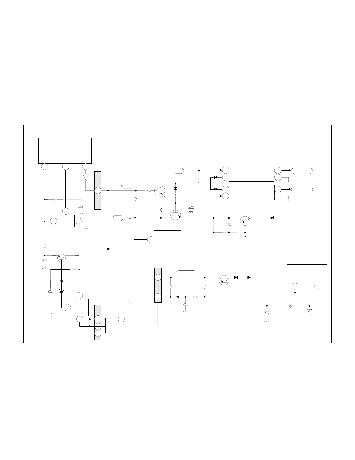
45
CIRCUIT DESCRIPTION
Off
Power On/Off
ZP-94/95 SERIES "POWER ON & OFF" DIAGRAM
I001
Microprocessor
53
PQS1
8
R958
D946
To Gate of Q914
(Shutdown SCR )
R959
6 Shutdown
Inputs,
Active Low
Power
On/Off
+28V
C948
SW+5V
Sub Power PWB
Signal PWB
RP36
CP44
HVcc
C964
Power/Deflection PWB
I701
H Drive IC
15
8
Def.B+
Hoz. Out
Signal Sub PWB
C544
2.5V
I907
SW+5V
Reg IC
5
1
I908
SW+12V
Reg IC
1
5
2
2
3
3
VDD
5V
L004
Q026
R029
D034
1
C074
STBY+5V
3.3V
3.9V
61
54
Reset
I006
Reset
2
3
1
SBY11V
3.3V
3.3V
C032
R053
I905
STY+7V
2
D035
Q002
I008
STBY
+5V
1
3
2
SYB
+7V
PQS2
D928
D948
SW+12V
R949
R950
+28V
D947
PQD2
1
DP21
RP38
RP37
QP04
DP35
DP36
3
L701
I906
STY+11V
2
2
3
Q909
Q908
R957
D945
Q903
R951
Off On
On
C949
C075

CIRCUIT DESCRIPTION
ZP94/95 MICROPROCESSOR DESCRIPTION EXPLANATION:
The ZP94/95 Microprocessor is a Duel In-Line 64 pin chip. The Microprocessor is responsible for many
different operations related to the control of the Projection Television. Some of these controls are automatic
and some require customer intervention, either by the Remote control or front panel keys and/or by the
customers menu. When power is first applied, the Microprocessor receives its B+ voltage. This Microprocessor utilizes a 3.3V power supply instead of the usual 5V as in past chassis. As the 3.3V is rising, the
Reset IC (I006) holds the reset pin (54) low long enough for the main B+ to stabilize. After stabilization, the
Reset IC brings pin (54) high. During the Reset condition, the Microprocessor is initiated into is start up
state. At the same time this is happening, the Microprocessor Oscillator is generating the Microprocessors
internal clock. The Crystal responsible for this is X001 (4Mhz) connected to pins (52 and 53). When
trouble shooting a Microprocessor for problems, its very important to remember the sequence described
above. Always examine the process before looking for any other problem area.
The order is;
1. Vcc Applies. Generated from the Always Voltage (STY+7V I905) on the Sub Power Supply then
through a 3.3V regulator (STBY +5V I008 on the Signal PWB).
2. Ground is available. Look for open traces, etc.
3. The Reset circuit is working (I006). It should hold the Reset pin on the Microprocessor low until main
Vcc becomes stabled.
4. The Oscillator is running. Be careful here because a low resistance probe will kill the Oscillator or give a
false reading.
After checking for the preliminary functionality of the circuits described above, then check for active clock
pulses leaving data port pins. (See the Data Communications Circuit Diagram for details). If some other IC
is grounding the data or clock pins, the Microprocessor will not work. This usually requires a pull-up
resistor. If no pull-up resistor is noted in the schematic, then the responsibility for pull-up lies within the
Microprocessor. Unloading the pin is a good way to investigate for pull-up. When Remote Control, Front
Keys or some internal process enters a command, the Microprocessor runs a set of predetermined routines.
These routines are hard programmed into the Microprocessor RAM and are unchangeable. There are
routine instructions that can be modified by either the customer or the Servicer and involve pre-programmed
routines and variables entered by the customer or technician. These would include such things as changing
the channel, audio set-ups, on/off timer, auto-link, etc...
CONTROL OF THE PROJECTION TELEVISION:
Receiving Inferred Remote Control Commands
Receiving Key Input Commands
Controlling the On and Off state of the High Voltage Power Supply
Interaction between the Customers Menu and Chassis controls
Outputting of On Screen Display information
Interaction between the Service Menu and Chassis I 2 C Data Bus controls
Automatically Scanning the Tuners searching for Active Channels when requested by the Customer from
the Menu
Automatically Controlling the Tuners when Channels are changed for the Main and PinP Tuners
Automatically Controlling the Video Processor (Rainforest IC) when directed by the Customer
Controlling the Audio Circuits when directed by the Customer.
Controlling Switching between Tuner (Main), AVX 1, 2, 3 and 4, Component 1, 2, and Tuner 2 (AUX) or
In From Converter.
The following section will explain the controls listed above.
46

EEPROM
DAC 1
DAC 2
Rear Audio
Control
CIRCUIT DESCRIPTION
ZP-94/95 SYSTEM CONTROL PORT DESCRIPTION
I001
VDD (3.3V)
Dimmer
POO
VSS (Gnd)
DSP Reset
AC In
OSD X1
OSD Xo
OSD B
OSD R
OSD G
OSD B
OSD Blk
Powe r O n/Off
VRef
B+Fail
Half Tone
SCL
I002
SDA
SCL
I003
SDA
SCL
I004
SDA
SDA
IS11
SCL
Main CCD
Sub CCD
OSC In
OSC Out
VSS (Gnd)
IRIn
VRefHS
CLH
Ft. Panel Control Keys
61
4
41
29
19
23
48
47
39
37
38
39
51
53
36
9
40
3
SCL1
2
SDA1
57
SDA3
SCL3
56
28
30
62
63
64
1
27
26
AD
5
KeyIn
FE Enable1
Main/Sub AFC
FE Enable2
FC Enable
DSP Err Mute
DSP Sck
DSPRST
DSP Busy
SO Select
AV D D 3.3V
Sub FV Det
Main FV Det
G+Reset
Key In
Clock
Data
DSP SI
DSPSS
DSP S0
SCL2
SDA2
Reset
IRef
BVCOI
Test
CLL
Comp
VMute
VSync
44
6
43
7
20
21
46
17
18
16
15
19
13
12
60
59
50
54
35
42
33
52
32
11
10
34
8
45
55
I014
Level
Shift
N/C
CLOCK
DATA
ENABLE
AFC
DATA
CLOCK
ENABLE
AFC
Clock
Data
Enable
DSP SI
DSP Err
DSP Sck
DSPSS
DSPRST
SCL
SDA
SCL
SDA
SCL
SDA
SCL
SDA
SCL
SDA
SCL
SDA
SCL
SDA
SCL
SDA
U204
I701
IX01
IS03
IS05
IS05
IS10
IS08
IS01
U201
MAIN
TUNER
U202
PinP
TUNER
U205
Flex Conv & PinP
Unit
Audio DSP
AC3/ProLogic
3D/YC
Comb Filter
Deflection
Rainforest
IC
Front Audio
Control
Front EQ
Cent EQ
Cent/L F E/PinP
Audio Control
DAC3
47

CIRCUIT DESCRIPTION
Pin ID Function Active
1 IRIN Rec ei ves Remot e Control Inferred pulses . Data
2 S DA1 Serial Dat a S ent and Rec ei ved from the E E PROM, A/ V Select or, DAC1, DA C2.
Func tion of I2C.
3 SCL1 Serial Cl ock S ync hroniz ation Sent to t he EEP RO M , A/V Select or, DA C1,
DAC2. Function of I2C.
4 Dim m er Recei ves DC voltage generated from t h e P hoto Rec ei ver on the Front Panel
monitoring Room Light. For AI
5 AD Key In Receives Level Shi ft ed DC voltage from Front P anel Key press es. DC
6 Main/Sub
AFC
7 K ey In W hen the P ower s wi tc h i s pres sed, Cl ock data from pin 21 i s rout ed through
8 Not Us ed Not Used N/A
9 Not Us ed Not Used N/A
10 Main FV
Det
11 Sub F V Det Receives Compos i te 2 V S ync from I016 pi n 4 for OS D P osi t i on i ng. Sync
12 DSP B u s y Receives t he B usy com m and from t h e Di gi t a l S urround Proc ess or on the
13 DSP SO Control comm and t o the DSP Unit for c on t rol l ing Modes. Data
14 DSP Di r Recei ves Digi t al Surround Proc ess or E rror i nforma t ion from t he DS P un i t on the
15 DSP SS Control c o m m and to t he DS P Uni t for controll i ng Mo des . Dat a
16 DSP SCK Di gital Surround Proc e ss or Cl ock. Data
17 DSP S1 Control c o m m and to t he DS P Uni t for cont rolli ng M odes. Data
18 DSP E RR
Mute
19 DSP Reset Res ets the DSP m odu l e on the Surroun d P WB DC High
20 Clock S ent to t he Level Shi ft I014 t hen to bot h Tuners and the Fl ex Converter as a
21 Data Sent to t he Level Shi ft I014 t hen to bot h Tuners and t h e F l ex Converter t o
22 Comp 1/ 2
FH Det
23 AC In Recei ves Timi ng pul ses for advanci ng t he Cl ock . Rec ei ved from the Sm it t Amp
24 Main/Sub
SD Det
25 VDD Stb y +3.3V generated by 00 29. M ai n Mic roproces sor B+. DC
26 CHL Clamp level High DC
27 VRefFHS Use as a reference s i gnal wi t h i n the Mi croproc ess or Hi gh F requenci es . DC
28 CV BS0 Com posite S ync used for Clos ed Caption Detec t i o n for t he M ai n Tuner. Sy nc
29 VSS Ground N/A
30 CVB S 1 Not Us ed. Composite Sy nc used for Closed Caption Detec tion for the PinP
31 VREFLS Reference S i g nal used wit h i n the Mi croproc ess or Low Fr equencie s . N/A
32 CLL Internal function of t he M ic roprocessor. N/A
Recei ves t he M ai n Tuner AF C or S ub A F C DC V ol t a ge swit ched by I005. Used
during c h annel change.
Q014 bac k t o this pin. Power i s t oggl ed On or O ff.
Recei ves Composite 1 V S ync from I015 pi n 4 for OS D P ositioni ng . Sy nc
Surround P WB .
Surround P WB .
Mut es A udi o when a DS P Di r i nput is det ect ed. (DSP E rror). DC High
ti m i ng si gnal . Al so s e e pi n 7.
control each uni t .
Ei ther Component One or Two Horizontal Input from I005 through Q046. Us e d
for OSD Display. And Auto Link
Q008 and Q009
St a t ion Detect i on. Us ed duri ng Aut o P rogram m i ng and when channels are
change d t o open A F C Loop. Swi tc hed by I005.
Tuner.
Data
Data
DC
DC
Data
DC
Data
Data
Data
DC
60Hz.
Sync
N/A
48

CIRCUIT DESCRIPTION
Pin ID Function Ac tive
33 AV DD Stby +3.3V generated by 0029. DC
34 COMP Internal funct ion of the Mi croprocess or. DC
35 IREF Internal function of the Microprocessor. DC
36 VREF Internal function of t he Microprocessor. DC
37 OSD R Outputs Red c haracters for the S ervice Menu. Dat a
38 OSD G Outputs Green characters for the S ervice Menu. Data
39 OSD B Output s Blue characters for the S ervice Menu. Data
40 HALF
TONE
41 PDO Internal func ti on of t he Microprocessor. DC
42 BVC0I Internal func ti on of t he Microprocessor. DC
43 FE
ENABLE 2
44 FE
ENABLE 1
45 V.MUTE Mutes A udio and Video through Q008 and Q010 to Sub Video and Surround
46 FC
ENABLE
47 OSD X0 Reference F requency for OSD. Determi nes t he OS D S i ze. Data
48 OSD X1 Reference F requency for OSD. Determi nes t he OS D S i ze. Data
49 H SY NC Receives Horizontal Blanking pul ses 3.3Vp/p for OSD posi ti oni ng. Generated
50 SD
SELECT
51 OSD BLK Outputs a pulse slight wider and in t ime with the OS D c haract ers t o clean up
52 TEST Use by the factory for i nternal test of the Microprocessor and to place i n a
53 Power
ON/OFF
54 RESET Low when Power first applied t hen rises t o a hi gh of 3.3V. Received from I006.
55 VSY NC Receives Vert ical Bl anking pul ses 3.3Vp/p for OSD posi tioning. Generated from
56 P BLK Sent to the Rainforest IC IX01. Used to Mute t he Video during Channel change,
57 SDA3 Serial Data Sent to t he Rear Audio Output IC IS11 on Surround PWB. Cont rols
58 SCL3 S erial Clock Sent to t he Rear Audi o Output IC IS11 on Surround PWB. Used for
59 SDA2 Serial Data Sent to U204, I701, IX01, IS 03, IS05, IS10, IS08, IS01, I201 and
60 SCL2 S erial Clock Sent to U204, I701, IX01, IS03, IS05, IS 10, IS08, IS 01, I201 and
61 VDD S tby +3. 3V generated by 0029. Main Microprocessor B+. DC
62 OSC In O SC In (4M Hz) Dat a
Controls t he Translucency of t he M ain Menu Background. Low = Clear, M id =
Transparent, Hi = Gray.
Front End Enable. Enables the reception of data from the Microproc essor by t he
Pi nP Tuner.
Front End Enable. Enables the reception of data from the Microproc essor by t he
Main Tuner.
PWB during channel change. High = Mute
Flex Converter Enabl e Line. A llows the Fl ex Converter t o receive commands
from the M ic roprocessor.
from H Blk through Q006
Sent through Q030 to I015 for setting the internal select ion switches. Hi = M ain,
Lo = S ub
video where charac ter will be displayed.
specifi c s et of cri teria.
This out put goes high when the Power Butt on i s pres sed for ON and Low for Off. DC
Reset s the Mic roproces sor.
V B lk through Q005
Child Lock, AVX selected with no input. Hi = Mute
Vol ume, Bass , Treble, and B al . Function of I2C.
Timing of Data. F unct ion of I2C.
I403. Function of I2C.
I403. Function of I2C.
Data
Data
Data
DC
Data
H Blk
DC
Data
DC
DC
Data
DC
Data
Data
Data
Data
49

CIRCUIT DESCRIPTION
Receiving Inferred Remote Control Commands:
Whenever the Customer utilizes the Infer-red Remote, the IR receiver will detect these 38Khz inferred pulse
train and amplify them. These pulses are delivered to the Microprocessor at Pin (1). The Microprocessor
decodes this data train and sets off the internal routine related to the command.
There is a time when the Microprocessor ignores the remote commands and that is when the Digital Convergence Unit, (DCU here after) is in operation. The Microprocessor receives a BUSY notification that the
DCU is in operation and simply doesnt respond to remote commands. (See the Digital Convergence
Interconnect Diagram and explanation for complete details.) The BUSY signal is generated from the DCU
at pin (10). Then out pin (1) of the PSD1 connector to pin (10) of I004 DAC2. I004 sends the information
via SCL1 and SDA1 lines from Pin (14 and 15) to the Microprocessor pins (2 and 3).
Receiving Key Input Commands:
The front panel function keys are detected by the Microprocessor via R2 ladder style circuit. In other
words, inside the microprocessor is a group of comparators. The function keys are strung together and each
one has a different resistor value to ground. When the key is pressed, the comparators detect the change is
resistance to ground at pin (20) Clock and convert the related DC value into data the Microprocessor can
understand.
The following shows the resistor value to ground from pin (20) of the Microprocessor, though pin (7) of the
PFS connector to the individual keys.
Channel Up = ground
Channel Down = 1K
Volume Up = 1K + 1.5K or 2.5K
Volume Down = 1K + 1.5K + 2.7K or 5.2K
AVX = 1K + 1.5K + 2.7K + 4.7K or 9.9K
Menu = 1K + 1.5K + 2.7K + 4.7K + 10+ or 19.9K
Controlling the On and Off state of the High Voltage Power Supply.
The Power On/Off function switch has STBY+3.3V applied for the Sub Power Supply, via pin (8) of the
PFS connector through a 1K resistor. The output of the Power On/Off switch is sent through pin (6) of the
PFS to Q014. Q014 is turned on at this time and connected to its Emitter is the Data from the Microprocessor pin (21). The Data is routed from Q014s Collector to Key in pin (10) of the Microprocessor. When
the Microprocessor receives this data at pin (10), it knows to turn on or off the television. This function is
performed by and output from pin (53), which controls Q002. This output from this pin is High when the set
is On and Low when the set is Off.
(For more details related to Power On/Off, see the Power On & Off Circuit Diagram Explanation and
Diagram).
Interaction between the Customers Menu and Chassis controls.
When the Customer accesses the Main Menu, selections can be made by scrolling up and down or left to
right. Each item selected will activate a set of instructions within the Microprocessor and determine the
output state of the related pins.
Outputting On Screen Display information
When its necessary, the Microprocessor generates 1uSec pulses from pins (37 Red, 38 Green and 39
Blue) that are sent to the Rainforest IC (IX01) pins (37 Blue, 38 Green and 39 Red) as OSD signals. When
the OSD signals are high, they turn on the output of the Red or Green or Blue amps inside the Rainforest IC
and output a pulse to the CRTs to generate that particular character in the particular color.
50

51
CIRCUIT DESCRIPTION
DSPSS
DSPSCK
DSPERR Mute
DSPI
DSPRST
ZP94/95 CHASSIS MICROPROCESSOR DATA COMM UNICATIONS CIRCUIT DIAGRAM
IOO1
PSZ2
IX01
Rainforest
RGB
Processor
2H Video PWB
60
59
SCL2
SDA2
PSD2
Sweep Control
Surround PWB
Clock
Data
U205
FLEX
&
PinP
PFC1
Enable
Clock
Data
FCENAble
1217
16
SCL2
SDA2
SDA2
26
27
SCL2
2
1
I201
Main Video
Chroma
33
34 SDA2
SCL2
SDA2
SCL2
U204
3DY/C
PYC1
2
3
I014
3.3V -> 5V
Level Shift
2
3
4
5
6
7
18
17
16
15
14
13
20
21
46
15
16
18
8
9
12
11
17
19
DSPSS
DSPSCK
DSPERR Mute
DSPI
DSPRST
PSU2
5
2
6
3
1
PSU1
2
1
IS03
Front
Audio
Control
SCL2
SDA
2
IS08
Center/LFE/
PinP
Audio Control
IS10
Center
Equalizer
IS05
Front
Equalizer
SCL2
SDA2
SCL2
SDA2
IS01
DAC3
SCL2
SDA2
I403
Sub
Video
Chroma
PST1
Deflection PWB
Signal PWB
I701
9
12
8
11
13
DSP
Unit
HC4051
PMU1
5
6
I401
A/V Select
SCL1
34
33
SDA
1
FCEN
SCL2
SDA2
SCL2
SDA2
10
11
12
4
5
4
5
17
16
17
16
14
15
3
2
SCL1
SDA1
IOO2
EEPROM
5
6
SDA1
SCL1
I004
DAC2
SDA1
SCL1
5
65
6
SDA1
SCL1
I003
DAC1
SCL3
SDA3
58
57
SCL3
IS11
Rear
Audio Control
SDA3
Terminal PWB
345
4
DSPSS
DSPSCK
DSPERR Mute
DSPI
DSPRST
FEENABLE2
43
17
U202
Tuner 2
Pinp
16
Clock
Data
15
Enable
6
Enable
U201
Tuner 1
Main
FEENABLE1
44
5
Clock
Data
4
33
34 SDA2
SCL2
2
1

CIRCUIT DESCRIPTION
Interaction between the Service Menu and Chassis I 2 C Data Bus controls
When it becomes necessary for the Service Technician to adjust the set, the Service Menu must be entered.
This is accomplished with the TV turned off, then by pressing and holding the INPUT Key and then the
POWER SWITCH. The Adjustment Menu will be displayed at this time. With the Service Menu activated,
the Technician moves up and down to the desired adjustment using the Remote control or front panel Up or
Down cursor keys. To make the adjustment, the Technician uses the Remote control or front panel Left and
Right cursor keys to change the data values for the particular adjustment. The Microprocessor controls the
individual IC related to the adjustment using I2C technology. I2C technology allows the Microprocessor to
control and IC using only two pins, (SCL and SDA). The following pins on the Microprocessor and the ICs
that it controls are described in the following table.
PINS CONTROLLED ICs
2 SDA1 and 3 SCL1 I401 AV Selector, I002 EEPROM, I003 DAC 1, I004 DAC 2
59 SDA2 and 60 SCL2 U204 3D/YC, I701 Deflection Drive, IX01 Rainforest, IS03 Front
Audio Control, IS05 Front EQ, IS10 Center EQ, IS08 Center/
LFE/PinP Audio Control, IS01 DAC3, I201 1H Main Video, and
I403 H Sub Video.
57 SDA3 and 58 SCL3 IS11 Rear Audio Control.
Automatically Scanning the Tuners searching for Active Channels when requested by the Customer from the Menu.
When the Projection is first installed, the active channels must be scanned and memorized in the Channel
Scan List. This list is actually stored within the EEPROM and the Microprocessor uses the information to
Scan up or down. Held within the Microprocessor is the Initial FCC Lookup table. This table gives information related to all the channels frequency, band, and channel number. The frequency is actually a given
value for the Phase Lock Loop circuit within the tuner. Then band is data to tell the band selection circuit in
the tuner where the particular channel is located and the channel number is given to the microprocessor to
indicate what OSD outputs to pro-duce. When the set is first opened, its in what is called Factory Reset
Condition. For the Tuner, this means that the signal source is AIR, and channels 2 through 13 are in the
channel scan list. Before the customer runs Auto Program, they must set the signal source to the type they
are using, Air, Cable 1 or Cable 2. After the source is set, the customer then proceeds with Auto Programming. When Auto Programming is initiated, the Microprocessor has a specific program to run. This program
starts by placing the tuner in the lowest channel in the lowest band. That would normally be channel 2. Then
the program instructs the Microprocessor to look for Sync. To do this, the Microprocessor actually need
Horizontal Blanking (H.Blk) at pin (49) which is labeled H.Sync and Video Sync (24) labeled Main/Sub SD
Det. Horizontal Blanking is use as a gate pulse for the coincidence detector. Within the coincidence detector
there is a circuit that monitors the timing of the Sync pulse in relationship to (H.BLK). If the signal being
checked is not in time with (H.Blk) the signal is ignored. However, if the signal being monitored is in coincidence with (H.Blk), the signal is deemed to be true Video Sync and that particular channel is stored as an
active channel in the EEPROM Scan List. Then the Microprocessor sends information to the tuner to move
up one channel and the whole process begins again. This is repeated until every channel is checked. After
completion of the scan, the microprocessor retrieves information from the EEPROM concerning the first
channel in the lowest band that appears in the scan list and directs the tuner to tune to that channel.
52

CIRCUIT DESCRIPTION
Automatically Controlling the Tuners when Channels are changed.
MAIN TUNER:
When channels are changed, the Microprocessor runs another routine. This routine detects the command if
the Remote Control or the Front keys input it. Whether its Scan Up/Down or direct access, and begins to
control the Tuner. First, the Microprocessor output a Mute command to blank the video, then data is sent to
the tuner to move it to the desired channel. After that, the Microprocessor again checks the coincidence
detector for active sync. If active sync is detected, the Microprocessor opens what is called the AFC Loop.
The AFC Loops comprises two cycles trying to lock the tuner to the specific IF frequency of 45.5 Mhz. A
DC voltage is sent from either the Main Tuner U201 pin (10) or the PinP Tuner U202 pin (21) back to the
Microprocessor pin (6). This DC voltage indicates the error between the IF detected and the IF frequency
reference. This error voltage tells the Microprocessor to do one of two things. First, if the error is large, the
Microprocessor changes the Programmable Dividers division rate to a larger or smaller degree to get
closer to the actual IF frequency desired. Second, move the Pulse Swallow division rate to either 1/32 or 1/
33. The Pulse Swallow tuning circuit is a second divider that is on the output from the Prescaler. The main
Prescaler takes the very high frequency output from the tuners mixer circuit which is produced when the
tuners main oscillator is beat against the incoming RF frequency. The Programmable Divider is instructed by
the Microprocessor exactly what division rate to apply to the Beat Frequency generating the IF frequency.
The IF frequency is then sent through the Pulse Swallow circuit which again divides the IF frequency at a
much smaller rate. This allows the IF output frequency to become much more finite and can correct for
much smaller errors between the Phase comparators reference frequency. The error voltage is routed back
to the main internal Oscillator in the front end to correct for Tuning errors.
(See the Microprocessor Data Communications Circuit Diagram Explanation for Details related to Data
Communication for controlling the Main Tuner).
Automatically Controlling the Tuners when Channels are changed.
PinP TUNER:
As far as the internal function of the PinP Tuner, it is the same as the Main Tuner. When the customer
presses the PinP button on the Remote Control, the Microprocessor outputs Clock, Data and Enable
controls to the Flex Converter. The Flex Converter also has the PinP circuit inside. The Clock, Data and
Enable pins on the Microprocessor are pins (20 Clock, 21 Data and 46 FCENABLE) These are routed to
the Level Shift IC, I014 pins (2, 3 and 4). They are output on pins (18, 17 and 16) to the Flex Converter
U205 connector PFC1 and input on pins (10, 11 and 12). The Flex Converters PinP unit is then switched
on and insertion is made into the regular Main Video line. This process controls the position of the PinP
window, the PinP window itself and other different display conditions. When SWAP is pressed on the
remote control, the channel or input that the PinP tuner was on, now becomes the Main Videos source and
the channel or input that the Main signal was on, now becomes the PinP source.
Automatically Controlling the Video Processor (Rainforest IC) when directed by the Customer.
The Rainforest IC has many enhancement circuits built in. These would include the Black Peak Expansion
circuit, the Dynamic Noise Reduction circuit, Time Compression and of course Sharpness, Black Level and
Contrast adjustments as well.
Black Peak Expansion Circuit:
This circuit is utilized to increase the contrast ratio. The standard video signal is 1-Volt Peak to Peak; the
actual video (Y) content is 730mVp/p. The Standard video signal is divided into units called IRE. The units
are equal to 140 total for the 1Vpp signal. Sync occupies 40IRE, which are negative and the Luminance
represents 100 IRE units. Each unit represents 7.1428mVp/p of information. The Black Peak Expansion
53

CIRCUIT DESCRIPTION
circuit monitors the 1/2 way point of luminance, (50 IRE or 357mV) and pulls the signal towards pure black
or the 7.5 IRE level. This increases the distance from Black Peak to White Peak, which is contrast.
Dynamic Noise Reduction Circuit:
This circuit again monitors the area from 50 IRE down and subtracts noise. This circuit is dynamic meaning
that it characteristics change. In other words, the subtraction process is greater near black level that it is
near 50 IRE. The subtraction is 6dB at maximum, meaning that there would be some frequency loss near
black, but the noise, which is seen as white speckles, would be reduced.
Time Compression Circuit:
Any time an analog signal is passed through a capacitor, its high frequencies are reduced. To replace these
high frequencies, Zenith uses Time Compression. This circuit is on the order of Aperture Compensation,
however it differs in the fact that it uses 5 delay lines. The actual signal should look like Figure 2. Figure 3,
however after passing through a capacitive circuit, it looks like Figure 4. After Time Compression takes
place, the beginning rise is advanced. Just before white peak, the signal is delayed. Just before the signal
falls the signal is advanced and just before the signal reaches black peak the signal is delayed. This causes
the signal to appear more like the actual signal and thus restores the high frequencies lost through capacitance.
Sharpness:
During the Time Compression process, switching pulses that are detected at the transition point, (A transition is the point at which the luminance signal goes for black to white or white to black) are used in the
sharpness circuit. This signal is the routed through a sort of variable resistor and according to how much
sharpness the customer has selected, determines how much of the transition signal is added to the original
signal. The greater the sharpness setting, the greater the transition signal added.
Controlling the Audio Circuits when directed by the Customer.
The customer has control over how the set accesses audio information for all of its inputs. The tuner for
example is an integrated type. This not only means that held within the Main Tuner is all the necessary
components for Reception and Video detection. It also has a built in audio and MTS decoder. The Main
Tuner outputs Left Total and Right Total signals. (Left Total and Right Total means that the encoding for
Pro-Logic is held within the individual signal.) The customer can select first, how the Tuner decodes its
audio. Stereo, Mono, or SAP can be selected. The Main Tuner must tell the Microprocessor what signal it
is receiving. The Main Tuner has a ST LED output at pin (19), which tells the Microprocessor it is receiving
MTS Stereo and a SAP LED output at pin (20), which tells the Microprocessor it, is receiving Second
Audio Program. How these are selected by the consumer via the Main Menu determines the output from
the Microprocessor.
ST LED is routed from the Main Tuner at pin (19), through Q204, to the DAC1 I003 pin (10). The DAC1
outputs Clock and Data via pins 15 SCL1 and 14 SDA1 signals to the Microprocessor input on pin 3
SCL1 and pin 2 SDA2. The Microprocessor knows how to switch the tuner decoder circuit by making
judgment upon these inputs. Then the Microprocessor can us Clock, Data and Enable lines to control the
Tuner.
SAP LED is routed from the Main Tuner at pin (20), through Q203, to the DAC1 I003 pin (9). The DAC1
outputs Clock and Data via pins 15 SCL1 and 14 SDA1 signals to the Microprocessor input on pin 3
SCL1 and pin 2 SDA2. The Microprocessor knows how to switch the tuner decoder circuit by making
54

CIRCUIT DESCRIPTION
judgment upon these inputs. Then the Microprocessor can us Clock, Data and Enable lines to control the
Tuner. Clock, Data and Enable lines for the Main Tuner are output from the Microprocessor at pins (20, 21
and 44) respectively. Pin (44) FEENABLE1 goes directly to the Main Tuner at pin (6), where as the Clock
and Data lines must be routed through the Level Shift IC I014 to be brought up to 5V. Clock and Data
arrive at I014 at pin 2 and pin 3 and are output at pin18 and pin17. They arrive at the Main Tuner at pins (4
and 5). The PinP Tuner doesnt have MTS capability. It only output mono audio, so no switching takes
place for the PinP Tuner U202 audio circuit. The only difference for the PinP tuner control lines is related to
the PinP Enable line. This is output from the Microprocessor pin (43 FEENABLE2) to the PinP Tuner at pin
(17). Clock and Data are the same as for the Main Tuner.
Controlling Switching between Tuner (Main), AVX 1, 2, 3 and 4, Component 1, and 2, and Tuner 2
(AUX) or In From Converter.
The Remote Control or the Front Panel switches can select the different inputs. This is accomplished by the
INPUT button. Each time the Input button is pressed, the different inputs are sequentially selected. The
sequential order is, Main Tuner, AVX 1, AVX 2, AVX 3, AVX 4, 2nd Antenna and back to Main Tuner. In
addition, if there are S-Inputs on AVX1, 2 or 4, an internal mechanical switch inside the S-Jack tells the
Microprocessor an S-Jack is inserted. Then when that particular input is selected, it automatically selects S
as its source. The same thing holds true for Component inputs. The set should never have Component
inputs and S-Jack inserted at the same time. This will cause a black and white picture will be displayed.
PAGE 02-11
Use this explanation in conjunction with the Microprocessor Data Communications circuit diagram.
The Microprocessor must keep in communication with the Chassis to maintain control over the individual
circuits. Some of the circuits must return information as well so the Microprocessor will know how to
respond to different request. The Microprocessor uses a combination of I 2 C Bus communication and the
Standard Data, Clock and Load lines for control. The I 2 C communication scheme only requires 2 lines for
control. These lines are called SDA and SCL. System Data and System Clock respectively. The Microprocessor also requires the use of what are called Fan Out IC or DACs, (Digital to Analog Converters). This
allows the Microprocessor to us only two lines to control many different circuits. In addition, because this
Microprocessor operates at the new 3.3Vdc voltage, it requires a Level Shift IC to bring up the DC level of
the control lines to make it compatible with the connected ICs. The Microprocessor communicates with the
following ICs:
ON THE SIGNAL PWB:
Main Tuner U201
PinP Tuner U202
EEPROM I002
Flex Converter U205
DAC1 I003
DAC2 I004
Level Shift I014
3D Y/C U204
Main Video Chroma I201
55

CIRCUIT DESCRIPTION
ON THE TERMINAL PWB:
A/V Selector I401
Sub Video Chroma I403
ON THE DEFLECTION PWB:
Sweep Control I701
ON THE SUB VIDEO PWB (2H VIDEO):
Rainforest IX01
ON THE SURROUND PWB:
Front Audio Control IS03
Center/LFT/PinP Audio Control IS08
Surround Board DAC3 IS01
Front Equalizer IS05
Center Equalizer IS10
Rear Audio Control IS11
Audio DSP (Digital Signal Processor) DSP Unit HC4051
The following explanation will deal with the communication paths used between the Microprocessor and the
respected ICs.
ON THE SIGNAL PWB:
Main Tuner U201
The Microprocessor controls the Main Tuner by Clock, Data and Enable lines. Clock, Data and Enable
lines for the Main Tuner are output from the Microprocessor at pins (20 Clock, 21 Data and 44
FEENABLE1) respectively. Pin (44) FEENABLE1 goes directly to the Main Tuner at pin (6), where as the
Clock and Data lines must be routed through the Level Shift IC I014 to be brought up to 5V. Clock and
Data from the Microprocessor arrive at I014 (Level Shift) at pins 2 and pin 3 and are output at pin18 and
pin17. They arrive at the Main Tuner at pins (4 and 5).
PinP Tuner U202
The only difference for the PinP tuner control lines is related to the PinP Enable line. This is output from the
Microprocessor pin 43 (FEENABLE2) to the PinP Tuner at pin 17. Clock and Data are the same as for the
Main Tuner.
EEPROM I002
The EEPROM is ROM for many different functions of the Microprocessor. Channel Scan or Memory List,
Customer set-ups for Video, Audio, Surround etc are memorized as well. In addition, some of the
Microprocessors internal sub routines have variables that are stored in the EEPROM, such as the window
for Closed Caption detection. Data and Clock lines are SDA1 from pin (2) of the Microprocessor to pin
(5) of the EEPROM and SCL2 from pin (3) of the Microprocessor to pin (6) of the EEPROM. Data
travels in both directions on the Data line.
56

CIRCUIT DESCRIPTION
Flex Converter U205
The projection television is capable of two different horizontal frequencies. 31.75Khz for everything except
HD and 33.75Khz for HD. (High Definition). The Flex Converter is responsible for receiving any video
input and converting it to the related output. This output is controlled by the input sync and by the
customers menu. The set up can be 4X3 or 16X9 sometimes called letterbox. The Flex Converter can take
any NTSC, S-In, Component in NTSC, Progressive or Interlaced, and 480I, 720P, 1080I signal. Control
for the Flex Converter is Clock, Data and Enable lines. Clock, Data and Enable lines for the Flex Converter
are output from the Microprocessor at pins (20 Clock, 21 Data and 46 FCENABLE). FCENABLE Clock
and Data lines must be routed through the Level Shift IC I014 to be brought up to 5V. They arrive at I014
at pins (2 Clock, 3 Data and 4 FCENABLE) and are output at pins (18, 17 and 16) respectively. DAC1
I003 This Digital to Analog converter acts as an extension of the Microprocessor sometimes called an
Expansion IC. The purpose of this IC is to reduce the number of pins, (fan out) of the Main Microprocessor
I001. The Main Microprocessor sends Clock and Data via I2C bus to the DAC1 IC. The output from the
Microprocessor is pin (2 SDA1 and 3 SCL1) which arrives at the DAC1 IC at pins (5 and 6) respectively.
The following is a list of the input and output pins on DAC1.
PIN FUNCTION
1. IR Det. The IR pulse from the Remote Control is monitored when Auto Link is set. (See
Auto Link in Index).
2. YN Det. Active Low. This pin monitors for active sync when Auto Link is set. (See Auto
Link in Index).
3. Blk Main Normal High, Blanking Low. Blanks Y-Cb/Cr into Flex Converter.
4. MTS Places the Main Tuner pin (21 mode) into MTS Stereo. If Tuner receiving MTS
signal. See pin 10.
5. F Mono Places the Main Tuner pin (22 mono) into forced Mono Mode.
6. Ant Switches the antenna block into Antenna A or Antenna B when selected.
7. Blk Sub Normal High, Blanking Low. Blanks PinP Sub Y-Cb/Cr on Terminal PWB before
going into Flex Converter.
8. Gnd Ground
9. SAP Det The Main Tuner outputs an SAP LED signal when SAP is detected. Active Low.
10. ST Det The Main Tuner outputs an ST LED signal when Stereo is detected. Active Low.
11. SAD0 Ground Not Used
12. SAD1 Ground Not Used
13. SAD2 Ground Not Used
14. SDA Data I 2 C communications between DAC1 and Microprocessor
15. SCL Clock I 2 C communications between DAC1 and Microprocessor
16. Vcc IC B+. (STBY +5V)
57

CIRCUIT DESCRIPTION
DAC2 I004
This Digital to Analog converter acts as an extension of the Microprocessor. Sometimes called an Expansion
IC. The purpose of this IC is to reduce the number of pins, (fan out) of the Main Microprocessor I001. The
Main Microprocessor sends Clock and Data via I2C bus to the DAC2 IC. The output from the Microprocessor is pin (2 SDA1 and 3 SCL1) which arrives at the DAC2 IC at pins (5 and 6) respectively.
The following is a list of the input and output pins on DAC2.
PIN FUNCTION
1. YUV Det1 Detects activity on Component Input number 1.
2. YUV Det2 Detects activity on Component Input number 2.
3. FH Det Out 1 Test Point 1 (TP1).
4. Sel5 Controls IX02 on 2H PWB. Selects either Y Cb/Cr or Y IQ to com
pensate for Chroma Phase angle used in Auto Color.
5. F Mono Places the Main Tuner pin (22 mono) into forced Mono Mode.
6. FH Det Out 1 Test Point 2 (TP2).
7. 31/33 Notifies the DCU related to Horizontal Frequency. Either 31.75Khz
for everything but HD or 33.75Khz for HD. The DCU uses two sets
of memory. One for everything but HD and one for HD. This relates
to both Digital Convergence adjustment data and for Magic Focus
memory. Also notifies the Dynamic Focus Horizontal Parabolic
generator to compensate for phase distortion. Also, notifies I701
Horizontal Drive generation IC concerning the Horizontal operation
frequency.
8. Gnd Ground
9. CS Sel Not Used.
10. Busy Informs the Microprocessor that the DCU is in the Digital Conver
gence Adjustment Mode. The Micro. Ignores IR pulses.
11. SAD0 Ground Not Used
12. SAD1 Ground Not Used
13. SAD2 IC B+. (STBY +5V).
14. SDA Data I 2 C communications between DAC2 and Microprocessor
15. SCL Clock I 2 C communications between DAC2 and Microprocessor
16. Vcc IC B+. (STBY +5V).
Level Shift I014
The Microprocessor operates at 3.3Vdc. Most of the Circuits controlled by the Microprocessor operate at
5Vdc. The Level Shift IC steps up the DC voltage to accommodate.
3D Y/C U204
The 3D Y/C module is a Luminance/Chroma separator, as well as a 3D adder. Separation takes place
digitally inside the module. Using advanced separation technology, this module separates and doesnt
produce dot pattern interference or dot crawl. The 3D effect is a process of adding additional signals to the
Luminance and Chroma. These signals relate specifically to transitions. Transitions are the point where the
signal goes from dark to light or vice versa. The 3D adds a little more black before the transition goes to
white and a little more white just before it gets to white. It also adds a little more white just before it goes
58

CIRCUIT DESCRIPTION
dark and a little more dark just before it arrives. This gives the impression that the signal pops out of the
screen or a 3D effect. The Microprocessor communicates with the 3D Y/C module via I 2 C bus data and
clock. The communications ports are from the Microprocessor pins (59 SDA2 and 60 SCL2) to the 3D Y/
C PYC1 connector pins (2 and 3) respectively. The Microprocessor also is able to turn on and off circuits
within the 3D Y/C module determined by customer menu set-up.
Main Video Chroma I201
The Main Video Chroma IC processes the video and chroma from the 3D Y/C module for the main picture.
It converts video into Y and chroma into Cr/Cb (NTSC Only). Communication from the Microprocessor
via pins (59 SDA2 and 60 SCL2) to I201 pins (34 and 33) respectively.
ON THE TERMINAL PWB:
A/V Selector I401
The A/V Selector IC is responsible for selecting the input source for the Main Picture as well as the source
for the PinP or Sub picture. Communication from the Microprocessor via pins (2 SDA1 and 3 SCL1) to the
PST1 connector pins (5 and 6) respectively then to I401 pins (34 and 33) respectively.
Sub Video Chroma I403
The Sub Video Chroma IC processes the video and chroma for the Sub or PinP picture. It converts video
into Y and chroma into Cr/Cb (NTSC Only). Communication from the Microprocessor via pins (59 SDA2
and 60 SCL2) to connector PST1 pins (1 and 2) I403 pins (34 and 33) respectively.
ON THE DEFLECTION PWB:
Sweep Control I701
The Sweep Control IC is responsible for generating Horizontal Drive and Vertical Drive signals. The Microprocessor must tell the IC when certain things are done in the Service Menu. When Cut Off is performed,
the Vertical is collapsed. The Microprocessor tells I701 to stop producing Vertical Drive. At the same time,
I701 must stop the Spot Killer circuit from operating. This is accomplished by placing pin (24 DAC3) high
which activates QN07 which inhibits spot killer high. In addition, when H.Phase is adjusted, the Microprocessor controls the H. Drive signals phase in relationship to H.Blk, which is timed with video sync. This
gives the appearance that the horizontal centering is being moved. Communication from the Microprocessor
via pins (59 SDA2 and 60 SCL2) to the PSD2 connector pins (2 and 3) and then to I701 pins (16 and 17)
respectively.
ON THE SUB VIDEO PWB (2H VIDEO):
Rainforest IX01
The Video Processing IC (Rainforest) is responsible for controlling video/chroma processing before the
signal is made available to the CRTs. Some of the emphasis circuits are controlled by the customers menu.
As well as some of them being controlled by AI, (Artificial Intelligence). Communication from the Microprocessor via pins (59 SDA2 and 60 SCL2) to the PSZ2 connector pins (1 and 2) and then to IX01 pins (27
and 26) respectively.
59

CIRCUIT DESCRIPTION
ON THE SURROUND PWB:
Surround Board DAC3 IS01
This Digital to Analog converter acts as an extension of the Microprocessor. Sometimes called an Expansion
IC. The purpose of this IC is to reduce the number of pins, (fan out) of the Main Microprocessor I001. The
Main Microprocessor sends Clock and Data via I 2 C bus to the DAC3 IC. The output from the Microprocessor is pins (59 SDA2 and 60 SCL2) then through the connector PSU1 pins (2 and 1) which arrives
at the DAC3 IC at pins (14 and 15) respectively.
The following is a list of the input and output pins on DAC3.
PIN FUNCTION
1. SW Sel 1 Turns on/off QS01 which either adds or doesnt add Sub Woofer to Front L and
Front R for 3 way audio set up.
2. DSP CSI Digital Surround Module signal. If the Coax Audio input is noisy, the DSP tells
DAC3 to 2X invert the signal.
3. Opti/Coax Sel Controls IS17. Determines if the signal is 2X inverted due to noise.
4. RSPOFF Turns off the Rear Speaker outputs. Controlled by the customers menu.
5. CSPOFF Turns off the Center Speaker outputs. Controlled by the customers menu.
6. FSPOFF Turns off the internal Front Speaker outputs. Controlled by the customers menu.
7. SWSEL 2 Controls QS25 to add Front Left and Right to Sub Woofer.
8. Gnd Ground
9. P. Vol. Perfect Volume On/Off controlled by the customers menu. Note, when in ProLogic mode, Perfect Volume is Off.
10. DSPREQ DSP Request Input.
11. SAD0 Ground Not Used
12. SAD1 Ground Not Used
13. SAD2 Ground Not Used
14. SDA2 Data I 2 C communications between DAC3 and Microprocessor
15. SCL2 Clock I 2 C communications between DAC3 and Microprocessor
16. Vcc IC B+. (STBY +5V)
Front Audio Control IS03
The Front Audio Control IC has the ability to adjust balance, treble, bass, volume and mute. This mute is
the one that is activated when the mute button is pressed on the remote control. Communication from the
Microprocessor via pins (59 SDA2 and 60 SCL2) then through the connector PSU1 pins (2 and 1) which
arrives at the IS03 at pins (4 and 5) respectively.
Center/LFE/PinP Audio Control IS08
This IC has the ability to adjust balance, treble, bass, volume and mute for the Center channel. This mute is
the one that is activated when the mute button is pressed on the remote control. It also adjusts the volume
for the PinP audio sent to the transmitter outputs as well as the volume for the Sub Woofer called LFE (Low
Frequency Effects). Communication from the Microprocessor via pins (59 SDA2 and 60 SCL2) then
through the connector PSU1 pins (2 and 1) which arrives at the IS08 at pins (4 and 5) respectively.
60

CIRCUIT DESCRIPTION
Front Equalizer IS05
The Front Audio can be frequency adjusted to suite the particular room environment. The individual frequency notches are adjusted via the customers menu. The following frequency notches are adjusted by this
IC. 60HZ,
250HZ, 1KHz, 3KHz, and 10KHz. Communication from the Microprocessor via pins (59 SDA2 and 60
SCL2) then through the connector PSU1 pins (2 and 1) which arrives at the IS05 at pins (17 and 16)
respectively.
Center Equalizer IS10
The Center Audio can be frequency adjusted to suite the particular room environment. The individual
frequency notches are adjusted via the customers menu. The following frequency notches are adjusted by
this IC. 60HZ, 250HZ, 1KHz, 3KHz, and 10KHz. Communication from the Microprocessor via pins (59
SDA2 and 60 SCL2) then through the connector PSU1 pins (2 and 1) which arrives at the IS05 at pins (17
and 16) respectively.
Rear Audio Control IS11
The Rear Audio Control IC has the ability to adjust balance, treble, bass, volume and mute. This mute is the
one that is activated when the mute button is pressed on the remote control. Communication from the
Microprocessor via pins (57 SDA3 and 58 SCL3) then through the connector PSU1 pins (4 and 3) which
arrives at the IS11 at pins (4 and 5) respectively.
Audio DSP (Digital Signal Processor) DSP Unit HC4051
The Digital Signal Processor is responsible for decoding Dolby Pro-Logic, AC-3 audio and selecting the
output of the audio determined by the customers menu. Such as Off, Matrix, Hall, etc Control for the
DSP is routed from the Microprocessor pins (15 DSPSS DSP Surround Sound Mode, 16 DSPSCK DSP
Clock, 17 DSPI DSP Mode 1, 18 DSPERR Mute DSP Error Mute, and 19 DSPRST DSP Re-set). Then
to the Level Shift, IC I014 pins (5, 6, 8, 7, and 9) respectively. These signals are then routed to the PSU2
connector pins (5, 2, 3, 6, and 1) respectively to the DSP module via the PMU1 connector pins (9, 12, 11,
8 and 13) respectively.
OSD Genaration
The Microprocessor is responsible for generating On Screen Display (OSD) related to the Main Menu,
Volume Control, Channel Number, Closed Caption Display, Clock, etc It also generates the OSD for the
Service Menu. However there are actually two different sources for generating OSD, the Microprocessor
and the Digital Convergence Unit, (DCU).
MICROPROCESSOR AS THE SOURCE FOR OSD
The Microprocessor receives information related to timing for H. Blanking and V. Blanking. These arrive at
pins (49 and 55) respectively. The Microprocessor determines the position for each display using these
signals as a timing pulse. When necessary, the Microprocessor generates 1uSec pulses from pins (37 Red,
38 Green and 39 Blue) that are routed through the PSZ1 connector pins (14 Red, 16 Green and 18 Blue).
These are then routed through (QX07 Red, QX08 Green and QX09 Blue) and sent to the Rainforest IC
IX01 pins (39 Red, 38 Green and 37 Blue) as OSD signals. When the OSD signals are high, they turn on
the output of the Red or Green or Blue chroma amps inside the Rainforest IC and output a pulse to the
CRTs to generate that particular character in the particular color.
61

62
CIRCUIT DESCRIPTION
OSD Blue
OSD Green
OSD Red
OSD YS
ZP-94/95 CHASSIS "O n Screen D isplay, OSD" SIGNA L C IRC U IT D IAG R A M
I001
Main uP
OSD B
OSD G
OSD R
Signal PWB
Digital
Convergence
Unit
"DCU"
"Mounted on
Deflection
PWB"
Deflection PWB
UKDG
HC2151
PDG
10
BUSY
1
4
5
6
7
3
2
1
-5V
+5V
+5V SRAM
H Blk
D Size
V Blk
IX01
Rainforest
PSD1
1
QX09
QX36
QX31
B
G
R
41
42
43
QX41
P Blk
OSD Blk
PZC
5
3
1
Signal SUB PWB
Dig B
13
26
Dig G
4
12
QK07
4
Dig R
11
6
2
39
38
37
56
51
3
2
28
Sync for Clos ed Caption
30
Sync2 for C los ed Caption
Main
Sub
QX08
QX07
PSZ1
18
16
14
Q007
19
OSD YM
40
Half Tone
20
Q013
12
10
8
7
I004
DAC
15
14
SCL1
DAL1
10
BUSY
37
38
39
QX03
QX02
QX01
33
34
35
32
47
36
QK08
QK06
Analog B In
YS1
YM
Analog G In
Analog R In
B Out
G Out
R Out
YS2
Analog B In
Analog G In
Analog R In

CIRCUIT DESCRIPTION
Half Tone Pin (40)
This pin is responsible for controlling the background transparency of the Main Menu. When the customer
calls up the Main Menu, they can select the CUSTOM section. Within the CUSTOM section is MENU
BACKGROUND. There are three selections for this, GRAY, SHADED, and CLEAR.
CLEAR: Selection turns off any background for the Menu and video is clearly seen behind the Menu.
SHADED: Selection adds a transparent background, which makes the Menu and some of the video
behind the Menu easier to see.
GRAY: Selection generates a GRAY background for the MENU blocking video behind the Menu.
This is accomplished by outputting any one of three different pulses from pin (40) of the Microprocessor.
This signal is then routed through the PSZ1 connector pin (20) to the Rainforest IC IX01 pin (47) as YM
signal which does the following:
CLEAR: No output during the display of the Menu.
SHADED: 1/2 Vcc pulse equal to the timing of the Menu background.
GRAY: Full Vcc equal to the timing of the Menu background.
OSD Blanking Pin (51)
This pin is responsible for muting the video behind each character produced by the Microprocessor. This
pulse is in exact time with the character, however it is slightly longer. In other words, just before any
character is produced, this pin goes high and just after any character turns off, this pin turns off. This clears
up the video behind the OSD character to make it easier to read. OSD Blk is produced from pin (51) of the
Microprocessor. This signal is then routed through Q013, then through Q007, through the PSZ1 connector
pin (19) to the Rainforest IC IX01 pin (36) as YS1 signal which mutes the video.
P Blk Picture Blanking Pin (56)
This pin is responsible for muting the video when the Microprocessor deems it necessary. This would be
during power up or power off, child lock, channel change, or selecting a video input with no video input
available. P Blk is produced from pin (56) of the Microprocessor. This signal is then routed through Q007,
through the PSZ1 connector pin (19) to the Rainforest IC IX01 pin (36) as YS1 signal which mutes the
video.
Closed Caption Display From The Microprossessor Source
The Microprocessor is also responsible for stripping the Closed Caption Display (CCD) from within the
Vertical Sync on horizontal line 21. It receives the composite video signal at pin (28). This signal is tapped
off the main video path before it arrives at I005 pin (5). See Video Path Circuit Diagram and Explanation
for Details. The tapped video is routed through Q021 to the Microprocessor at pin (28). See Sync Signal
Path Circuit Diagram and Explanation for Details.
DCU As The Source
The DCU (Digital Convergence Unit) generates its own OSD patterns and text. The DCU generates these
characters in the same fashion as the Microprocessor. The DCU generates Digital Red from pin (11), Digital
Green from pin (12) and Digital Blue from pin (10) output from the PDG and then through (QK06 Dig Red,
QK07 Dig Green and QK08 Dig Blue). The DCU characters are then routed through the PSD1 connector
pins (2 Red, 4 Green and 6 Blue). These are then routed through (QX01 Red, QX02 Green and QX03
Blue) and sent to the Rainforest IC IX01 pins (35 Analog Red In, 34 Analog Green In and 33 Analog Blue
In) as Digital Convergence graphic signals. When the DCU is activated by pressing the Service Only switch
on the Deflection PWB, the DCU outputs a BUSY signal. This signal does two things.
63

CIRCUIT DESCRIPTION
First, it tells the Microprocessor to ignore Inferred Remote commands. It does this by outputting the BUSY
signal from pin (10) of the PDG connector and then through the PSD1 connector pin (1). Then to I004 the
Analog to Digital converter. The Analog to Digital converter outputs this information in digital form through
the I2C bus to the microprocessor. The I2C data is output from pin 14 SDA1 and 15 SCL1 and arrives at
the Microprocessor I001 pins (2 and 3). When the Microprocessor receives this BUSY signal, it ignores all
Inferred Remote commands. Second, tt blanks video so that the DCU graphics can be see easily. This is
accomplished by the same BUSY signal being routed from pin (10) of the PDG connector and then through
the PSD1 connector pin (1). It is then routed through the PSZ1 connector pin (7) to the Rainforest IC IX01
pin (32) as YS2 signal which mutes video.
GRAPHICS PRODUCED BY THE DCU
Cross hatch grid, 3X3, 5X7 or 13X9.
Colored Cursor which blinks indicating the adjustment point
Different text such as, Read from ROM? Write to ROM?
Light pattern for Sensor Initialization
Light pattern for Magic Focus.
The DCU can also turn off individual colors during adjustment. Everything except Green. This is accomplished by not producing the particular colors characters from the DCU.
V MUTE 1 EXPLANATION
There are certain times when the Microprocessor or other circuits must Mute the video or audio. The
Microprocessor is responsible for Muting the Audio/Video during Channel Change, Power On/Off, Child
Lock, and AVX Selected with no input, etc. This is accomplished via pin (45) of the Microprocessor.
When V Mute is activated, a high is routed through D028 to the base of Q022 turning it ON. The collector
goes low and pulls the base of Q023 low turning it ON. The emitter of Q023 is connected to STBY +11V,
so when it turns ON, its collector output goes HIGH. This high is now called V Mute 1. V Mute 1 is routed
to two circuits, for Video Mute and for Audio Mute.
FOR VIDEO MUTE
There are three different signals used to mute video on the Rainforest IC, (IX01 pin 25 FBP In). First, V
Mute 1 high is routed through the PSZ2 connector pin (6) to DX08. DX08 sends this high to the base of
QX18 turning it OFF. The emitter of QX18 is connected to the SW +9V line and when it turns OFF the
emitter pulls up HIGH. This pulls up pin (25) of IX01 the rainforest IC and Mutes the Video. Oddly
enough, this high is sent into the same pin as the Flyback Pulse used for horizontal blanking. So it can be
thought of as an extremely long blank pulse. Second, H Blk FC, which is generated by the Flex Converter
U205 at, pin (12 H.BLK). This positive going blanking signal generated in time with Horizontal Sync from
the main picture is routed through the PSZ2 connector pin (12) to DX09 to the base of QX18 turning it
OFF with each positive going pulse. The emitter of QX18 is connected to the SW +9V line and when it
turns OFF the emitter pulls up HIGH. This inputs positive horizontal blanking signals into pin (25) of IX01
the rainforest IC and Mutes the Video. This signals is used for horizontal blanking. Third, V Blk FC, which
is generated by the Flex Converter U205 at, pin (11 V.BLK). This positive going blanking signal generated
in time with Vertical Sync from the main picture is routed through the PSZ2 connector pin (13) to DX10 to
the base of QX18 turning it OFF with each positive going pulse. The emitter of QX18 is connected to the
SW +9V line and when it turns OFF the emitter pulls up HIGH. This inputs positive vertical blanking signals
into pin (25) of IX01 the rainforest IC and Mutes the Video. This signals is used for vertical blanking.
64

65
CIRCUIT DESCRIPTION
Right Ft. Audio
Left Ft. Audio
RX52
F. Spk Off
Q023
R192
I001
ZP-94/95 Series Chassis AUDIO and VIDEO MUTE Circuit
(See also Surround Mute Circuit)
D027
PSD2
6
D028
D030
D031
V. Mute 1
Micro Proce ssor
V MUTE
PSZ2
IX01
25
FBP
In
"HV PROTECT"
Horizontal Sweep Loss Det.
Vertical Sweep Loss Det.
(From Deflection PWB)
IC01
FRONT
L&R
Audio
Output
Mute
CC03
4
2
R In R Out
L In L Out
CC04
11
13
2H Video PWB
Signal PWB
SBY +11V
45
A5V
CC01
CC02
7
12
Mute = Lo
DN08
RN15
C008
R007
C009
DN09
PQS1
R008
From I904
Pin 3
AC Photo
Coupler
AC Sig
Q001
10
R010
D029
R193
R194
Q022
R029
R190
R191
R198
C070
V Mute 1
R195
Q024
R196
V Mute 2
DC04
ERRMute
QC02
RC04
QC01
RC03
QC03
RC07
DC03
RC08
CC08
RC09
CC09
QX18
12
6
H Blk FC
V Blk FC
DX09
DX08
DX08
RX57
SW+9V
PSU1
6
8
9
7
DC02
DC01
14
V Mute 2
From IS01 Pin 6
18
I014
7
PSU2
14
13
ERR Mute
ERRMute
Level Shift
Mute
Audio
DSP
Surround PWB
VMute
R011

CIRCUIT DESCRIPTION
V Mute 1 FOR AUDIO MUTE
The V Mute 1 signal is also routed to the base of Q024 turning it ON. The high produced on its emitter is
now called V Mute 2 which is routed to two places. First, to the anode of DC04, to the base of QC03
which turn ON and grounds pin (11) of IC01 placing the Front Audio output IC into Mute. Second, to
PSU1 connector pin (14), which mutes the Center and Rear audio, output ICs. See the Surround Mute
ERRMUTE pin (18) of the Microprocessor
When the Microprocessor deems it necessary to mute the audio, it outputs a ERRMute signal from pin (18)
to I014 pin (7) the Level Shift IC. This IC outputs the high from pin (13) to three places. First, to the Audio
DSP circuit via the PSU2 connector pin (6) to mute the internal functions of the DSP. Second, to the
Surround PWB via the PSU1 connector, pin (7) called Mute. Here the audio outputs for out to Hi-Fi,
Transmitter out and Sub woofer are muted. Third. to the anode of DC01, then to the base of QC01 and
QC02 which grounds the audio input to pin (4 Right audio in and 2 Left audio in) of IC01.
F.Spk Off FRONT SPEAKER OFF
When the customer accesses the Main Menu and selects the Front Speaker Off selection, DAC IS01 on
the Surround PWB outputs a high from pin (6). This high is routed through the PSU1 connector pin (6) to
the anode of two diodes. First, to the anode of DC03, to the base of QC03 which turn ON and grounds
pin (11) of IC01 placing the Front Audio output IC into Mute. Second, to the anode of DC02, then to the
base of QC01 and QC02, which grounds the audio input to pin 4 Right audio in and 2 Left audio in) of
IC01.
AC LOSS DETECTION:
AC is monitored by the AC Loss detection circuit. The AC input from PQS1 pin (10) is rectified by DN09.
This charges up C009 and through DN08, it charges C008. When AC is first applied, C008 charges slightly
be-hind C009 preventing activation of Q001. If AC is lost, C009 discharges rapidly pulling the base of
Q001 low, however DN08 blocks C008 from discharging and the emitter of Q001 is held high. This action
turns on Q001 and produces a high. This high is routed through D029 to the base of Q022 turning it ON.
The collector goes low and pulls the base of Q023 low turning it ON. The emitter of Q023 is connected to
STBY +11V, so when it turns ON, its collector output goes HIGH. This high is now called V Mute 1. V
Mute 1 is routed to two circuits, see V Mute 1 explanation on the previous page.
SPOT:
SPOT is generated from the deflection PWB when either Horizontal or Vertical deflection is lost. This is to
pre-vent a horizontal or vertical line from being burnt into the CRTs. See Horizontal and Vertical Sweep
Loss Detection circuit and explanation for details. This high is input from PSD2 pin (6), through D027 to the
base of Q022 turning it ON. The collector goes low and pulls the base of Q023 low turning it ON. The
emitter of Q023 is connected to STBY +11V, so when it turns ON, its collector output goes HIGH. This
high is now called V Mute 1. V Mute 1 is routed to two circuits, see V Mute 1 explanation on the previous
page.
66

CIRCUIT DESCRIPTION
ZP-94/95 SWEEP & AC LOSS DETECTION CIRCUIT
SW +12V
Vertical
Blanking
From
Pin 11 I601
V. Blk.
24V P /P
Horizontal
Blanking
From
Q755 Em itter
H. Blk.
CN01
SW +12V
CN04
CN03
RN11
RN01
RN02
RN12
RN03
QN01
RN10
RN09
QN05
DN01
DN04
DN05
RN04
CN02
DN06
RN13
RN06
QN03
QN02
DN02
DN03
RN07
RN08
RN05
QN04
Stby 11V
RN15
See D eflection Power
Supply Circuit
Diagram
SPOTPROTECT
DN14
RN10
DN13
DN15
High Voltage
Driver IC
Stops
14
Drive
IH02
11.6V P/P
SPOT
Horizontal
and
Vertical
Drive IC
I701
DAC3
HVcc
24
R718
PSD3
Prevents C R T B u rn
2
DN09
QN08
Wh en V ertical Drive is
turned Off du rin g
adjustment, I
DN11
H Drive
QN07
Spot Inhibit
2
C.
RN14
QN08
DN12
RH60
1Drive
Stops High V o ltage Drive
Signals From being
produced
wh en Sweep Loss is
detected.
67

CIRCUIT DESCRIPTION
MUTE SIGNAL PATH DESCRIPTION
V Mute 2 FOR SURROUND MUTE:
The V Mute 1 signal explained in the Audio Video Mute signal path explanation is also routed to the base of
Q024 turning it ON. The high produced on its emitter is now called V Mute 2 which is routed to the
Surround PWB via the PSU1 connector pin (14). V Mute 2 is labeled VMute on the Surround PWB. This
high arrives at the anode of the following diodes;
1. DS27, which puts a high on the base of QS06 turning it ON which grounds pin (11) of IC15 placing the
Center Audio output IC into Mute.
2. DS49, which puts a high on the base of QS20 turning it ON. This grounds the Sub Woofer audio output.
3. DS45, which puts a high on the bases of QS17 and QS16 turning them ON. This grounds the Out to HiFi outputs.
4. DS37, which puts a high on the base of QS10, turning it ON. This grounds the Rear audio output
ERRMUTE PIN 7 of the PSU1 CONNECTOR:
The ERRMute signal explained in the Audio Video Mute signal path explanation is routed to the Surround
PWB via the PSU1 connector pin (7). See the Audio Video Mute Signal Path explanation and diagram for
details concerning the generation of the ERRMute signal. ERRMute is labeled Mute on the Surround PWB.
This high arrives at the anode of the following diodes;
1. DS24 which puts a high on the base of QS04 and QS05 turning them ON. This grounds the audio input
to the Center audio output IC, IS15 at pins (4 and 2).
2. DS48 which puts a high on the base of QS20, turning it ON. This grounds the Sub Woofer audio output.
3. DS44 which puts a high on the bases of QS17 and QS16 turning them ON. This grounds the Out to HiFi outputs.
4. DS34 which puts a high on the base of QS08 and QS09 turning them ON. This grounds the audio input
to the Rear audio output IC, IS16 at pins (4 and 2).
ERRMUTE PIN 14 of the PSU2 CONNECTOR:
The ERRMute signal explained in the Audio Video Mute signal path explanation is routed to the Surround
PWB via the PSU2 connector pin (6). ERRMute places the DSP Audio Module into Mute when the
Microprocessor deems it necessary. See the Audio Video Mute Signal Path explanation and diagram for
details concerning the generation of the ERRMute signal.
RSpkOff (REAR SPEAKER OFF) IS01 PIN 4:
The Rear Speaker Off signal is output from IS01 pin (4). This high arrives at the anode of the following
diodes;
1. DS36 which puts a high on the base of QS10 turning it ON which grounds pin (11) of IC16 placing the
Rear Audio output IC into Mute.
2. DS35 which puts a high on the base of QS08 and QS09 turning them ON. This grounds the audio input
to the Rear audio output IC, IS16 at pins (4 and 2).
CSpkOff (CENTER SPEAKER OFF) IS01 PIN 4:
The Center Speaker Off signal is output from IS01 pin (5). This high arrives at the anode of the following
diodes;
1. DS26 which puts a high on the base of QS06 turning it ON which grounds pin (11) of IC15 placing the
Center Audio output IC into Mute.
2. DS25 which puts a high on the base of QS04 and QS05 turning them ON. This grounds the audio input
to the Rear audio output IC, IS15 at pins (4 and 2).
68
69
CIRCUIT DESCRIPTION
FSpkOff (FRONT SPEAKER OFF) IS01 PIN 6:
The Front Speaker Off signal is output from IS01 pin (6). This high is routed out the PSU1 connector pin
ZP-94/95 Series Chassis SURROUND MU TE Circuit
(See also Audio Video Mute Circuit)
Mute
Sub Woofer
Surround
DSP
Module
PMU1
F. Spk Off
IS15
CENTER
Audio
Output
Mute
CSJ5
4
2
C In C Out
C In C Out
CSJ4
11
CSJ3
CSJ2
7
12
Mute = Lo
ERRMute
QS05
RS04
QS04
RS03
QS06
RSF5
RSF6
CSJ9
RSF7
CSK01
PSU1
6
7
14
V Mute 2
PSU2
14ERR Mute
IS01
6
8
Mute
VMute
IS16
REAR
Audio
Output
Mute
CSM4
4
2
R In R Out
L In L Out
CSM3
11
CSM2
CSM1
7
12
Mute = Lo
QS08
RSJ5
QS09
RSJ6
QS10
RSJ7
RSJ8
CSM8
RSJ9
CSM9
DS37
DS27
CENTER
DS26
VMute
Mute
CSpkOff
REAR R
REAR L
DS36
RSpkOff
DS35
DS34
QS20
DS24
DS48
DS25
DS49
SD50
HiFi L
QS17
DS44
SD47
HiFi R
QS16
SD46
DS45
6
6
RSpkOff
F. Spk Off

CIRCUIT DESCRIPTION
(6) and sent to the Signal PWB into the V Mute Circuit. See the Audio Video Mute Circuit Signal Path
Explanation and Diagram for more details.
ZP94/95 MEMORY INITIALIZATION PROCEDURE
(EEPROM RESET)
Disconnect Power to Television.
Remove the Back Cover.
Remove the two screws holding the Main chassis to the Cabinet if necessary.
Disconnect wiring harness clips to free up the chassis if necessary.
Reconnect Power to the Television and turn the set ON.
Locate PP1 and add a jumper between pins 1 and 2 of the PP1 connector as shown below.
Hold jumper in place for 5 seconds. (A beep will NOT be heard).
Remove the jumper.
Confirm EEPROM reset, Input source is now set to Air and not to Cable 1 or 2. No Child
Lock, and only channels 2 through 13 are in memory.
Reassemble Chassis and reinstall PTV back. Set is now ready to operate.
NOTE: All customers Auto Programming and Set-Ups are returned to factory settings.
WARNING: This should only be done in extreme cases. I2C Data will be reset as well. Be sure and write
down all data values before continuing.
Jumper
1 2
PP1
Connector
D024
R100 R0C5
7 20
KEY-IN1
CLOCK
I001
MicroProcessor
70

71
CIRCUIT DESCRIPTION
Main Y
/Video
IJ01
PinP VY
PinP C
S-Y1
S-C1
PinP TUNER (Mono)
Always PinP
ZP-94/95 SERIES CHASSIS VIDEO SIGNAL PATH ( Main & Term inal)
I401
53
49
Lum/Audio Selector IC
23
10
3V
VOut1
U202
Avx 3 In
PinP
Vide
o
17
15
60
Terminal
PWB
Signal PWB 1 of
2
Front Control PWB
19
Main
Video
NTSC
Aux Input 3
V1 8
10
Aux
Inputs
U201
Main Tuner
63
Q205
5
3
S-Y3
S-C3
19
S-3 In
S-1 In
12
S-Y2
S-C2
V2
1
3
S-2 In
5
YIn1
2
Line
Comb
Filter
V In
Y Out
C Out
S Det.
S Det.
S Det.
56
PinP Yout2
18
Q206
14
TV1V
TV2V
4
1
351
CIn1
41
Vout3
Q409
Monitor Out
32
PinP C Cout2
39
37
Q410 Q411
Y/S Monitor Out
Yout3
Cout3
Q405
Q404
I403
40
6
V3V
PST1
Q403
Q406
Q408
37
46
47
Y
R-Y
B-Y
See Component Signal Flow
Diagram for Continuation
44
Q402
47
Q401
V/Yout2
Cout2
13
9
Main C
PST2
5
7
I201
40
6
9
7
Q216
Q213
Q235
Q214
Main C
Main Y/Video
PFT
Sub Video Route
PYC1
11
7
Main Y
/Video
Main C
Main
Video/
Chroma
Signal PWB 2 of 2
Terminal PWB
5
S-CIn
38 1
QJ09
QJ10
6
IJ02
QJ11QJ12
8 25
QJ08
QJ07
QJ06
QJ05
1025
QJ04
QJ03
QJ02
QJ01
3 Line Comb Filter
Video In

CIRCUIT DESCRIPTION
Video Circuit Block Diagram
I401 - Luminance Audio Selector IC
Main Tuner (TV1V) in pin 63
Sub Tuner (TV2V) in pin 60
Video 1 in from Terminal PWB pin 8
S-Video 1 (Y) from Terminal PWB pin 10
S-Video 1 (C) from Terminal PWB pin 12
Video 2 in from Terminal PWB pin 1
S-Video 2 (Y) from Terminal PWB pin 3
S-Video 2 (C) from Terminal PWB pin 5
Video 3 in from Front Control PWB pin 15
S-Video 3 (Y) from Front Control PWB pin 17
S-Video 3 (C) from Front Control PWB pin 19
Yin1 PinP Luminance from 2L Comb filter pin 49
Cin1 PinP Chroma from 2L Comb filter pin 51
VOut1 PinP Video to 2L Comb filter pin 53
YOut1 PinP (Y) to Sub video processor pin 56
COut1 PinP (C) to Sub video processor pin 58
V/YOut2 Main Video or S-Video (Y) to 3DYC pin 44
COut2 S-Video (C) to 3DYC pin 47
VOut3 Video out to Monitor pin 41
YOut3 S-Video (Y) out to Monitor pin 39
COut3 S-Video (C) out to Monitor pin 37
I201 - Main Video Chroma Processor IC
Main video in (Y) pin 40
Main video in (C) pin 6
Y out pin 37
R-Y Out pin 48
B-Y Out pin 47
I403 - Sub Video Chroma Processor IC
Sub video in (Y) pin 40
Sub video in (C) pin 6
Y out pin 37
R-Y Out pin 48
B-Y Out pin 47
2 Line Comb Filter (PinP)
Video In pin 4
Y Out pin 1
C Out pin 3
72

CIRCUIT DESCRIPTION
3DYC Comb Filter (Main)
Video/Y in pin 11
C in pin 13
Y Out pin 9
C Out pin 7
I401 - Luminance/Audio Select IC
VIn4 Comp 1 (Y) When component video is 480i this is used for CCD, as well as the Auto Link function.
VIn5 Comp 2 (Y) When component video is 480i this is used for CCD, as well as the Auto Link function.
I406 - Main Component 1 / Component 2 Select IC
Selects either Component 1 or Component 2 (Y/CbPb/CrPr).
Outputs to I205.
I205 - Main Video / Component Select IC
Selects either Component 1 or 2 (Y/CbPb/CrPr) from I406 and Main (R-Y/B-Y/Y) from I201.
Outputs to Flex Converter Main inputs.
I407 - Sub Component 1 / Component 2 Select IC
Selects either Component 1 or Component 2 (Y/CbPb/CrPr).
Outputs to I404.
I404 - Sub Video / Component Select IC
Selects either Component 1 or 2 (Y/CbPb/CrPr) from I407 and Sub (R-Y/B-Y/Y) from I403.
Outputs to Flex Converter Sub inputs.
Flex Converter
Receives Main R-Y/B-Y/Y from I205 and Sub R-Y/B-Y/Y from I404.
Combines the two sets of signals (Main and Sub).
Converts output signals to 2H (31.75kHz) YCbCr unless signals are already 31.75kHz or higher.
YCbCr to YIQ Converter
Level/phase shifts color difference signals.
IX02 - YCbCr / YIQ Select IC
Selects either YCbCr or YIQ color difference signals.
YIQ is selected by microprocessor via I004 DAC2 sensing NTSC input on Comp 1 or 2.
Outputs to IX01.
IX01 - Rainforest IC
Receives the three color difference signals from IX02.
Outputs to the three CRT PWBs.
73

74
CIRCUIT DESCRIPTION
Sub B-Y Cb Out
Sub Y Out
Sub R-Y Cr Out
Main B-Y Cb Out
Main Y Out
Main R-Y Cr Out
ZP-94/95 SERIES CHASSIS COMPONENT SIGNAL PATH (Main & Term inal)
Lum/Audio Selector IC
Terminal PWB
Component 1
Inputs
Cr/Pr
Cb/Pb
Y
Component 2
Inputs
Y
Cb/Pb
Cr/Pr
30
22
Comp 2 for
Auto Link
Comp 1for
Auto Link
16
1
3
11
14
5
9
8
6
I406
1
2
1
2
1
2
Q439
Q438
Q437
Q434
Q435
Q436
I401
Y
Cb/Pb
Cr/Pr
Q427
Q426
Q425
7
1
21
9
3
19
11
5
15
I205
1
2
1
2
1
2
Q232
233 Q234
13
Q229
Q230 Q231
11
Q226
Q227 Q228
9
PST2
1
3
14
5
8
6
I407
1
2
1
2
1
2
Y
Cb/Pb
Cr/Pr
1
7
21
3
9
19
5
11
15
I404
1
2
1
2
1
2
Q416
Q417 Q418
Q419
Q420 Q421
Q422
Q423 Q424
PST2
5
4
3
U205
PFC1
19
17
15
48
47
37
I403
19
18
17
Sub B-Y Cb Out
Sub Y Out
Sub R-Y Cr Out
SUB PICTURE
MAIN
PICTURE
FLEX CONVERTER
I201
48
47
37
Terminal PWB
Signal PWB
Signal PWB
11
16
Cr/Pr1
Cr/Pr2
Cb/Pb2
Y2
Y1
9
Q440
Q441
Q442
16
18
20
PFC2
15
17
19
PSZ2
2H Y
2H B
2H R
2H Y
2H CB
2H CR
PZC
2H Video PWB
To CRT PWB
IX01
Rain
forest
Y2 In
CB/Q
CR/I
5242
QX36
3
G
53
43
QX31
1
R
QX21
5141
QX41
5
B
YCBCR to YIQ
CONVERTER
Q22~27 & 54,55
SUPER
MATRIX
IX03, 04
IX02
YCBCR/YIQ
SELECTOR
See Chroma After Flex Converter Sig. Diagram
Q414
Q413
Q412

CIRCUIT DESCRIPTION
Component Video Circuit Block Diagram Explanation
75

76
CIRCUIT DESCRIPTION
CB/Q
CR/I
ZP-94/95 SERIES CHAS SIS CHR OM A AFTE R FLEX CONVE RTER S IGNAL PA TH
18 20
PFC2
17 19
PSZ2
2H B
2H R
2H CB
2H CR
IX03
QX25 QX23 QX22
2H CB
2H CB
2H CR
2H CR
QX24
QX54
QX26
QX55
QX27
2H CR
2H CB
2
3 4
5
6 1
SW9V
IX04
5
I
Q
1 3 2
4
11
IX02
1
2
1
2
14 1
QX52
QX53
Q
I
I
Q
16
2H CB
51 52
IX01
5 3
U/Q In
V/I In
Rainforest IC
RGB
Processor
YCBCR/YIQ
Selector
SUPER MATRIX
YCBCR YIQ
CONVERTER
Q
I
I
Q
FLEX CONVERTER
U205
Signal PWB 2H VIDEO PWB
SW9V

CIRCUIT DESCRIPTION
Chroma After Flex Converter Block Diagram Explanation
U205 - Flex Converter
Receives Main R-Y/B-Y/Y from I205 and Sub R-Y/B-Y/Y from I404.
Combines the two sets of signals (Main and Sub).
Converts output signals to 2H (31.75kHz) Y/Pb/Pr unless signals are already 31.75kHz or higher.
YCbCr to YIQ Converter
Consists of QX22-QX27, QX52-QX55
Level/phase shifts color difference signals.
IX02 - YCbCr / YIQ Select IC
Selects either YCbCr or YIQ color difference signals.
YIQ is selected by microprocessor via I004 DAC2 sensing NTSC input on Comp 1 or 2.
Outputs to IX01.
IX01 - Rainforest IC
Receives the three color difference signals from IX02.
Outputs to the three CRT PWBs.
Note: Three Color Difference signals can be:
RGB
R-Y/B-Y/Y
CrCbY
PrPbY
YIQ
YUV
CHROMA ROTATION CIRCUIT EXPLANATION
QUESTION:
What is the function of QX22, QX23, QX24, QX25, QX26 and QX27 on the output of the 3D Y/C
Combfilter.
ANSWER:
The RGB Processor IX01 (TA1298AN) has a function called Skin Tone correction. This circuit is also
named Auto Color or Auto Flesh Tone. The Auto Color function works only with Y/I-Q signals. The
YUV signal out of the Comb filter must be converted to YIQ before entering IX01 (Rainforest IC) in order
to use Auto Color. Y Pr/Pb YUV signals must be converted. IQ signals are made from UV signal by
giving them a 33 degree phase shift.
The Switching IC IX02 shown on the Chroma After Flex Converter Diagram selects either the NTSC Y/IQ
signal without rotation or the Y Pr/Pb with rotation as determined by the control signal Select 5 (SEL5).
Select 5 logic: High = Y/IQ (NTSC) and Low = YUV (Y/Pr/Pb).
Not shown is the input pin for Select 5 (SEL5) control signal. This control signal is in-put via pin (5 and
12).
77

78
CIRCUIT DESCRIPTION
TV1V
TV2V
S-Y1
S-C1
PinP TUNER (Mono)
Always PinP
ZP-94/95 SERIES CHASSIS SYNC SIGNAL PATH
I401
Lum/Audio Selector IC
23
10
3V
VOut1
U202
Avx 3 In
PinP
Video
17
15
60
Terminal PWB
Signal PWB 2 of 2
Front Control PWB
19
Main
Video
NTSC
Aux Input 3
V1 8
10
Aux
Inputs
U201
Main Tuner
63
Q205
5
3
S-Y3
S-C3
19
S-3 In
S-1 In
12
S-Y2
S-C2
V2 1
3
S-2 In
5
S Det.
S Det.
S Det.
18
Q206
14
V3V
PST1
PFT
3
PST2
Sub Video
VOut2
3
Main Y
/Video
I005
Z1
Z0
3
5
Q210
Q208
I001
Q019 Q018
4
4
Main Sub
SD Det
I003
53
44
Q403
Q402
Q021
28
Main for CCD
30
Sub for CCD
Q031
Q017
2
Q016
Y In Det
SDA1
SCL1
SCL1
SDA1
2
3
15
14
SIGNAL PWB 1 of 2
Composite 2
Composite 1
I015
1 4 10
I016
1 4 11
PST1
8
9
Q434
Q437
Q431
Q433
Component 1 Y
Component 2 Y
Sync Sep Comp 1
Sync Sep Comp 2
Composite 3
Aux Input 1
Aux Input 2
Also, see Main/Component Sync
Separation Circuit Diagram
Micro
Processor
Lo = MAIN
Hi = SUB
Lo
Hi

CIRCUIT DESCRIPTION
Sync Circuit Block Diagram Explanation
I401 - Luminance Audio Selector IC
VOut1 PinP (Sub) Video to I005 Main/Sub Select IC and also to I001 microprocessor for Sub CCD.
V/YOut2 Main Video or S-Video (Y) to I005 Main/Sub Select IC and also to I001 microprocessor for
Main CCD.
VIn4 Component 1 Y in for CCD (480i only) and Auto Link.
VIn5 Component 2 Y in for CCD (480i only) and Auto Link.
Component Inputs (Y)
Component 1 (Y) to I015 Component 1 Sync Separator IC.
Component 2 (Y) to I016 Component 2 Sync Separator IC.
I015 - Component 1 Sync Separator IC
Vertical sync out goes to I001 microprocessor IC Comp 1 VFDet.
Horizontal sync out goes to I005 Main/Sub Select IC.
I016 - Component 2 Sync Separator IC
Vertical sync out goes to I001 microprocessor IC Comp 2 VFDet.
Horizontal sync out goes to I005 Main/Sub Select IC.
I005 - Main/Sub Select IC
Select control from I001 microprocessor SD Sel (Station Detect) Low = Main, High = Sub
Three separate sets of inputs/outputs, (only first two shown in graphic)
pin 3 Sub Video (In)
pin 5 Main Video (In)
pin 4 Sub/Main SD Det (Out)
pin 2 Comp 1 H sync (In)
pin 1 Comp 2 H sync (In)
pin 15 Comp 1/2 HFDet (Out)
pin 12 Sub AFC (In)
pin 13 Main AFC (In)
pin 14 Sub/Main AFC (Out)
I001 - Microprocessor IC
Sub video in on pin 30 for CCD.
Main video in on pin 28 for CCD.
Component 1 vertical frequency detect on pin 10, from I015.
Component 2 vertical frequency detect on pin 11, from I016.
Component 1/2 horizontal frequency detect on pin 22, from I005.
SD Select out on pin 50 to control I005 during Sub picture changes; example PinP CH up or down.
Main/Sub SD detect in on pin 24 from I005.
I406 - Main Component 1 / Component 2 Select IC
Selected Y output on pin 6.
79

80
CIRCUIT DESCRIPTION
SHW
I406
See Video
Signal Path
V.Out
H.Out
I409
ZP-94/95 SERIES CHASSIS MAIN/COMPONENT SYNC SEPARATION SIGNAL PATH
See Component
Signal Path (Main)
PTS2
Q223
I207
1
4
2
V.Sync Out
H.Sync Out
2
3
I202
1
2
1
2
1
I203
5 6
I201
Main
Video/
Chroma
13
14
Q224
5
10 11
4
5
12 13
10
9
2 1
4 3
U205
8
7
15
14
PTS2
3
1
Sub H. Sync
Sub V. Sync
I405
1
2
1
2
15
10
9
4
Q428
2
I403
4 2
14
40
13
H.Out
V.Out
3
I408
4
2
5
Q415Q442
1
TERMINAL PWB
SIGNAL PWB
Flex Converter
MHW
MVW
SVW
Sub Video/
Chroma
Select 3
Hi : Main NTSC
Lo : Main Component
Select 4
Hi : Sub NTSC
Lo : Sub Component
Select 3
Select 4
Sync
Sep.
Sub
Sync
Sel.
Select 4
1
Q425
9
1
I407
1
See Component
Signal Path (Sub)
Select 3
40
See Video
Signal Path
16
18
20
See
Component
Signal Path

CIRCUIT DESCRIPTION
Component Sync Separation Block Diagram Explanation
I207 - Main Component Sync Separator
Y in on pin 1
H out on pin 2
V Out on pin 4
I203 - Sync Inverter
H sync from I207 is inverted and applied to I202.
I201 - Main Video Chroma Processor (NTSC)
Main Video in (Y) on pin 40
Vertical sync out on pin 13
Horizontal sync out on pin 14
I202 - Main Sync Selector
Selects either Main NTSC H and V sync or Main Component H and V sync.
Select 3 controlled by DAC2 line from I201 Main Video Chroma Processor IC.
Outputs selected H and V sync to I203 Sync Inverter IC.
I407 - Sub Component 1 / Component 2 Select IC
Selected Y output on pin 6.
I408 - Sub Component Sync Separator
Y in on pin 1
H out on pin 2
V Out on pin 4
I409 - Sync Inverter
H sync from I408 is inverted and applied to I405.
I403 - Sub Video Chroma Processor (NTSC)
Main Video in (Y) on pin 40
Vertical sync out on pin 13
Horizontal sync out on pin 14
I405 - Sub Sync Selector
Selects either Sub NTSC H and V sync or Sub Component H and V sync.
Select 4 controlled by DCOut line from I401 Luminance Audio Select IC.
Outputs selected H and V sync to I203 Sync Inverter IC.
81

CIRCUIT DESCRIPTION
I203 - Sync Inverter
Inverts incoming signals
Outputs (Main H, Main V, Sub H, Sub V) go to Flex Converter for PinP timing purposes.
Main H labeled MHW at Flex Converter
Main V labeled MVW at Flex Converter
Sub H labeled SHW at Flex Converter
Sub V labeled SVW at Flex Converter
DP-05 & DP-05F COMPONENT SYNC SEPARATION BLOCK DIAGRAM
82

CIRCUIT DESCRIPTION
ZP-94/95 COMPONENT SYNC SEPARATION BLOCK DIAGRAM EXPLANATION
Refer to the DP-05 and DP-05F Component Sync Separation Circuit Diagram
The only difference between the DP-05 & DP-05F and the DP-06 or DP-07 Component Sync Separation
Circuit Diagram is;
The DP-05 and DP-05F PinP circuit doesnt route the Component inputs to the PinP Signal route into the
Flex Converter. Therefore, the PinP in the DP-05 and DP-05F only produces NTSC inputs routed through
the
Selector IC.
The Sub Component Selector IC (I407) is not used.
The Sub Component Sync Separator IC (I408) is not used.
The Sub Component or Main NTSC Sync Selection IC (I405) is not used.
All else remains the same.
(See Next page for diagram).
83

84
CIRCUIT DESCRIPTION
CX31
Signal
PWB
ZP94/95 CHASSIS A.B.L. CIRCUIT DIAGRAM
DX02
RX37
CX19
45
3
B+
To
Focus
CH25
C
RH59RH58
High Voltage B+ 120V V2
Sw +12V
SW +9V
RX33
RX35
IX01
Rainforest
IC
ABL
SDA2
PSZ2
SDA2
16
To Anodes
ABL
To QH01
Collector o f Horz .
Output Transistor
2H Video
PWB
or
Signal Sub
PWB
Deflection PW B
Clamp
ABL Pull-Up
Resistors
As Brightness goes Up, ABL Voltage goes Down. (Inverse Proportional)
[ Current Path ]
QX13
RX34
RX36
5
27
See uP
Data
Signal
Path
DH33
RH56
Deflection B+ 120V V1
PSD3
1
DX03
CX32
CX34
PSZ1
SCL2
SCL2
17
28
TH01
RH67
LH03
CH31
RX32

CIRCUIT DESCRIPTION
Automatic Brightness Limiter (ABL) Circuit Block Diagram Explanation
The ABL voltage is generated from the ABL pin of the Flyback transformer, TH01. The ABL pull-up
resistors are RH58 and RH59. They receive their pull up voltage from the B+ 120V(V2 ) for Deflection line
generated from the Power Supply via TP91 pin 13, rectified by DP11, filtered by CP33 and then routed
through the excessive current sensing resistor RP17.
ABL VOLTAGE OPERATION
The ABL voltage is determined by the current draw through the Flyback transformer. As the picture brightness becomes brighter or increases, the demand for replacement of the High Voltage being consumed is
greater. In this case, the flyback will work harder and the current through the Flyback increases. This in turn
will decrease the ABL voltage. The ABL voltage is inversely proportionate to screen brightness.
Also connected to the ABL voltage line is DH33. This zener diode acts as a clamp for the ABL voltage. If
the ABL voltage tries to increase above 12V due to a dark scene which decreases the current demand on
the flyback, the ABL voltage will rise to the point that DH33 dumps the excess voltage into the 12 line.
ACCL TRANSISTOR OPERATION
The ABL voltage is routed through the PSD3 connector, through the PSZ2 connector, to the base of QX13.
Under normal conditions, this transistor is nearly saturated. QX13 determines the voltage being supplied to
the cathode of DX05, which is connected to pin 45 of the Rainforest IC, IX01. During an ABL voltage
decrease, due to an excessive bright circumstance, the base of QX13 will go down, this will drop the
emitter voltage which in turn drops the cathode voltage of DX05. This in turn will pull voltage away from pin
45 of the Rainforest IC, IX01. Internally, this reduces the contrast and brightness voltage which is being
controlled by the I 2 C bus data communication from the Microprocessor arriving at pin 27 and 28 of the
Rainforest IC and reduces the overall brightness, preventing blooming.
SUB BRIGHTNESS ADJUSTMENT - I 2 C Alignment
The purpose for the Sub Brightness Adjustment alignment is to set up the Lowest DC level to which the
Brightness control voltage can be set. Again, this voltage is controlled internally within IX01 via I 2 C bus
data. The adjustment is performed within the Service Menu. To enter this adjustment menu, with the set
turned off, press and hold the Input button, then press the Power button. This will bring up a Service Menu.
Under the P.01 menu, the 1st selection is Sub Bright Adj. Selection is made using the pq buttons and
adjusting the data values are made using the tu buttons.
Sweep Loss Detection Block Diagram Explanation
The key component in the Sweep Loss Detection circuit is QN04. This transistor is normally biased off.
When the base becomes more negative, it will be turned on, causing the Standby 11V to be applied to two
different circuits, the Spot circuit and the High Voltage Drive circuit.
SPOT CIRCUIT
When QN04 is turned on, the 11V standby will be applied to the anode of DN11, forward biasing it. This
voltage will then pass through DN11, get zenered by DN09, and go to pin 2 of PSD3, where it will activate
the Video Mute circuitry Q022 - Q024 on the Signal PWB. This is done to prevent CRT burn. Another
input to this circuit is the I701 DAC3 line. This will activate when accessing certain adjustment parameters in
the service mode; i.e. turning off vertical drive for making CRT drive or cut-off adjustments.
85

CIRCUIT DESCRIPTION
ZP-94/95 SWEEP & AC LOSS DETECTION CIRCUIT
SW+12V
Vertic al
Blanking
From
Pin 11 I601
V. Blk.
24V P/P
Horizontal
Blanking
From
Q755 E mitte r
CN04
H. Blk.
CN01
SW+12V
CN03
RN11
RN12
RN01
RN02
RN03
QN01
RN10
RN09
QN05
DN01
DN04
DN05
RN04
CN02
QN03
DN06
RN13
RN06
QN02
DN02
DN03
RN07
RN08
RN05
QN04
Stby 11V
RN15
See Deflection Pow e r
Supply Circuit
Diagram
SPOTPROTECT
DN14
RN10
DN13
DN15
High Voltage
Driver IC
Stops
14
Drive
IH02
11.6V P/P
SPOT
Horizontal
and
Vertical
Drive IC
I701
DAC3
HVcc
24
R718
PSD3
Prevents CR T B u r n
2
DN09
QN08
When Vertical Drive is
turne d O f f du ring
adjustment , I
DN11
H Drive
QN07
Spot Inhibit
2
C.
RN14
QN08
DN12
RH60
1Drive
Stops High Voltage Drive
Signals From being
produced
when Sweep Loss is
detected.
86

CIRCUIT DESCRIPTION
HIGH VOLTAGE DRIVE CIRCUIT
When QN04 is turned on, the 11V standby will also be applied to the High Voltage Drive IC IH02 pin 14
via RN15 and DN13. When this occurs, the IC will stop generating the drive signal that is used to produce
High Voltage via QH08, the High Voltage Driver. Again, this is done to prevent CRT burn, especially during
sweep loss.
CONCERNING QN04
There are several factors that can affect the operation of QN04; namely loss of vertical or horizontal blanking and spot killer or spot protect from a shutdown in the deflection power supply.
Loss of Vertical Blanking
When the 24Vpp positive vertical blanking pulse is missing from the base of QN01, it will be turned off,
which will cause the collector to go high. This in turn will cause QN02 to turn on, creating an increase of
current flow from emitter to collector and up through RN07, (which is located across the emitter base
junction of QN04), to the 11V standby supply. This increase of current flow through RN07 will bias on
QN04 and the events described previously will occur.
Loss of Horizontal Blanking
When the 11.6Vpp positive horizontal blanking pulse is missing from the base of QN05, it will be turned off,
which will cause the collector to go high. This in turn will cause QN03 to turn on, creating an increase of
current flow from emitter to collector, through RN06, and up through RN07. Again, this increase of current
flow through RN07 will bias on QN04 and the events described previously will occur.
SPOT PROTECT or SPOT KILLER
As mentioned earlier, when the deflection power supply goes into shutdown for whatever reason, a low
potential will be felt at the cathode of DN14, forward biasing it and causing current flow through RN07.
Once again, this increase of current flow through RN07 will bias on QN04 and the events described
previously will occur.
87

Troubleshooting
MAIN CHASSIS (POWER / DEFLECTION P.W.B.)
CONVERGENCE
HEAT SINK
SK01:
SERVICE
SWITCH
R630
V.Size
Adj.
Convergence Unit
IK01
QK01
YOKE PLUGS
PMR
PMG
PMB
R686
H.Size
Adj. HD
Digital
PSD1
D656
D657
Q657
QH01
IK04 IK05
PCGPCR
TH01
PCB
FBT
High Voltage ADJ.
RH44
PDF
QF06
REAR
VIEW
RH44
88
R683
H.Size
Adj.
D752 Q777
Q701
I601
PSD1 PSD2 PSD3
DP29
+B 120V Green LED
PQD2
PDC1
DP37
Red LED
DP01
IP01
PQD1
TP91

SMALL SIGNAL P.W.B. DIAGRAM
PFS
Troubleshooting
MICROPROCESSOR
IC01
PR
PL
DIGITAL BOARD
HC4051
SURROUND PWB
I007
PP1
LINE COMB
PWB
I010
I011
I001
2H
VIDEO
PWB
I012
U201
Main
Tuner
U202
PinP
Tuner
REAR
VIEW
U205
FLEX
Conv.
and
PinP
Unit
TERMINAL PWB
U204
3D/
YC
QS4
89
Troubleshooting
CRT AND CONTROL P.W.B. DIAGRAM
DAG
GND
E831
PRV
DAG
GND
PGV
P851
P801
W801
R879
P852
Cathode
GREEN
R829
PTSG
PTSR
SHORT TO
KILL THE
COLOR
SHORT TO
KILL THE
COLOR
E801
PVB
DAG
GND
E8A1
P8A1
W801
P802
Cathode
RED
P8A2
CATHODE
BLUE
PTSB
SHORT TO
KILL THE
COLOR
90

CHASSIS SUB POWER P.W.B.
Troubleshooting
19
PQU1
111
I905
I907
110
PQS2 PQU2
D912
Audio F SW +29V
GREEN
D927
STBY +7V
GREEN
D931
SW +5V
GREEN
71
PQD2PQS1
18
D903
IC POWER
MONITOR RED
PQD1
21
S901
F901
6 Amp
D901
PA
2
1
PQS4
3
1
REAR
VIEW
I906
D949
STBY +11V
GREEN
SWITCHING
S904
S903
= RED or GREEN LED USED FOR VISUAL TROUBLESHOOTING
TRANSFORMER
I901
T901
S902
91

Troubleshooting
CONTROL P.W.B.
MENU
SOUR CE
VOL -
VOL +
CH -
CH +
POWER
SM09
J
F
P
V
F
P
92

Yes No
Turn off power wait (3) seconds, turn ON carefully
inspectall Green LED’son SMPS.
Didall5LED’sturnoff atthesametime?
Findwhich LED failsto lightor dims firston SMPS.
D949
-SMPSSTBY+11v
Check D918,I906,I007,I009
D931
Yes
Yes
Yes
-SMPS SW +5v
Check D918,I907,I011,I012
D927
-SMPSSTBY+7v
Check D918,I905,I008,I010
D912
-SMPSSW +29v (Audio)
Check E992,D910,IC01
Does raster appear with G and K of
Q905 shorted?
Replace Q905
CheckQ905,D921,D908,I902,Q902,D923
No Raster
Is Power LED on Control Panel on?
No
Is Red LED Blinking on SMPS?
No
No
Yes
Yes
Troubleshooting
Is voltageat pin(4) of I90114v-18v?
Check D904,R905,R906,C907,F901,R902
Has protector E991 blown?
Check I901,D961,R918,R919,Q901
Replace E991
Replace I901
CheckR918,R919
No
No
Yes
Is Voltage at pin(53)of I001 low? Is the voltage at PQS2 pin(1) 7volts?
CheckQ003,Q004,D922,S901,Q002
Yes
Is voltage at pin(23) of I001"AC Clock" in?
Yes
Yes
Yes
Yes
Check Q008,Q009,I904,D909
Check I001 pin(54)
Does reset occur?
Check I001 pin(62)
is 4mhz present?
Check I002
ReplaceI001
Check I001 pin(63)
Is 1.6v present?
ReplaceI001
ReplaceX001
ReplaceI006
To page ____
Turnoff power wait (3) seconds, turnON ,carefully
Doesthe Green LED tun off at thesame time?
Yes
Check EP98,DP11,Q777,QH01,TH01,DH11,on
Yes
Yes
Arevoltages of bothends of T751(primary side)
Yes
inspect Green LED.
deflection module.
Doesraster appear with G and K of
QP01 shorted?
Check QP01/ Replace QP01
Is thebaseofQ751normal?
Check I701 pin(15) H-out,pin(8) Hvcc,
QP04,DP35,DP36
normal?
Check Q777,QH01,T751,T752
Check T751,R754,R755
Is Click of Relay heard
Is the voltage at pin(51) and (33) of I0013.3v?
Yes
Yes
No
No
No
No
No
No
Inspect Red LED (DP37) on Deflection, Blinking?
Yes
No
No
No
No
No
Yes
Yes
Yes
Is voltage at pin(4) of IP01 14v-18v?
No
Check Q029,D035,L004
D927-SMPS STBY +7v
Check D918,I905,I008,I010
Has protector EP 01 blown?
Check IP01,
RP10,RP11,RP12
Check IP01,DP04&5
RP10,RP11,RP12
Replace EP91
CheckPQD1for 120vac
CheckDP04&5, Rp02&3,CP05
RP10,RP11,RP12
CheckVR923 on SMPS
No
No
No
No
93

Appendix 1
Zenith D3 Flexcoverter Description
Analog TVs use interlaced scanning and Digital TVs use progressive scan. The 94/95 series TVs are
Digital TVs, so therefore they use progressive scan.
Zeniths new D3 FLEXCONVERTER allows the 94/95 Series TVs to accept and display NTSC signal
sources plus all ATSC digital to analog converted signal sources. The flexconverter looks at the signal
coming into the TV set and converts it to best fit the TVs display area or allows it to pass through unaffected. Thus, the very best possible picture can be displayed on the screen from any signal source. The new
D3 Flexconverter is smart enough make the input source signal best fit the 4:3 display aspect ratio of the 94/
95 series RPTVs, since it must make the proper display decision it is much more than a line doubler; it is a
video processor. A line-doubled picture would simply be compressed in the 16:9 format thus causing the
lines to thicken, overlap and distort the picture.
In Diagram A, a DTV signal of 4:3 and 480p is allowed to pass through unaffected, since 480p is the native
format for the 95/95 series RPTV. A standard broadcast or cable signal at 270i will be processed by the
D3 Flexconverter and upconverted to be displayed at 1080i in a 4:3 aspect ratio. The 480i signal from a
converted digital to analog source such as a DVD or DBS is processed and converted to 480p.
In Diagram B, the DTV signals output by a digital STB of 480i, 480p and 720p with an aspect ratio of 16:9
are changed to 480p, but, as a result of the smaller vertical displayed image size of the 16:9 picture, the
actual viewable scan lines are 360p AVSL (Active Video Scan Lines).
In Diagram C, the 16:9 by 1080i is processed and displayed at 810i in the vertically compressed picture
image area of the 4:3 screen. The 810i of AVSL meets the CEA requirements to be labeled HDTV Monitor
(HD Capable).
So therefore, the NEW D3 Flexconverter makes the 94/95 series RPTVs perform at optimum levels on
either analog or D to A converted signals.
94
Appendix 1
Signal
ACCEPTED
DTV at 480p
in 4:3 Aspect Ratio
NTSC at 270i
in 4:3 Aspect Ratio
(Broadcast or Cable)
NTSC at 480i
in 4:3 Aspect Ratio
(DVD)
Signal
ACCEPTED
DIAGRAM A
*AVSL:
Active Video
Scan Lines
480p
D3
FC
1080i
D3
FC
480p
DIAGRAM B
Image
DISPLAYED
*AVSL of
1080i Lines
4:3 ASPECT RATIO
OF IMAGE DISPLAY
IN 4:3 SCREEN
*AVSL of
480p Lines
Image
DISPLAYED
DTV at 480i
480p
720p
in 16:9 Aspect Ratio
Signal
ACCEPTED
DTV AT 1080i IN
16:9 ASPECT RATIO
480i
480p
720P
1080i
D3
FC
480p
DIAGRAM C
D3
FC
1080i
16:9 ASPECT RATIO OF
IMAGE DISPLAY IN 4:3
SCREEN
*AVSL OF 360p
Lines
Watchable Picture
DISPLAYED
16:9 ASPECT RATIO OF
IMAGE DISPLAY IN
4:30SCREEN
*AVSL of 810i
Lines
Watchable Picture
480p
Lines
Image
1080i
Lines
95

 Loading...