

Page 1
H/Z-IOO
COMPUTER
SERVICE
DATA
MANUALj
ADDITIONAL
AND
UPDATE
MATERIAL
DIRECTIONS:
REPLACE the following pages with the accompanying
updated pages:
Pages 3-21 through 3-28,
Pages 3-67/3-68,
Pages 3-141 through 3-144,
ADD
Part
CHANGE
First
and
H-207
the following:
Page
two
pages
Drives.
II
to Section 5. This
Floppy Disk
2-99,
Part
Parts
number
of
in
Section 5, Disk
is
Controller
Required,
the
programming
new
Board.
Controller
data
plug
for
...
the
..................
.........
.....,...
...................
:-
..
:-:-:-:-:-:-:
. .
. ..... ...
..
UPDATE
10/82
:
, .
::::}U:U~
..................
from:
Page
Part
from:
the Motherboard schematics
schematic
HE
969-18
3-159, Connectors
number
HE
432-363 to
revision
of
to:
the
sheet)
HE
and
4-pin
HE
432-1168.
Sockets,
right-angle
434-363.
(refer
.
connector
to the enclosed
...
/
Page 2

Page 3
2-99
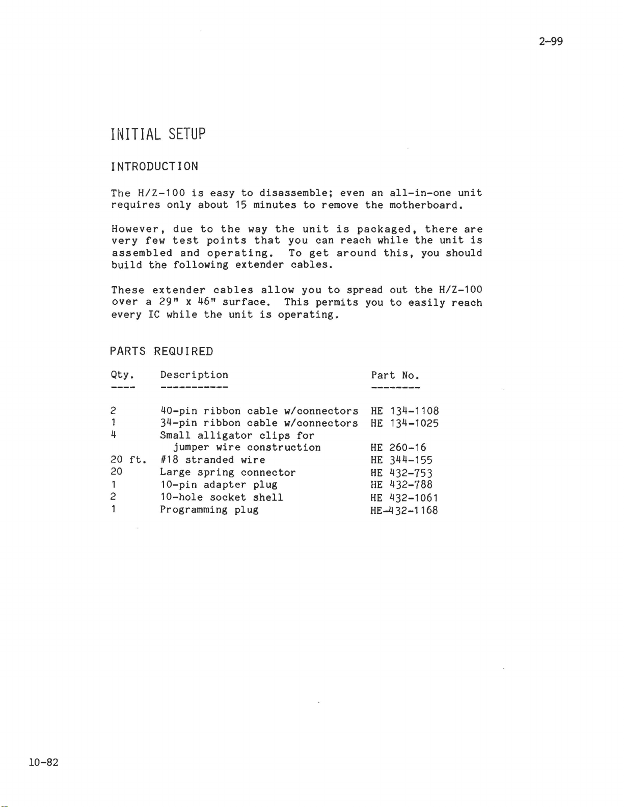
INITIAL
SETUP
INTRODUCTION
The
H/Z-100
requires
However,
very
assembled
build
These
over
every
few
the
extender
a
Ie
PARTS
Qty.
2
1
4
20
ft.
20
1
2
1
29"
REQUIRED
Description
40-pin
34-pin
Small
#18
Large
10-pin
10-hole
Programming
is
only
about
due
to
test
and
following
x 46"
while
alligator
jumper
stranded
spring
easy
points
operating.
the
ribbon
ribbon
adapter
socket
to
15
the
extender
cables
surface.
unit
wire
wire
connector
plug
disassemble;
minutes
way
that
allow
is
cable
cable
clips
construction
plug
shell
to
the
unit
you
To
cables.
you
This
operating.
w/connectors
w/connectors
for
remove
can
get
to
permits
even
is
packaged,
reach
around
spread
an
all-in-one
the
motherboard.
while
this,
you
Part
HE
HE
HE
HE
HE
HE
HE
HE-432-1168
the
out
the
to
easily
No.
134-1108
134-1025
260-16
344-155
432-753
432-788
432-1061
there
you
unit
are
unit
H/Z-100
is
should
reach
10-82
Page 4

Page 5
3-21
TEST,
by-t"ti'e"wait-for
23
waits
MN/MX,
pinplaces
by
of
1s
RESET,
The
8088
(program
below
This
is
and
to
READY,
signal
is
CPU
brings
memory
Pin
is
low,
in
the
the
used
interrupts
are
the
line
pull
the
the
8088.
ready
goes
or
an
Pin
H/Z-100.
pin
for
Pin
set
counter)
top
is
ed
low.
clock
Pin
from
to
into
it
high.
I/O
23
Test
execution
idle
state.
33
Minimum/Maximum:
the
8088
functions
larger
21
Reset:
are
or
cleared,
end
of
asserted
ASchmitt
circuits
22
the
addressed
transfer
a
wait
dev
ices.
test"
continues,
in
When
change.
systems
disabled,
points
the
Ready:
This
Input:
software
the
placed
Goes
to
1
when
retimes
data.
state
allows
This
otherwise
minimun
in
the
Usually,
and
multi-processing
high
certain
and
the
the
memory
megabyte
the
RESET
tr
igger
it
This
is
memory
When
until
using
input
instruction.
the
Logic
mode,
maximum
to
instruction
range
shapesthis
before
an
or
this
the
the
the
reset
registers
address
(FFFFOH).
line
acknowledgement
I/O
line
addressed
the
8088
is
examined
processor
one
on
mode
mode,
maximlDll
systems.
the
16
at
applying
port
is
low,
with
If
pin
this
used
some
mode
8088.
in
the
pointer
bytes
U236-11
signal
it
that
it
the
device
slow
10-82
The
READY
one
on
8088
to
This
the
processor
eLK,
for
is
clock
Pin
provide
signal
15-MHz
optimized
the
signal
U236-4.
to
19
timing
crystal
active
swap
is
ensure
8088
comes
timing
processor,
port
generated
U236
correct
Clock
to
the
from
at
as
when
synchronizes
set
Input.
8088.
U236-8
Y103.
inside
886
this
to
the
provide
U205-9
this
up
and
Five-megahertz
which
Duty
line
cycle
8088.
also
system
places
signal
hold
derives
When
times.
is
about
goes
timing.
a
with
it
the
to
logic
the
clock
from
33i
8088
the
Page 6

3-22
r--------------------------:~
1111.
......
-----------=
~-----'~~,....,U.,.,2~OJ
....
'<.ItI-L-D._('7'(I
D11H
lS'"
44J''''
.......
L IIl4Cll.O
MOL'·
~----~II.I>
..
IlEF·
IW"
ISWAP
"'01""*-+"'l
PORTI
Sllf~IHT
IML
51lL
••\.........
+-F~
"'-h;,q-~"
+--tt!.)~A:-;-L';.;;JT;--tI!P
P
•
""'04.
~---,P--st
PROCESSOR
SWAP
PORT
(MBl)
Page 7
3-23
PROCESSOR
SWAP
OVERVIEW
The
processor
handles
the
port,
three
mask,
the
interrupt
clock
the
bits
ADl
processor
PROCESSOR
Refer
At
This
responds
one
the
the
go
to
power
pin,
on
85HOLD
first
high,
schematic
U181-2.
disabling
swap
circuits
CPU
writes
of
the
controls
swap.
SWAP
up,
the
8SEL,
by
placing
line
positive
PORT
port
routing,
during
a
byte
reset
connects
On
will
are
the
swap
MBl
as
a
the
go
transition
the
8088
controls
the
control
used:
interrupt
you
circuits
to
logic
first
low,
cpu.
which
and
swap.
read
clear
U186-5,
zero
positive
enabling
of
ensures
byte
ADO
controls
line,
the
on
~,
CPU
is
proper
To
access
to
port
and
following.
U171-9
a 12H6
U181-12
the
to
transition
the
88HOLD
to
OFEH.
the
AD7
logic
PAL.
and
8085
be
active,
timing
the
interrupt
performs
This
a
of
CPU.
line
of
swap
Only
zero.
IC
l~c
85~,
On
will
The
8085,
transfers
bit
7
of
Here's
The
CPU
decoder)
U111-12.
As
a
result,
one.
The
respective
The
values
while
control
the
how
.•.
addresses
at
Finally,
8SEL
outputs,
executing
processor
U206-5.
Ul11-11
line
at
U172-12
to
the
swap
port
it
goes
is
now
and U172-2
but
these
the
8088.
OFEH
It
then
asserts
high
asserted.
code
port
to
will
in
It
control
assert
sets
the
and
are
be
the
does
SWAPCS
AD7
write
latches
also
covered
monitor
this
byte
to
line
U171-9
latched
to
(from
logic
later.
ROM,
by
logic
at
soon
setting
one.
the
one
U206-6.
to
logic
to
their
1/0
at
10-82
Page 8
3-24
The
8SEL
logic
to
change
The
HOLD.
S-100
to
disable
CPUs
the
happens.
turn,
The
control
respond
8088
board
one.
bus
raises
of
line.
U186-18
to
line
takes
both
at
U186
that
the
now
logic
at
control
the
by
returning
U186-3
asserts
the
S-100
generated
H/Z-100.
logic
to
change
one.
U185-11
8085
and
the
pHLOA
one.
of
and
the
the
causes
to
asserts
the
the
their
8085
HAK
line
line
HOLD·
U186-13
logic
H/Z-100.
8088
hold-acknowledge
zero.
whenever a
This
through
at
U171-2.
at
pin
to
logic
request
17.
one
to
change
and
U186-16
board
causes
U187. Both
can
signals;
When
This,
at
U180-9.
now
on
to
the
U186
this
in
take
SWAP
The 88SEL
This
system
to
is
The
clocks;
these
from
clock
circuits.
TIMING
circuit
the
no
longer
8085
clocks
one
clock
other.
line,
line
and
the
clock
also
is
designed
line
It
active
the
8088
8085 from
are
stable.
to
S~.
which
goes
when
also
when
run
Y101
another
to
to
the
H/Z-100
ensures
the
other
on
and
they
can
can
U188-4,
suppress
that
separate
the
aren't
cause
upset
a
switches
the
CPU
is
8088 from Y103.
a
the
quad
any
CPU
enabled.
crystal-controlled
in
glitch
D-type
glitches
being
phase.
on
timing
from one
Switching
the
in
latch.
on
the
CPU
disabled
Although
system
other
Page 9
3-25
10-82
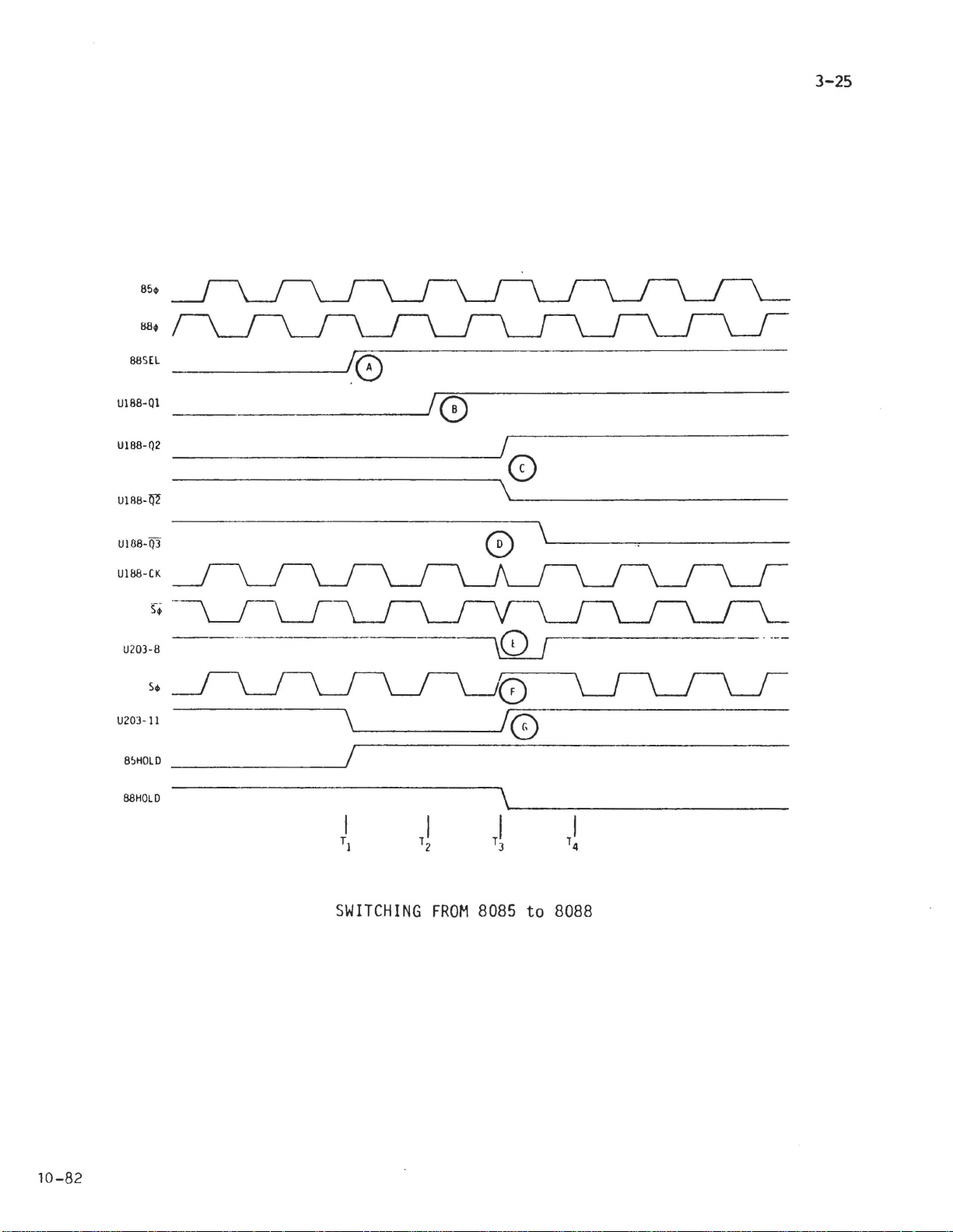
SWITCHING
FROM
8085
to
8088
Page 10
3-26
To
see
spike,
how
refer
U188 and
to
the
its
associated
waveforms on
the
circuits
previous
block
page.
this
The two
8085
inverters
the
through
U225B
At
logic
The
U188-2,
The
shown
gate
the
two
immediately
waveforms
Up
OR
Q2
since
same,
This
until
and
active
to
time
next
next
at
88~
clocks
until
gate,
and
forces
one
the
at
Q3
Q2
causing
time
top
waveforms
8088
the
clock
T1,
clock
clock
C.
U203B. At
clock
illustration.
this
has
went
CPUs.
U200-2
processor,
inverter
U188.
the
as
shown
pulse
Q1
output
pulse
This
to
are
nearly
returns
time,
been
of
U188
low
U203-8
the
T4
(waveform
8088
system
These
and
U200-14.
to
at
at
at
causes
tri-states
the
the
~
to
the
logic
have
at
time
are
the
are
then
is
l80-degrees
output
to
F).
form
selected;
A
on
U188-9
B.
same
line.
zero,
one.
been
T3,
go
clock
U200-1
the
to
respective
present
Assuming
Sl.
waveforms
latches
the
Q2
U200
time,
Since,
causing
of
U203-8,
This
in
opposite
both
logic
output
is
low
It
also
the
output
through
Q2
goes
in
out
of
the
is
inputs
zero
at
U225-3
clocks
at
that
and
couples
88SEL
this
the
this
phase,
spike
another
because
states.
to
for
the
inputs
the
8085
85'
couples
through
line
illustration.
logic
to
exclusive-DR
low
example,
U203C
(waveform
goes
one
latch
to
the
at
D
exclusiveits
However,
are
to
logic
couple
in
inputs
the
of
is
to
into
high,
the
clock
the
the
E).
one
Page 11
At
time
causes
gate
8088
As
U188
completely
To
illustration.
at
signal.
mentioned
perform
see
T4,
the
U225A
how
the
01
output
to
earlier,
is
disabled
this
first
pass
to
positive-going
of
the
the
ensure
before
is
done,
U188
system
other
that
again
the
to
edge
go
clock,
function
the
other
refer
high.
CPU
of
being
CPU
to
the
This
which
that
is
the
8088
disabled
activated.
clock
opens
is
now
88SEL
waveforms
3-27
the
the
and
is
Once
8085
which
exclusive-OR
inputs
to
Both
hold-acknowledge
the
17
At
logic
preset
zero
state.
Al
This
the
line
manufacturer.
8088
preset
8085
which
time
so
NDEF
again,
to
is
are
CPUs
one,
states.
at
at
last
that
is
the
coupled
both
respond
to
drives
T3,
U187-2
thi
IC
(8088)
can
active.
now
thus
s
assume
8088.
gate
the
HOLD
pin
the
the
into
time,
connects
be
For
that
At
to
is
the
same
latches
by
going
signals
4
through
S-100
Q2
line
releasing
The
next
U187-5,
U
188-7
line.
used
the
the
timeT1,
U203-11.
Q2
state,
at
into
to
U171.
pHLDA
goes
the
88l
removing
goes
to
pin
This
for
any
H/Z-100,
H/Z-100
the
The
line
U203-11
U187.
a
U186;
line
low
latches
clock
high
21
of
line
function
this
is
switching
from
HOLD
the
This
at
and
pulse
is
88SEL
other
U180-9.
the
to
the
a
line
line
U188.
goes
stat~
8088
asserts
U203-11
at
U187
latches
8088
drive
S-100
"not-to-be-defined"
by
asserts
input
to
to
from
U215-3
the
from
goes
of
Since
logic
and
pin
HAK
returns
from
the
the
bus
to
computer
when
the
high,
this
both
zero
sending
3
and
at
pin
their
logic
hold
high.
form
the
to
10-82
Page 12
3-28
INTERRUPT
The
interrupt
are
sent
is
set
processor
8085
is
ac
swap
the
8088
8088
Immediately
processor.
are
logic
U225-1
inverts
So
all
U189A.
The
8SEL
U1898
the
8085
and
5SEL
to
or
gets
t i
ve.
port
is
regardless
O.
shown
the
interrupts
non-maskable
line.
and
hands
will
MASK
mask
the
cleared
swap
all
interrupt
the
will
active.
after
Control
one.
resulting
U189C.
go low.
circuits
currently
port.
in
terrupt
disable
of
the
These
near
are
through
which
the
control
by
If
all
mask
reset.
lines
the
logic
sent
is
AND
ensure
active
setting
set.
requests.
request
the
8085
interrupt
bit.
the
5SEL
two
lines
8085
zero
to
U189D.
the
gates
to
the
that
CPU.
or
clearing
and
the
If
cleared.
is
blocked.
and
enable
requests
Here's
8085
at
U171-8 and
connect
IC
on
the
to
enable
the
8085;
complement
to
the
8088
CPU.
interrupt
The mask
bit
8085
hoW
CPU
is
the
are
it's
is
MSKatU112-6
to
schematic.
U189A
maskable
of
5SEL.
8088.
8SEL
requests
bit.
0
of
active,
and
the
However.
8088.
sent
will
to
done
.••
the
active
U225-9 and
U220-2
and
U189D.
through
disables
Later.
go
MSK.
the
the
8085
the
If
the
when
high
If.
while
zero.
interrupt
if
an
NMI,
U156-6
The
NMINT
port.
As
a
H/Z-100 swaps
When
and
U189C. U189A
logic
the
routed
U220-2
interrupt
The
result,
the
zero
R:rK
to
the
request
line
8088
bit
the
8085
disables
will
other
U155-8
to
CPU
at
at
BOB8
is
from
request
go
high
connects
input
the
is
and
U225-9.
U?25-10.
processor.
selected.
U189A
both
to
is
goes
8088
processor
active.
U189D
So,
and
the
should
assert
to
U155-9
the
low
no
all
the
MSK
U189D.
8085 and
occur.
the
MSK
line
to
assert
as
8SEL
are
disabled
matter
interrupt
line
the
either
NMINT
in
the
which
the
described
is
high
what
is
set
This
8088.
line.
processor
is
8SEL
to
enable
because
the
requests
to
logic
blocks
However.
standard
swap
also
line.
previously.
high.
U1898
5SEL
setting
will
the
or
The
is
of
be
Page 13
3-67
MAP
Map
but
SELECTING
selecting
two
lines,
currently
logic
state
BA12-BA15,
four
configurations
Configuration
In
appears
The
HP/H
takes
MAPSELO
are
of
U111-1 and
the
Confisuration
This
is
from0to
Confisuration
In
appears
The
This
the
unchanged.
the
this
to
two
configuration
8085
this
to
two
while
place
and
not
used
memory map
shown
11:
HAPSEL
default
192K.
configuration,
be
16K
areas
CPU.
configuration,
be
16K
This
running
confisuration,
12: HAPSELl = 0
swapped
and
13:
HAPSELl
swapped
areas
configuration
the
at
pins
MAPSEL1,
by
U111-15,
will
in
the
1 = 0
HAPSELO-=0
the
with
the
the
with
8085
= 1
the
the
rest
HAPSELO
the
CPU.
maybeused
and
1 and 15
also
this
IC.
plus
appear
illustration:
memory
HAPSELO
first
for
first
of
= 1
48K
RAH
HP/H
= 0
first
first
middle
alay
48K
64K
also
go
the
to
48K
are
of
48K
to
is
of
while
of
be
of
U111.
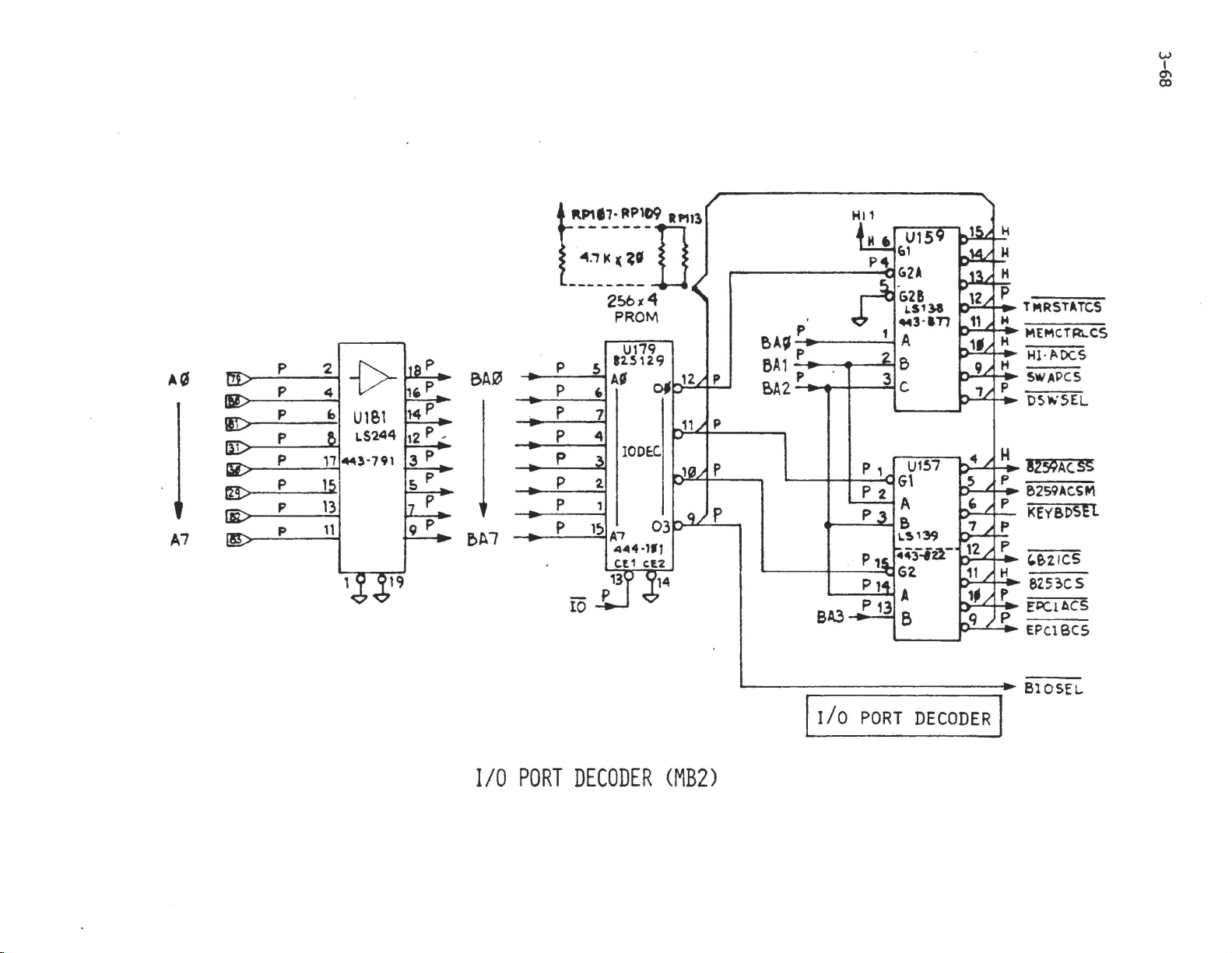
U173-7
Depending
address
be
in
one
contiguous
bank
zero
of
bank
runfling
zero
bank
RAH
1-
2.
are
for
unchanged.
bank
of
used
on
and
on
of
These
-8;
the
lines
the
Confisuration
In
swapped
above
does
using
Note
swapped
that,
from
addresses
asserts
For
a
example,
Configuration
the
6K
location,
memory
mind,
is
Address
keep
at
however,
concerned,
lines
some
increments.
this
configuration,
and
the
an
in
the
the
swapped memory,
different
assume
114.
the
70K
the
BA12-BA15
sections
14: HAPSELl = 1
with
5t>K
below
top
64K
extended
all
bank.
cases,
memory's
RAS
If
U111
would
location
that
as
byte
in
bank
each
56K
This
BIOS when
line
that
the
far
at
6K
allow
of
memory
56K
1.
area
configuration
running
the
point
the
than
the
CPU
assert
will
as
was
HAPSELO
in
= 1
bank0appears
four
kilobyte
remain
CP/H-85.
memory
of
memory
it
normally
H/Z-100
should
REN1
be
the
CPU
wri
tten
the
memory map
in
unchanged,
only
buffers
would
appears
view.
map
decoder
would.
is
write
to
instead
written
(and
the
to.
place--down
to
be
as
permit
When
the
operating
the
byte
of
RENO.
to.
Bear
programmer)
decoder
to
be
CPU
merely
in
at
The
in
to
to
4K
10-82
Page 14
w
Cl'l
CD
I
A~
/4.7
m>
m>
I
21{>~
U1Bl
LS'244
" p
14
12
3 P
& P
P
p
111
r
19
BA0
P
P ,
~~7
/
r.p!I_7:
~~'!'1
..
7·1~·
.'"3
n
--------
256'1.4
PROM
U179
_
10
82.~129
5
Af
,
1
4
100E:C
.3
2.
,
1~
A"7
"lolll4·1JI
C[1
iJ
12./
~
~
'1
'"
_1(21/
I"'"
.q/
..,-
03
CE2
~'4
P
P
P
P
P
P
P
P
P
P
P
P
p
BA~.
5A1
P
p.
BA2
-
BA3
HI1
-~
H •
P4
~
P 1
P 2
PJ
P,s.
Pl~
P
13
U159
(,1
G2A
G28
LS1H
~d·'n
1 A
,
B
3 c
U157
...
Gl
A
!>
~~'39
"43";U-
G2
A
8
"
l-I
1~
101
...\4.1
.13.
H
P
12
I""
11
~
1""1'
H
V
t!.
I""
p
1/
,..,
..
H
4/
p
5
,/
P
p
7
~2/
~
,..,
11/
H_
,_/
p-
~
...
q
~
T~RSTATCS
MEMCTRl,.CS
l"I1·ADCS
~WAPCS
D5~5EL
!Z39AC.~
~2S9AC.S'"
KEY8DSH
,"~ZIC5
8,5~CS
EPCl ACS
EPCl BCS
I/O
PORT
DECODER
CMB2)
I
I/O
PORT
DECODER
810SEL
r
Page 15
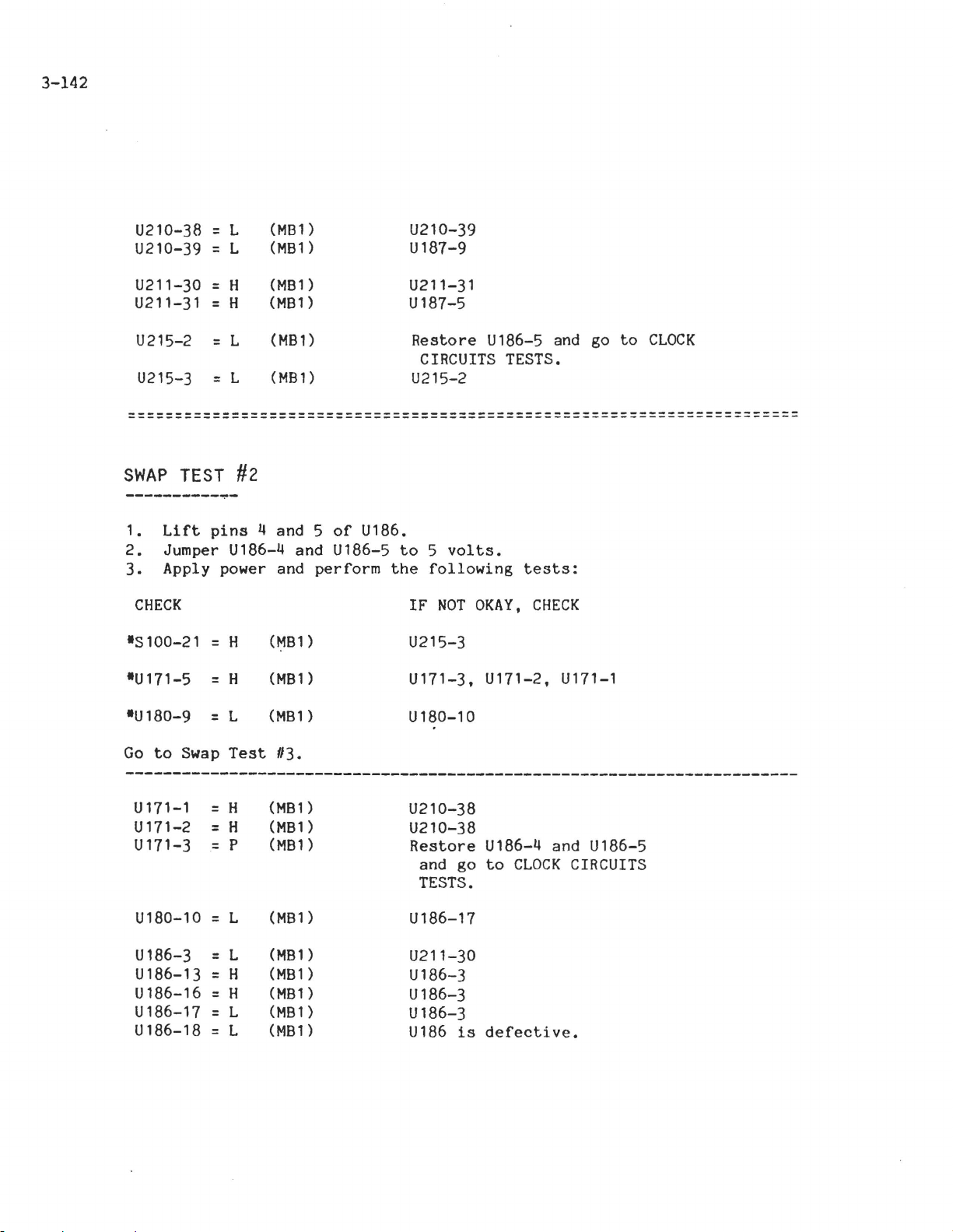
3-141
PROCESSOR
SWAP
1.
2.
3.
CHECK
·S100-21
·U180-9
·U186-3
·U186-4
Go
U17l-l
U171-5
TEST
Lift
Jumper U186-5
Apply power and
to
Swap
SWAP
#1
pin5of
= L
L
=
H
=
= L
Test
::
L
= L
TESTS
U186
to
ground.
perform
(MS1)
(MS1)
(MS1)
(MS1)
#2
(MS1)
(MS1)
(MS1).
the
IF
U215-3
UlaO-l0
U2l1-30
U17l-5
U2l0-38
U171-1
following
NOT
OKAY,
steps:
CHECK
U180-10
U186-3
U186-4
U186-l6
U186-17
U186-l8
U187-2
U187-3
U187-5
U187-9
U187-l0
U187-ll
U187-l2
U203-1l
U203-12
U203-13
::
=
::
=
=
=
::
=
=
= L
::
::
= L
::
::
::
(MS1)
L
(MS1)
H
(MS
L
L
L
H
H
p
H
H
P
H
L
H
1)
(MS
1)
(MS1)
(MS1)
(MS1)
(MS1)
(MB
1)
(MS
1)
(MS1)
(MS1)
(MS1)
(MS1)
(MS1)
(MS
1)
U186-17
U2ll-30
U171-5
U186-3
U186-4
U186
U186-l8
Restore
U187-2. U187-3
U187-10,
U203-l1
Restore
U186-3
U203-l2,
U186-l6
Restore
is
CIRCUITS
CIRCUITS
CIRCUITS
defective.
U186-5 and go
TESTS.
U187-ll,
U186-5 and
TESTS.
U203-l3
U186-5 and
TESTS.
to
U187-12
to
go
to
go
CLOCK
CLOCK
CLOCK
10-82
Page 16
3-142
L
H
H
L
L
#2
(MB1)
(MS
1)
(MS1)
(MS1)
(MS
1)
(MS
1)
4 and 5
(MS1)
(MS1)
of
U186.
perform
U210-38
U210-39
U211-30
U211-31
U215-2
U215-3
-----------------------------------------------------------------------
-----------------------------------------------------------------------
SWAP
1.
Lift
2.
Jumper U186-4 and U186-5
3.
Apply power and
CHECK
.S
100-21 = H
·U
171-5 = H
=L
=
=
=
=
=
TEST
pins
U210-39
U187-9
U211-31
U187-5
Restore
CIRCUITS
U215-2
to
5
the
following
IF
NOT
U215-3
U171-3, U171-2, U171-1
volts.
OKAY,
U186-5
TESTS.
tests:
and
CHECK
go
to
CLOCK
·U180-9
Go
to
Swap
U171-1 = H
U171-2
U171-3
U180-10=L
U186-3
U186-13
U186-16
U186-17=L
U186-18
= L
Test
= H
= p
L
=
H
=
H
=
L
=
(MS1)
#3.
(MS1)
(MSl
(MS1)
(MS1)
(MS
1)
(MS
1)
(MS1)
(MS
1)
(MS1)
U180-10
U210-38
)
U210-38
Restore
and go
TESTS.
U186-17
U211-30
U186-3
U186-3
U186-3
U186
is
U186-4 and U186-5
to
CLOCK
defective.
CIRCUITS
Page 17
3-143
U187-2
U187-3
U187-4
U187-5
U187-9
U187-11
U187-12
U203-11
U203-12
U203-13
U210-38
U210-39
U211-30
U211-31
U215-2
U215-3
=
=
=
=
=
=
=
=
=
=
=
=
=
=
=
= L
(MB1)
L
p
(MB1)
(MB1)
H
(MB1
(MB1)
(MB1)
(MB1
(MB1)
(MB1)
(MB1)
(MB1)
(MB1)
(MB1)
(MB1)
(MB1
(MB1)
)
)
)
L
H
P
H
H
H
L
H
H
L
L
H
U186-18
go
go
U186-4
to
CLOCK
U186-4
to
CLOCK
U203-12
U186-4
to
CLOCK
U186-4
to
CLOCK
Restore
and go
TESTS.
U203-11
U187-2_ U187-3_
U187-11_ U187-12
Restore
and
TESTS.
U186-13
U203-13_
U186-16
Restore
and
TESTS.
U210-39
U181-9
U211-31
U187-5
Restore
and go
TESTS.
U215-2
and U186-5
CIRCUITS
U187-4
and U186-5
CIRCUITS
and U186-5
CIRCUITS
and
U186-5
CIRCUITS
10-82
======================================================================
SWAP
1.
2.
3.
4.
5.
·U180-9
Go
TEST
Restore
Jumper U186-5
Turn on
Connect
S-100
Perform
CHECK
= H
to
Swap
#3
pin4of
to
the
H/Z-100.
a jumper
bus (HOLD·).
the
following
(MB
1)
Test
#4.
U186;
ground.
wire
from ground
tests:
leave
IF
U180-10
pin
NOT
5
lifted.
to
pin
OKAY_
74
CHECK
of
..
the
Page 18
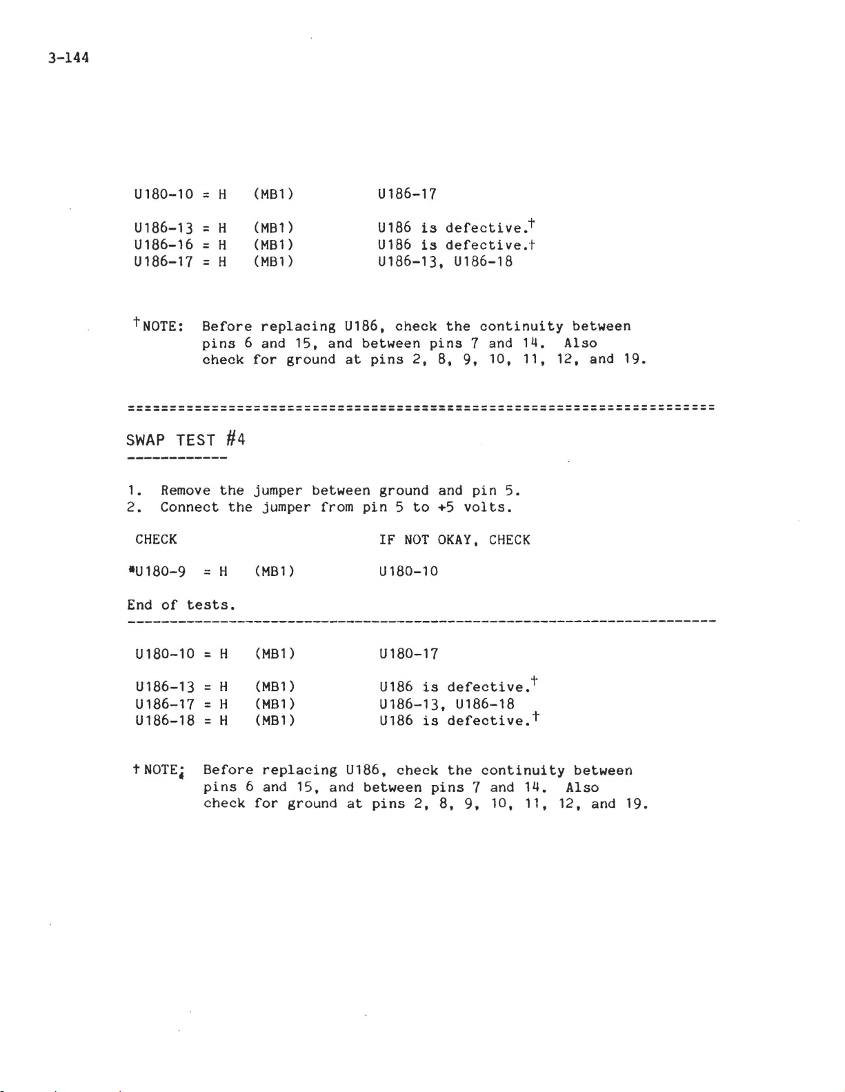
3-144
U180-10 = H
U186-13
U186-16
U
186-17
tNOTE:
=H
= H
= H
Before
pins
check
(MB1)
(MB1)
(MBl
(MB1)
replacing
6 and
for
)
15.
ground
and
U186-17
U186
U186
U186-13. U186-18
U186.
between
at
pins
is
is
check
pins
2.
defective.
defective.t
the
continuity
7 and
8.
9.
10.
t
between
14.
Also
11. 12. and
19.
===============;======================================================
SWAP
1.
2.
.U180-9
Remove
Connect
CHECK
TEST
=H
#4
the
the
jumper
jumper from
(MB1)
between
ground
pin
IF
U180-10
5
NOT
to
and
pin
+5
volts.
OKAY.
5.
CHECK
End
of
tests.
U180-10 =H
U186-13
U
186-17
U186-18
tNOTE.
= H
= H
=H
Before
pins
check
(MB1)
(MB1)
(MB1)
(MB1)
replacing
6 and
for
15,
ground
and
U180-17
U186
U186-13. U186-18
U186
U186.
between
at
pins
is
is
check
pins
2.
defective.
defective.
the
continuity
7 and
8,
9,
t
t
14.
10. 11,
between
Also
12,
and
19.
Page 19
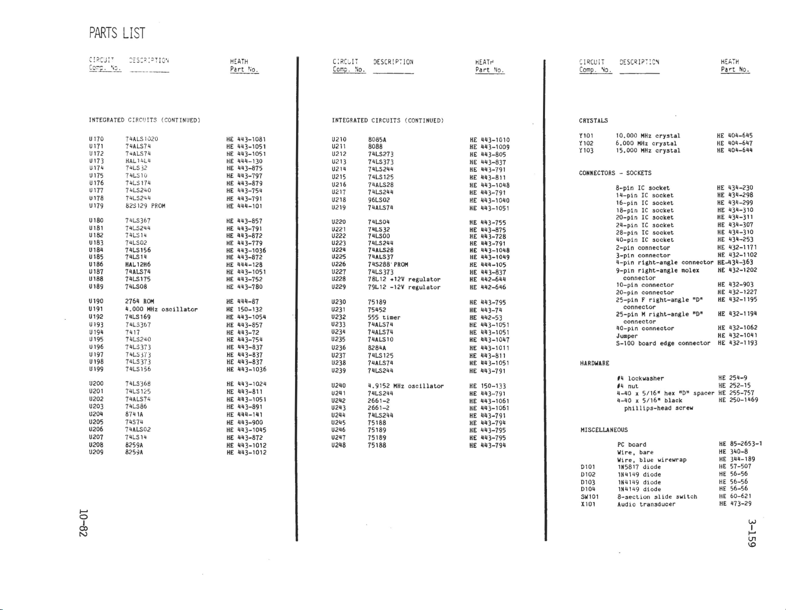
PARTS
C!
~~
?CJ
LIST
1~,..
:':5:':
:Tl~'i
HEATH
Part
';0.
c:
;lCe
Com?
IT
~Io.
DESCRIP710:/
HEAT"
Part
:/0.
CIRCUIT
Compo
OESCRl?i!C~
~O.
HEl,iH
Part
No.
INTEGRATED
U
170
U171
U172
UI73
U174
U175
U176
U
177
U178
U179
U180
U181
Ul82
u183
U184
u185
U186
U187
U188
U189
U190
U191
U192
U193
U194
U195
U196
U197
U198
U199
U200
U201
U202
U203
U204
U205
U206
U207
U208
U209
.......
0
I
CO
N
CIRCUITS
74ALS1020
74ALS74
7"ALS74
HAL14L4
74LS32
74L510
74L5174
74LS240
74LS244
825129
74LS367
74LS244
74L514
7"LS02
74LS156
74L514
HA1.12H6
74ALS74
74LS175
741.S08
2764
ROI1
4.000
HHz
74L5169
'!4U367
7417
74L5240
74L5373
741.Sfl3
74LS373
741.S156
74LS368
74L5125
74A1.S74
74LS86
8741A
74S74
74ALS02
74LS14
8259A
825~A
(CONTINUED)
PROM
oscillator
I
HE
443-1081
HE
443-1051
HE
443-1051
HE
444-130
HE
443-875
HE
443-797
HE
443-879
HE
443-754
HE
443-791
HE
444-101
HE
443-857
HE
443-791
HE
443-872
HE
443-779
HE
443-1036
HE
443-872
HE
444-128
HE
443-1051
HE
443-752
HE
443-780
HE
444-87
HE
150-132
HE
443-1054
HE
443-857
HE
443-72
HE
443-754
HE
443-837
HE
443-837
HE
443-837
HE
443-1036
HE
443-1024
HE
443-811
HE
443-1051
HE
443-891
HE
444-141
HE
443-900
HE
443-1045
HE
443-872
HE
443-1012
HE
443-1012 Wire. bare
INTEGRATED
U210
U211
U212
U213
U214
U215
U216
U217
U218
U219
U220
U221
U222
U223
U224
U225
U226
U227
U228
U229
U230
U231
U232
U233
U234
U235
U236
U237
U238
U239
U240
U24'
U242
U243
U244
U245
U246
U247
U248
- -
CIRCUITS
8085A
8088
74LS273
74LS373
74LS244
74L5125
74ALS28
74LS244
96LS02
74ALS74
74LS04
74L532
74L500
74L5244
74ALS28
74AL537
74S288'
74LS373
781.12
791.12
75189
75452
555
timer
74ALS74
74ALS74
74ALS10
8284A
74LS125
74ALS74
74LS244
4.9152
74L5244
2661-2
2661-2
74LS244
75188
75189
75189
75188
(CONTINUED)
PROM
.12V
regulator
-12V
regulator
MHz
oscillator
HE
HE
HE
HE
HE
HE
HE
HE
HE
HE
HE
HE
HE
HE
HE
HE
HE
HE
HE
HE
HE
HE
HE
HE
HE
HE
HE
HE
HE
HE
HE
HE
HE
HE
HE
HE
HE
HE
HE
443-1010
443-1009
443-805
443-837
443-791
443-811
443-1048
443-791
443-1040
443-1051
443-755
443-875
443-728
443-791
443-1048
443-1049
444-105
443-837
442-644
442-646
443-795
443-74
442-53
443-1051
443-1051
443-1047
443-1011
443-811
443-1051
443-791
150-133
443-791
443-1061
443-1061
443-791
443-794
443-795
443-795
443-794
I
I
CRYSTALS
YI01
YI02
Y103
CONNECTORS-SOCKETS
HARDWARE
HISCELLANEOUS
0101
0102
0103
0104
SW101
Xl01
10.000
6.000
15.000
8-pinICsocket
14-pinICsocket
16-pinICsocket
18-pinICsocket
20-pinICsocket
24-pinICsocket
28-pinICsocket
40-pinICsocket
2-pin
3-pin
4-pin
9-pin
10-pin connector
20-pin
25-pin
25-pinHright-angle
40-pin
Jumper
S-10D
14
14
4-40 x
4-40 x
PC
Wire, blue wirewrap
IN5817
IN4149
1N4149
1N4149
8-section
Audio
I I
MHz
crystal
MHz
crystal
MHz
crystal
connector
connector
right-angle
right-angle
connector
connector
Fright-angle
connector
connector
connector
board edge connector
lockwasher
nut
5/16"
hex
5/16"
phillips-head
board
black
diode
diode
diode
diode
slide
transducer
HE
404-645
HE
404-647
HE
404-644
HE
434-230
HE
434-298
HE
434-299
HE
434-310
HE
434-311
HE
434-307
HE
434-310
HE
434-253
HE
432-1171
HE
connector HE-434-363
molex
"0"
"0"
"0"
spacerHE255-757
screw
switch
HE
HE
HE
HE
HE
HE
HE
HE
HE
HE
HE
HE
HE
HE
HE
HE
HE
HE
HE
HE
432-1102
432-1202
432-903
432-1227
432-1195
432-1194
432-1062
432-1041
432-1193
254-9
252-15
250-1469
85-2653-1
340-8
344-189
57-507
56-56
56-56
56-56
60-621
473-29
w
I
t-'
lJ1
\.0
Page 20

Page 21
::::::::::::::::::::::::::;:;:::;::::::::::::::::::.
":;:::::::::::::::;'
.........
.li
.:->:-:-:.:-:-:-:
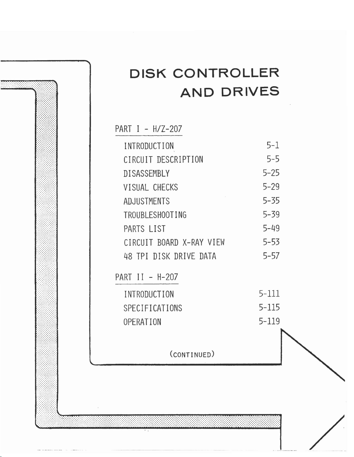
DISK
PART
I -
CONTROLLER
AND
H/Z-207
DRIVES
II
.........
·........
. ..... .
·.
.........
.........
· .
·........
· .... ....
..................
........
·.. . . ....
·.... ....
-:-:-:.:-:-:-:-:-:
.........
· .
.....
....
·........
·.. .. . . . .
.........
·. .. .... .
........
' .
..................
..................
.'';-:'>:-:-:':-'
· ........
.........
.........
· .
..................
INTRODUCTION
CIRCUIT
DESCRIPTION
DISASSEMBLY
VISUAL
CHECKS
ADJUSTMENTS
TROUBLESHOOTING
PARTS
CIRCUIT
48
PARTII-
TPI
LIST
BOARD
DISK
H-207
X-RAY
DRIVE
DATA
INTRODUCTION
SPECIFICATIONS
VIEW
5-1
5-5
5-25
5-29
5-35
5-39
5-49
5-53
5-57
5-111
5-115
..................
..................
. .. .... ..
· .
.......
..
:
~:):
~;
~:~;
~:~:~;
..........
·.. ......
.... . . . ..
><?::::)
...................
......
· .
..........
·. . . .....
..........
..................
.
OPERATION
(CONTINUED)
5-119
/
Page 22

Page 23
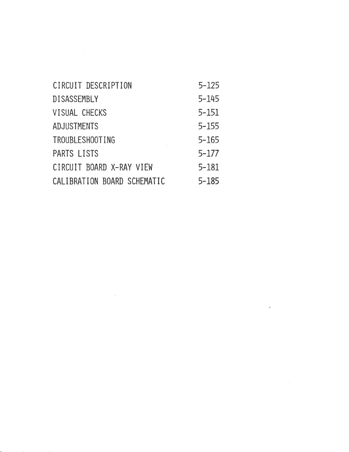
CIRCUIT
DESCRIPTION
5-125
DISASSEMBLY
VISUAL
ADJUSTMENTS
TROUBLESHOOTING
PARTS
CIRCUIT
CALIBRATION
CHECKS
LISTS
BOARD
X-RAY
BOARD
VIEW
SCHEMATIC
5-145
5-151
5-155
5-165
5-177
5-181
5-185
Page 24

Page 25
PART
INTRODUCTION
I
/
Page 26

Page 27
PART
INTRODUCTION
II
/
Page 28

Page 29
The
H-207
as
an
intelligent
drives.
multi-drive
and from
The
H-207
disk
controller
controlled
board
into
This
while
the
takes
the
type
the
work
is
a
floppy
The
system
the
disk
operates
by
the
commands from
necessary
of
system
disk
of
controller
controlling
interface
H-207
drives.
board
master
disk
selects
and
as
a
contains
signals
allows
the
controller
between
properly
slave
CPU.
the
required
the
board
disk
the
handles
processor.
its
own
Thus,
master
master
processor
drives.
board.
the
correct
processor
the
CPU
to
control
CPU
CPU
data
and
to
It
and
drive
This
disk
converts
do
actually
functions
the
transfer
means
which
controller
the
drives.
other
disk
in
the
them
tasks
does
5-113
a
to
is
The
H-207
and
of
drive
present
to
three.
The
H-207
State,
four
is
8"
used
Heath
can
Polled
controller
so
ft-sectored
the
board
Because
card,
the
controller
selectable
Shugart
it
IEEE
can
the
can
Standard.
board
addressing,
compatible
precompensation.
The
in
formation
familiarize
the
H-207.
troubleshoot
level.
versatile.
disk
and
Company
be
I/O,
board
disk
be
jumpered
H-207
be
installed
provided
you
with
Using
the
drives.
the
software
operated
or
Interrupt.
to
formats.
is
a IEEE
Additional
acceptable
software
8"
the
this
disk
information,
controller
It
User
density
in
support
to
operate
in
other
interface,
in
this
operation
can
limits
three
By
696
to
software
of
using
other
section
support
the
up
media.
the
different
This
almost
the
at
speeds
Standard
makes
of
features
computers
controllable
and
of
and
troubleshooting
you
board
to
to
four
selects
number
modes;
allows
all
Wait
State
up
S-100
computers
that
formatting,
adjustable
the
manual
will
the
5-1/4"
the
type
However,
of
drives
Wait
the
disk
available
mode,
to
6
MHz.
compatible
using
make
are:
user
will
be
able
component
the
of
to
10-82
Page 30

Page 31

SPECIFICATIONS
."
'.~
."
.... .
/
Page 32

Page 33
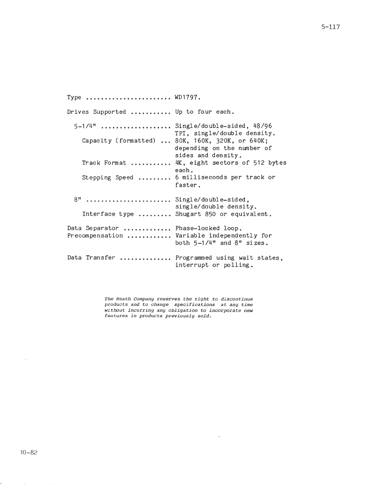
5-117
Type
Drives
••.••..•.••••..••••..••
Supported
5-1/4"
.•.••.•.••.••.•••••
Capacity
Track
Format
Stepping
8"
......•••..•..•...•....
Interface
Data
Separator
Precompensation
Data
Transfer
•••...•••.•
(formatted)
.•••.••.•..
Speed
type
•••••••••
......•••
.•....•••••••
.....•.••••.
•.••••.•••••••
WD
1
797
.
Up
to
four
Single/double-sided,
TPI,
•••
80K, 160K, 320K,
single/double
depending
sides
4K,
and
eight
each.
6
milliseconds
faster.
Single/double-sided,
single/double
Shugart
850
Phase-locked
Variable
both
5-1/4"
Programmed
interrupt
each.
density.
or
on
the
number
density.
sectors
per
of
track
density.
or
equivalent.
loop.
independently
and 8"
using
or
polling.
sizes.
wait
48/96
640K;
512
for
states,
of
bytes
or
10-82
The
Heath
products
without
features
Company
and
to
incurring
in
products
reserves
change
any
specifications
obligation
previously
the
right
sold.
to
incorporate
to
discontinue
at
any
time
new
Page 34

Page 35
OPERATION
INTRODUCTION
CLOCK
INTERRUPT
SLIDE
OUTPUT
5"
8"
SPEED
JUMPERS
SWITCH
CONNECTORS
Disk
Disk
(DS1)
Drive Connector
Drive Connector
5-121
5-121
5-122
5-122
5-124
5-124
5-124
./
Page 36

5-120
N
J
Page 37

INTRODUCTION
To
permitthe
computers,
incorporated
permit
environment
t h r e e ma
selection
switch,
for
configuring
the
location
DS1.
ina
a
in
of
H-207
number
into
rea
interrupt
the
which
s 0 f
Refer
of
the
to
of
design
the
the
concern:
jumpers
to
jumpers
operate
jumpers
of
controller
H-207
the
pictorial
and
in
is
and
many
and
the
board.
board
installed.
c10 c k s
the
setting
on
the
slide
different
a
slide
for
pee
the
switch
These
the
There
d j
urn
of
adjacent
switch.
types
devices
computer
per
i ng ,
the
slide
page
5-121
of
are
are
CLOCK
The
wi
J1
(See
to
than
installed
host
th
is
is
illustration
operate
3
SPEED
jumpered
MHz.
Jl
For
the
speed
bealtered.
on
jumper
Refer
al
at
the
to
teration.
bottom
from
computer
determined
by
in
computers
This
in
a
H/Z-100.
FOIL
I
,
O:':D 0
H-207
or
to
slower
This
of
the
the
illustration
CUT
FOILONBOTTOMOFBOARD
clock
by
a
foil
below.)
jumpering
JUMPER
operate
than
is
accomplished
the
circuit
middle
speed
the
that
Jl
or
in
3
hole
that
jumpering
run
on
This
set
for
jumpering
haveaCPU
is
for
CPU
a
computer
MHz,
board
of
below
the
at
the
bottom
normal
H/Z-IOO
clock speeds
the
by
J1
Computer
that
jumpering
cutting
and
installing
to
when
the
H-207
J1.
of
enables
clock
when
the
operation
faster
has
the
rightmost
performing
will
As
received,
the
the
speed
than 3
a
CPU
of
foil
a 1"
operate
board.
H-207
faster
H-207
MHz.
clock
J1
jumper
hole.
is
must
wire
this
10-82
Jl
Jl
setting
clock speed.
for3MHzorslower
CPU
Page 38

5-122
INTERRUPT
The
Vectored
on
the
The
data
holes
center
interrupt
line.
7.
from
No
is
when
interrupt
determined
J3
IRQ.
When
the
jumpers
used
the
JUMPERS
Interrupt
lower
request
through
row
of
lines
from
jumpered,
1797
are
in
a
HlZ-100.
H-207
protocol.
by
the
VI
VECTOR
(No
H/Z-100
INTERRUPT
jumpers are
operation.)
JUMPER
installed
left-hand
line.
J10
holes
VIO
the
these
controller
installed
is
customer's
LOCATIONS
for
jumper
corner
ORQ.
shown
numerically
through
1797
installed
The
in
is
locations
to
in
These
configuration
computer
locations.
of
the
from
VI7.
connected
these
jumper
0 0 0 0 0
0
0 0
the
the
correspond
the
S-100
in
computers
0
1797
illustration
The
route
locations
locations
documentation.
0 0 0
0 0 0
VI.
controller
is
connected
with
interrupt
to
holes
IRQ
interrupt
when
are
that
of
the
0
0
0
are
located
below.
the
request
0
through
and/or
the
only
require
jumpers
0 0
0
0
0
0
board.
The
S-100
ORQ
lines.
H-207
used
....
VI0-VIl
to
is
SLIDE
OSl,
and
sections
llH
OFF
an
the
I l 6 5
(l)
(0)
\
"------_-I
SWITCH
8-section
condition
of
I
<DSl)
OS1are
PORT
ADOllESSING
slide
of
defined
~
switch,
bits
-,
as
I
3 and 4
NOT
USED
3 2 I
o 1 2 3 4 5 6
determines
of
follows:
PRECOMP.
the
TPI
the
status
0.\
Configured foranH/Z-IOO
with48TPI. 5-1/4" Drives
port
port.
7-IRQ
address
The
Computer
~~~B8~~~
'.n
AT
0
DSI
I
Page 39

DSI
5-123
HEATH
Section
0
1
2
3-4-5-6-7
SOFTWARE
The
H-207
addresses.
1797
The
BOH.
registers,
H/Z-100
A map
DEFINED
Definition
This
bit
the
TPI
disk
drive.
o =
118
1
= 96
This
bit
whether
onoroff.
o = precomp
1 = precomp
Not
used.
Port
addressing.
occupies
The
three
computer
of
the
determines
of
the
TPI.
TPI.
determines
precomp
off.
on.
a
block
the
control
series
I/O
port
5-1/11"
3-4-5-6-7
is
of
low-order
place
is
Section
0
1
2
eight
bits
latch,
the
shown
contiguous
in
or
H-207
below.
niti
Status
Status
Not
Port
used.
DEFINED
on
port
port
addressing
HARDWARE
Defi
I/O
this
block
the
status
at
port
address
bit
bit
Leave
port
select
port.
ll.
3.
at
(HSB).
O.
10-82
ADDR.
dip
the
is
(Binary)
switch
bits
swi
shown
The
equi
for
dip
val
the
I/O
SSSSSOOO·
SSSSSOOO
SSSSS001
SSSSS010
SSSSS011
SSSSS100
SSSSS101
• S
switch
ent
of
HIZ-100
SSSSSXXX**=10110XXX=Port
** X = 1797
register,
control
bit
are
tches.
below.
JlEAD
•
•
•
•
•
simply
latch,
WRITE
•
•
•
•
•
For
BO
PORT
DESIGNATION
1797
1797
Command
1797 Track
1797
Sector
1797 Data
Control
-Status
defined
exqrnple,
- B7.
or
status
Status
Latch
Port
Register
Register
Register
Register
from
the
Register
the
port
port.
binary
address
Page 40
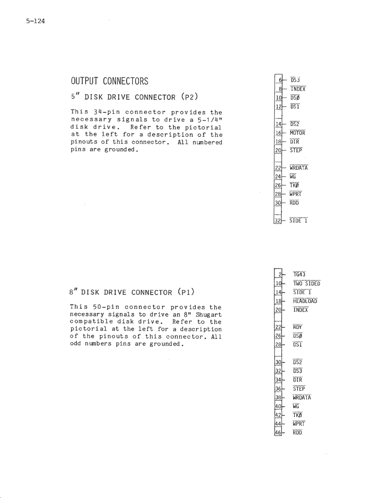
5-124
OUTPUT
5"
DISK
This
CONNECTORS
DRIVE
34-pin
necessary
disk
at
pinouts
pins
the
are
drive.
left
of
grounded.
connector
signals
for
this
CONNECTOR
to
drive
Refer
connector.
to
a
description
the
(P2)
provides
a
pictorial
All
numbered
the
5-1/4"
of
the
6
8
10
12
14
16
18
20
22
24
26
28
30
OS)
INDEX
DS0
DST
DS2
MOTOR
D1R
STEP
WRDATA
WG
TK~
WPRT
ROD
8"
DISK
This
DRIVE
50-pin
necessary
compatible
pic
tori
al
of
the
pinouts
odd numbers
connector
signals
disk
at
the
pins
CONNECTOR
provides
to
drive.
left
of
are
drive
this
grounded.
an 8"
Refer
for
a
connector.
(PI)
Shugart
to
description
the
the
All
32
22
26
28
30
32
34
36
38
40
42
44
46
SIDE
1
TG43
HiO
SIDED
SIDE
1
HEADlOAD
-INDEX
ROY
DS~
DS[
DS2
OS3
DIR
STEP
WRDATA
WG
T~
WPRT
ROD
Page 41

CIRCUIT
..
DESCRIPTION
1<:
BLOCK
DETAILED
DIAGRAM
S-100
Data
Data
CIRCUIT
Bus
In
Out
DESCRIPTION
DESCRIPTION
Interface
Address Lines
Control Lines
Vector
Ready
Interrupt
Line
Lines
RESETCIRCUITS
Power-Up/Reset
Power-Up
Write Protection
CPU/Controller Logic
Read
Status Latch
Read
Status Register of
Write Control Latch
(U31)
(U30)
Write Control Register in the
Data
ROY
Read/Write Operations 5-134
Delay
Interrupts
CONTROLLER/DISK-DRIVE
Data
Shaping 5-136
Data
Separation
Head
1797
8"
5"
CALIBRATION
H-207
Load
Timing
Drive
Drive
FLOPPY
Timi
ng
Interface
Interface
CIRCUIT
DISK
LOGIC
Precompensation
and
BOARD
CONTROLLER
1797
(U22)
1797
BOARD
(U22)
DEFINITIONS
5-127
5-128
5-128
5-128
5-128
5-128
5-128
5-129
5-129
5-129
5-129
5-130
5-130
5-130
5-131
5-132
5-133
5-135
5-135
5-136
5-136
5-138
5-139
5-139
5-139
5-140
5-141
"
,",
.
'.
..
::
.
" .
/
Page 42

~
l.I
~
~
~
~
~
~
c;
~
~
~
c;
~
~
~
V'
~
/
~
~
'/
~
~
~
~
~
'/
~
~
~
/
~
~
~
~
'/
V
~
'/
~
'/
~
~
~
~
~
'/
~
'/
~
~
~
~
'/
~
u.J
L>
<C
U-
0:::::
u.J
t-
z:
-
U)
::::>
.~
C>
C>
rl
U)
I
./
"
./
...........
~
~
~
~
~
~
/:
~
~
~
~
'/
"
~
~
~
~
,~
/~
~
~
~
~I
/"
STATUS
PORT
~
CONTROL
LATCH
IT»
./
"
./
"-
./
"'-
/
\
~
~
.......
.".
~
~
~
V
~
~
1797
FLOPPY
DISK
CONTROLLER
~
~
~
~
~
~
~
/
~
/
V )
~-
"
./
...........
~
~
~
~
u.J
~
L>
'/
<C
U-
~
0:::::
~
.......
u.J
,
""
......
......
.........
~~
/
\
~
.~
SEPARATION
~
~
~
,
PRECOMPEN-
/
~
SATION
'/
~
~
V1
/
\
DATA
AND
WRITE
./
"
'v
"''/
......
......
......
.......
~
~
~
~
~
~
~
~
~
~
~
'/
~
~
~
~
~
~
/'
~
~
/
~
/
~
~
~
t-
:z:
-
:::
00
u.J
<.J
<C
u..
0:::::
w
t-
z:
-
:::
Ll't
H-207
BLOCK
DIAGRAM
10-82
Page 43

5-127
BLOCK
Refer
The
major
control
separation
drive
The
octal
miscellaneous
interface
The
the
includes
disk,
The
as
the
The 1797
on
the
read
DIAGRAM
to
the
H-207
sections:
latch,
interfaces.
bus
interface
tri-state
status
status
and
control
DRIVE
selection
the
diskette.
formation
data
DESCRIPTION
H-207
Floppy
&
the
H-207
port
of
track
if
precompensation
latch
SELECT,
and mode
controller
is
controlled
the
write
enabling
the
density,
of
block
Disk
the
latch,
is
5"
written
diagram
controller
bus
interface,
1797
precompensation
is
to
a
disk
accepts
FASTEP,
That
floppy
made
an
the
S-100
read-only
drives
number
of
the
controls
is,
data,
by
the
up
address
circuitry.
is
commands
and
drives.
the
1797.
as
you
board
disk
of
two
bus
in
device
and
the
of
recording
being
to
others
the
placement
movement
and
read
the
controller,
circuits,
octal
comparator,
the
used.
the
that
the
the
consists
status
bus
These
H/Z-100.
that
controller.
disk
have
of
of
the
separation
following.
of
port,
the
and
the
buffers,
and
components
tells
sides
the
drives
to
do
information
drive
seven
data
some
This
to
such
with
head,
of
the
two
an
CPU
the
the
10-82
The
data
control
di
sket
clock
data
The
circuitry.
during
8"
interface.
separation
how
te
.
signal
and
It
the
5.25"
Up
and
the
data
does
during
double-density
drive
to
thisby
read
interfaces
four
write
is
read
se
operations
drives
precompensation
to
or
parati
write
can
ng
operations.
include
be
and
connected
circuitry
written
the
data
precompensating
buffers
from
from
and
to
the
the
filter
each
Page 44

5-128
DETAILED
S-100
The
S-100
696-standard
in
the
lines.
DATA
Data
through
bus
the
is
bus
DATA
Data
through
interface
U35.
not
The
da
latched
through
latches
into
interface.
status
buffered
by
out
present
tri-state
tab
CIRCUIT
BUS
IN
means
OUT
The
INTERFACE
Bus
appendices
the
signal
1
from
pins
plug.
latch
us
sot
in
U35
pin
an
asserted
atch
from
of
long
DESCRIPTION
Interface
S-100
35, 36,
1 when
Bus. See
of
this
bus
(out
lines
These
the
U36, a 741$244
the
is
latch
hat
on
pins
or
from
board's.
bus
38, 39,
This
used
enough
holds
the
every
the
sOUT
91-95
from
(into
data
because
for
1797
write
ALE
(Status
is
the
manual
the
and
are
the
internal
buffer.
the
40,
is
the
the
can
(Address
compatible
S-100
for
controller
signal
used
1797
data
cycle.
in
controller.
controller
88,
latched
data
1797
on
read
Out)
data
89,
signal
with
specification
definitions
board)
lines
read
and
by
on
to
the
it.
The
Latch
receive
41-43
operations
bus
to
board)
90
tri-state
the
S-100
board's
Va
1 i d dat a
latch
Enable)
via
any
travels
The
the
travels
on
the
properly.
internal
is
enabled
U20.
IEEE
sheets
of
the
on
the
from
data
S-100
bus
latch
bus
signal
is
is
ADDRESS
The
address
29,
30,
They
are
CONTROL
The
control
pins
face.
24,
These
LINES
lines
31,
79,
buffered
LINES
lines
25,
45. 46,
lines
from
and
by
from
are
the
80
the
the
and
buffered
bus
through
74LS244
S-100
75
enter
83
chip,
bus
through
by U33.
the
of
U34.
enter
78
board
the
the
of
bus
board
the
through
interface.
through
bus
pins
inter-
Page 45

5-129
VECTOR
The
at
pins
driven
READY
The
interface.
this
operations
operation.
RESET
INTERRUPT
vector
by U32.
4
through
interrupt
LINE
ready
line
line,
It
to
to
CIRCUITS
is
put
POWER-UP/RESET
On
power
to
the
control
U26
the
board.
flip-flops
up,
H-207
latch,
the
board
drivert
give
CPU
the
in
LINES
lines
11
of
RDY,
.
a known
enters
the
the
sends
This
write
from
the
by U32. The
CPU
controller
RESET*
pI
precompensation
state
bus
through
in
aces
the
interface.
a
wait
the
before
bus
pin
controller
state
time
through
1797
enter
72
during
to
the
controller,
control,
the
CPU
the
They
of
board
finish
S-100
board
may
the
bus
uses
some
the
bus
the
and
the
accesses
be
10-82
In
the
03H,
register
After
restore
o
and
is
found.
The
to
clear
The
the
sheets)
Finally,
an
RDY
·of
the
U27-11.
1797,
the
sector
(Not
the
reset
command. The
sends
See
reset
reset
phase
line
all
state
four
.
the
(ready)
qualification
the
Ready
an
the
of
U26
reset
register
bit)
line
interrupt
1797 IC
connects
the
outputs.
of
the
(¢4)
Q-outputs
signal
line
to
goes
drive
to
phase
input
to
needed
sets
to
01H,
logic
high,
read/write
to
the
data
sheets
pin1of
lock
equal
are
made
the
CPU
for
the
and
zero.
the
computer
for
the
loop
to
0
(see
equal
and
read/write
command
bit
7
1797
head
once
more
control
control,
the
to
1;
pin
5
enabling
register
of
the
executes
seeks
the
details.
latch,
U1,
1691
pin
provides
at
status
the
track
track
U30,
makes
IC
data
9
sends
part
through
Page 46

5-130
POWER-UP
On
power
until
could
any
disks
To
protect
1797
These
remain
4
are
whenever
is
volts.
biased
WRITE
up,
the
power
generate
that
the
coupled
transistors
cut
off
When
near
WG
is
the
a
may
disk,
until
the
asserted.
CPU/CONTROLLER
Reading
of
information:
signals,
read
and
and
writing
and
control
control
signals
PROTECTION
TTL
circuits
supply
write
be
to
their
voltage
command
installed.
the
the
5"
are
biased
the
power
supply
operating
WG
and
reaches
LOGIC
in
the
H-207
data
which
signals.
can
only
will
(write
8"
supply
can
rises
in
drives
by
board
be
Status
be
be
at
the
gate)
R25,
voltage
this
region
read
written.
an
undefined
above 4
drives
output
through
D3-D1,
value,
and
involves
or
written,
signals
is
will
volts.
and
Q3
and
at
Q2
three
can
state
This
damage
from
and
R24
or
above
and
conduct
types
status
only
the
Q2.
to
Q3
be
READ
Assume a
sources
port
To
by
AO-A7.
U29,
by
correct,
The
I/O
port.
sOUT
of
logic
enable)
high
The Q
bus
that
the
STATUS
at
read
placing
for
the
EOUT
asserts
signal
EOUT
one
when
output
to
the
status
status
of
U31
from
Lines
the
user
the
signal
If
I/O
and
is
asserts.
the
form
H-207
latch,
LATCH
status
and
the
the
A3-A7
proper
by
EOUT
on a
is
is
I/O
latched
H-207
of
RDME
board
signal
information
the
1797
status
address
address.
setting
signal
is
gated
data
low,
asserted,
signals
ALE,
port
U20
at
is
U31-1.
(U31)
needs
status
of
are
checked
DIP
pin
transfer
indicating
onto
derived
address
is
NANDed
U27-8.
being
port,
the
switch
19
through
then
sends
pin
This
read
to
for
the
register
the
board
by
The
proper
asserts.
between
the
a
logic
5 when
from
is
with
line
by
be
read.
S-100
in
CPU
selects
on
the
the
address
address
OS1.
U28-13 by
the
that
stable.
the
simultaneous
one
ALE
pSTVAL*
pDBIN
goes
the
CPU,
There
bus,
U22.
address
If
the
I/O
CPU
sINP
to
(address
and
from
low
are
the
the
comparator,
is
defined
address
at
pin
and an
signal
assertion
U20-2.
pSYNC,
the
to
indicate
and
activates
two
status
H-207
lines,
is
12.
I/O
or
This
latch
goes
S-100
Page 47

The
port
line
status
latch
select
comes from
line
still
(STPS)
U17-14,
is
the
can
not
asserted
I/O
address
be
read
at
until
pin
15
decoder.
of
the
U31.
5-131
status
This
The
I/O
address
A2
is
U17's
word
buffered
The
organization
high,
Y1
onto
BIT
address
lines
line
the
by
U36
SIGNAL
INTRQ
0
1
MOTORON
96TPl
3
4
PRECCl1P
6
TWOSIDED
DRQ
7
AO,A1,
and
goes
board's
to
of
decoder
if
BDSEL
low.
the
the
NAME
(5
")
activates
and
A2.
or
This
causes
internal
S-100.bus.
status
FUNCTION
no
request
spindle
=
not
5.25"
are
5.25"
not
8"
t~
not
data
interrupt
running
48
need
diskette
sided
ready
transfer
o =
0
o =
o =
o =
o =
board
latch
motor
drives
TPI
drives
precanp
If
for
is
do
not
STPS
AO
select
U31
data
and
to
as
,
1
1
1
1
1
by
decoding
A1
is
place
bus,
follows:
interrupt
=
request
spindle
=
running
5.25"
=
are
5.25"
=
need
=
8"
diskette
t~
ready
=
transfer
are
active,
the
where
from
motor
drives
96
TPl
drives
precomp
sided
for
low
data
the
and
then
status
it
1797
is
10-82
READ
Assume
The
procedure
that
address
U17,
status
data
bus.
STATUS
now
address
bits
does
not
register
REGISTER
that
the
is
lines
AO-A2
enable
of
OF
1797'sstatus
the
same
AO,
Al,
are
different,
the
the
1797
1797 (U22)
as
described
and
A2
the
status
is
latch,
selected
register
are
low.
I/O
is
to
previously,
Because
address
U31.
and
Instead
read
be
read.
except
the
decoder,
the
onto
the
Page 48

5-132
WRITE
The
control
GLEN,
YO
output
directly
A1,and
and
pWR
The
organization
follows:
CONTROL
latch,
which
signalsare
BIT
0.1
2
3
4
of
from
A2
SIGNAL
DSA.
8"/5"
WEN
PREC(}IP'
is
the
are
DSB
LATCH
the
I/O
the
high,
of
NAME
(U30)
U30,
simultaneous
GPU,
ORed
FUNCTION
00=select
01=select
0
0;;deBt/hot.
is
address
and
low,
at
each
sel
ect
=
drive.
U21-6
bit
written
decoder.
the
and
high,
in
drive
drive
5.25"
1111
at
assertion
YO
signal
to
form
the
1
10
2
11=select
the
falling
of
The
pWR
signal
occurs
respectively.
GLEN.
control
1
1
select
=
select
=
;;
/Seleot
.peoified
O.
drive
drive
8"
drive
1.
and
pWR
latch
by
2
edge
and
when
The
3
4
bit.
of
the
comes
AO,
YO
is
as
When
wait
data
to
wait
5
6
7
the
state
register.
the
state
5.25"
8"
5"
WAITEN
SDEN
'(Note:
WAITEN
3-100
DDEN
DDEN
FASTEP
Precompisdisabled
bit
is
intitiated
WAITEN
ROY
line.
until
the
precomp
0
=
tracks
0=precanp
tracks
0
1797
=
as
specified
by
bit
0
wait
=
enable
double
0
=
in
the
on
couples
ROY
disk
controller
all
all
operates
2
state
density
control
the
goes
in
single
next
through
latch
low
asserts
disable
1
=
precomp
1
=
44-76
1797
in
8"
wait
enable
single
operates
mode
state
1
=
1
=
1
=
density.)
is
read
or
U23. U26, and
to
put
ORQ
precomp
tracks
density
asserted,
write
the
GPU
at
U22-38.
of
in
a
the
U32
a
Page 49

5-133
Upon
to
Controller.
S-100
An
counted
clocks
For0perationatIe
should
3
position
At
cleared.
or
INTRQ
does
WRITE
The command
A1,
asserted
pWR
signal
is
at
DRQ
fulfill
Bus
on-board
and
6
the
completion
write
signal
not
COMMAND
and
comes
made
the
the
end
becoming
are
(for
are
coun
be
jumpered
MHz,
for
RDY
of
hang up
A2
when
directly
signal
of
the
The
both
jumper
systems
ted
this
the
H/Z-100).
is
the
also
after
REGISTER
register
are
both
up
of
that
the
active,
access
access
accomplished
selects
with
(for
sst
between
jumper
of
the
asserted,
data
all
wait
reg
clears
an
in
low.
FDEN
from
FDSEL
starts
state.
time
delay
clocks
systems
han
should
ister
error
the
and
the
and
the
an
whether
3
F and
access
and
the
IN
THE
1797
The
pWR*
CPU,
U26-5.
access
additional
requirements
and
synchronization
by
counting
one
up
to
3
with
MHz,jurn
G.
be
the
in
wait
during
between
delay,
CPU
the
state,
clocks
For
1797. A
a
1797 (U22)
can
FDWR
are
while
signal
logic
The
of
delay
system
system
MHz)
per
J1
operation
F and E
the
completes
so
disk
be
written
zero.
FDEN
output
the
access.
is
1797
is
of
or
two
up
to
(n
wait
RESET
that
at
The
a
controller
needed
the
1797
to
the
clocks.
clock
ear
state
the
when
U22-2
composite
of
is
system
6 MHz).
U19)
between
(normal
is
read
or
an
the
CPU
AO,
is
signal
U26-5
Page 50
5-134
DATA
During
enabled
control
lines
connects
bus.
low.
register
output
between
The
the
is
to
o
number
track
The
and
the
track
data
filled
be
and
1797
direction
READ/WRITE
a
data
by
the
words
AO
and
the
As
long
data
and
line.
each
is
written
1.
A2
to
register.
translates
A1
data
be
bit.
and
to
with
equal
the
commands
write
proper
are
are
as
from
shifted
Also.
sector
be
data.
to
sector
OPERATIONS
operation.
address
sent
register
AO
written
by
to
made
and A1
the
on
registers
software
making
O.
register
the
to
to
select
high
of
S-100
out
pin
to
Software
track
the
on
and by
and
the
are
bus
serially
31.
in
the
determines
the
and
nunbers
drive.
the
pWR*.
the
1797
high
will
clock
the
disk.
AO
and
the
controller
proper
A2
is
to
and
go
on
pulses
1797
A1
then
track
into
board
After
made
the
A2
to
pin
determine
Whenever a
the
signals
writes
the
drive.
low.
internal
and
the
31.
are
next
number
proper
the
1797
the
the
proper
address
This
data
FDWR
data
write
inserted
where
sector
sector
equal
sector
to
step
is
are
to
the
A
read
described
not
enable
by
the
Instead.
in
its
H-207.
The
1797
register.
at
U22-27.
a
discussion
operation
earlier.
the
CPU
is
the
data
which
fills
which
status
not
address
register
connects
its
fills
See
"Data
on
RAWREAD
requires
However.
correct
lines
to
data
serially
latch
for
causes
onto
data
the
the
U36
register
Separation
processing.
the
board
the
I/O
because
a
status
the
internal
buffer
from
and
to
be
address
the
address
read
1797
and
from
the
Precompensation"
from
to
dump
data
the
the
RAWREAD
enabled
decoder
provided
the
the
bus
S-100
data
data
does
latch.
bits
of
the
bus.
shift
stream
as
for
Page 51

RDY
DELAY
U19
is
DRQ
signal
atU19-4,
is
tied
cycle.
From
U25-12,
U26
qualifies
operations
active.
a
Q2
quad
from
D1,is
to
is
flip-flop
the
D2
and
also
the
D2
the
in
anticipation
1797
output
is
tied
signal
FDSEL
that
to
at
output
to
U25-1 and D3.
presets
acts
the
Q1
to
signal
of
S-100
after
Q2
flip-flop
the
asadelay
RDY
line.
one
clock
after
to
enable
RDY
line
line
another
U26.
read/write
being
for
The
cycle.
clock
Flip-flop
5-135
the
input
Q1
made
From
whic
Gis
need
output
to
For
post
D3
his
connected
additional
of
four
6
MHz
F.
of
connec
Q4,
clock
operation,
INTERRUPTS
There
They
(DRQ).
The
or
be
The
vectored
4
can
The
by
it
are
are
INTRQ
an
error.
accepted
interrupts
to
11,
then
INTRQ
a
logic
is
inverted
two
the
Both
signal
interrupt
or
be
signal
U19,
which
cycles,
interrupts
interrupt
of
The
in
response
as
polled
zero
at
the
ted
to
delay
these
can
a
at
U25-6
is
bit
pulls
delayed
to
po
st
contains
J1
sent
DRQ
be
on
set
by
the
U26-9.
DRQ
D4
and
F
in3MHz
of
the
the
is
connected
is
connected
that
request
interrupts
to
indicate
signal
toadisk
detected
any
of
in
the
CPU.
the
bus
When
to
set
pin
signal
to
jumperJ1,
operations,
DRQ
DRQ
the
(INTRQ)
originate
is
sent
read
the
status
out
pin
9
signal.
signal
to
between
H-207
and
a
to
or
two
ways,
bus
interface
ofawait
39
of
of
U26.
is
output
post
Instead,
delayed
jumper
board
the
from
command
indicate
write
port,
the
1797
to
G.
which do
by
J1,
post
post
can
data
request
the
completion
data
command.
as
either
pins
U31,
state
caused
asserts,
Q3,
Post
not
the
three
E.
E and
make.
1797.
will
a
from
which
10-82
Page 52
5-136
CONTROLLER/DISK-DRIVE
DATA
Data
mUltivibrator.
reshaped
DATA
Data
by
are
disk
when
DATA
REA-DDATA
toU1-11
and
to
The
the
it
SHAPING
pulses
to
250
SEPARATION
se
paration
U1.
U3.
used
the
SEPARATION
clock
U22-26
1797
RAWREAD
to
drive.
the
when
controller
(RDD)
and
bits.
as
uses
CPU.
to
the
to
ns.
and
U4. U5.
the
while
from
U22-27
RCLK.
the
stream.
drive
400
AND
precompensation
and
controller
the
is
(RAWREAD).
U1
These
RCLK
LOGIC
are
reshaped
ns.
PRECOMPENSATION
U22.
precompensation
writing
the
extracts
signal
U22
drive
pulses
then
Raw
The
is
data
the
to
data
data
receiving
to
couples
RDD
clock
are
extract
formats
by
from
are
per
formed
separation
circuits
the
disk.
through
contains
bits
synchronized
the
the
U16. a
the
data
both
and
data
data
one-shot
drive
primaril
circuits
from
are
U9
and
data
sends
with
bits
and
are
y
the
used
U16
bits
them
RDD.
from
sends
U1
uses
incoming
U5.
U4.
oscillator
4
MHz
disk
signal
drives.
is
or
to
a
data
Un.
2 MHz.
being
phase-locked
stream.
and
U1.
that
drives
depending
read.
U1-16.
Four
loop
The
U5
U4
U4-9
megahertz
to
phase-locked
is
and
U13.
on
is
keep
a 4-MHz
U4
the
disk
low.
is
RCLK
in
phase
loop
voltage-controlled
and
U13
select
size.
This
couples
coupled
consists
If
the
to
U1
with
either
a
5-1/4"
for
the
of
2-MHz
8"
Page 53

If
the
incoming
or
Ul-14
lower
increase
phase
with
If
will
output
state
which
If
will
(PO)
to
thus
phase
ROO
to
the
or
the
the
logic
decreases
of
signal,
the
VCO
frequency.
decrease
ROO.
frequency
go
low
(PU)
to
a
logic
increases
frequency
go
low
responds
zero.
RCLK
VCO
Here's
at
at
at
by
the
should
U1
will
at
U5.
the
RCLK
how:
of
RDDishigher
the
beginning
U1-13
one.
frequency
of
ROO
the
end
going
This
decreases
frequency
send
In
will
This
of
from
drift
feedback
These
turn,
frequency
go
increases
of
RCLK.
is
lower
RCLK.
a
of
with
pulses
the
of
from
The pump-down
high-impedance
the
RCLK.
respect
pulses
will
VCO
frequency
until
than
RCLK.
than
RCLK,
a
high-impedance
the
VCO
RCLK,
VCO
frequency
to
from U1-13
increase
it
again
then
The
pump-up
frequency
then
output
state
5-137
the
or
will
in
ROO
RDO
and
If
RCLK
a
high-impedance
constant.
Pins
separation
the
which
recovery
Pin
15
frequency
is
DATA
Precompensation,
operations,
can
by
being
magnetic
5,
7,
and
and
data
15,
is
equal
recovery
happens
circuits
DOEN,
log
ic
divided
to
the
PRECOMPENSATION
be
read
the
shifting
written.
fields
and
data
controls
one,
VCO
places
back
on
ROO
8
of
circuits
during
are
the
by
frequency
used
wi
of
This
the
are
state
u1
allow
recovery.
a
disabled.
the
frequency
16.
for
80-track
data
th
m'inimum
old
data
shifting
disk
in
phase,
and
are
write
frequency
When
divided
properly
that
(like
then
the
VCO
the
1797
When
enabled.
operation,
of
pin
error.
is
fields
pins
of
RCLKisequal
15
is
by
8.
double-density
on
the
Error
is
adjacent
due
to
repel).
PU
and
frequency
to
control
7 and 8
If
pin
then
RCLK.
logic
disk
is
the
nature
PO
are
remains
clock
are
7
is
high,
the
When
to
the
zero,
disk
so
to
write
that
introduced
new
of
in
low,
data
pin
VCO
RCLK
it
data
the
10-82
The
precompensation
U22
sends
delay
amount
pin
18
timing
of
(LATE)
circuits
the
write
for
precompensation
and
the
pin
data
write
17
from
data
by
(EARLY),
consist
pin
31
in
setting
to
U1.
of
U1-1.
the
U22,
U22
logic
U1,
U3
provides
selects
levels
and
U3.
the
on
Page 54

5-138
Here's
Precompensation
operation.
one
also
through
precompensation
what
When
line
causes
~2,
signals
With
pulse
precompensation
at
data
When ¢4
to
next
and
asserts
happens
the
at
¢3,
no
¢3
time.
bit
clear
write
sending
U6-8
...
1797
U1-5
a
negative-going
and
and,
precompensation
is
to
pulses
the
The
the
to
sends
latches
94.
therefore,
coupled
EARLY
¢T.
strobe
data
must
CPU
it
PRECOMP
TG43
can
take
is
low,
pulse.
does
to
at
a
data
high.
R3
sets
the
to
selected,
precompensation
it
at
be
enabled
this
the
DDEN
line
U1-9.
place.
bit
pulse
the
amount
(EARLY=LATE=0),
U1-6
couples
U1-5
by
input
at
TG43
to
This
to
pulse
of
at
~2
the
data
through
in
anticipation
for
setting
U30-12.
must
U1-1,
triggers
ripple
precompensation.
time.
synchronizes
double-density
at
width
bit
U7
U30-19
U1-15.
This
be
high
the
U3-11 and
through
of
If
leaves
to
strobe
these
the
data
LATE
U1-6
U1-19
of
to
logic
The
couples
befure
¢1,
the
the
CPU
Even
precompensated
closer
which
couples
HEAD
The
head-load
pin
U15-7
U22-23
This
contacts
if
PRECOMP
together.
asserts
through
LOAD
single-shot
timing.
28
goes
goes
to
prevent
delay
the
isn't
on
the
This
on
tracks
U6-8
TIMING
multivibrator
When
high
compensates
low
disk
to
load
for
a
surface.
asserted,
inner
condition
to
the
the
the
about
data
for
tracks,
greater
TG43
1797
drive
50
read
bounce
the
write
where
is
taken
than
input
at
U15
sendsahead-load
head and
mS.
or
This
write
when
the
care
43.
of
U1.
provides
signal
until
the
data
data
of
by
The
TG43
read/write
to
trigger
couples
U15
times
read/write
should
is
packed
U22-29,
signal
command,
U15.
out.
head
be
to
Page 55

5-139
1797
U18. U12, U14, and
to
frequency
The
switched
drives
through
One
drives
circumvent
signal.
increases
step
frequency
operation.
8"
The
to
and
described
before
TIMING
the
1797.
operating
to
U7-11
drawback
to
rate.
DRIVE
8"
drive
the
drives
HLD.
being
Depending
to
U22-24
frequency
from
8"
This
the
drives.
to
step
this
At
is
of
the
1
the
signal
operating
reduced
INTERFACE
interface
are
The
WG
previously.
transmitted
U30
will
MHz
latch
the
at
a
problem,
end
buffered
signal
provide
on
be
to
2
This
at
1797
3-mS
couples
frequency
of
the
to
is
is
The
to
timing
the
either
of
the
MHz
when
is
done by U30-6 and
U14.
is
that
rate
U30-15
through
track-seek
1
MHz
through
through
sent
HLD
signal
the
drives.
and
state
1
MHz
1797
changing
it
during
sets
to2MHz
again
Plo
U8
through
control
of
U14,
or2MHz.
is
automatically
won't
track
the
U7-12
to
function,
for
normal
All
output
and
U10
transistor
is
inverted
from
is
allow
5"
to
speed
of
timing
the
clock
5-1/4"
coupled
5-1/4"
seek.
FASTSTEP
U14.
up
the
clock
5-1/4"
signals
except
Q2,
by U7-10
To
U14
the
WG
as
10-82
All
input
through
the
8"/5"
the
n~OSIDED
5"
DRIVE
The
5"
to
the
and
MOTOR.
as
described
disk
9,
10, 12,
the
drive
access
All
input
of
U9, which
drive
drives
drive
is
signals
the
upper
line.
The
signal
INTERFACE
interface
are
The
previously.
motor
and
13
motor
complete.
signals
is
enabled
except
section
READY
is
buffered
WG
signal
whenever
of
on
for
This
are
READY
of
signal
inverted
is
through
through
is
The
a
logic
U23. The
about
provides
buffered
by
a low on
and
U9
when
is
inverted
at
U6-11.
P2.
sent
through
MOTOR
zero
single-shot
20
seconds
a
proper
through
the
TWOSIDED
enabled
at
All
output
U10
and
transistor
signal
is
present
after
turn-off
the
8"/5"
line.
are
by a
U6-6,
U11
turns
at
lower
buffered
high
signals
except
on
at
U15
the
delay.
section
on
while
WG
Q3,
the
pins
keeps
disk
Page 56
5-140
CALIBRATION
The
calibration
with
simultaneously,
on.
properly
The
U501D. U501D
U501C
delayed
pi
by
is
the
If
width,
go
causes
low
By
"window",
to
to
a
This
write
and
ns
1
NAND
a
pul
write
the
high
at
this
adjusting
be
not
120 nS
narrow
ad
120
and
gates
se
write
the
when
U502B
CIRCUIT
pulse
indicates
justed
pulse
inverts
to
delay
nS
between
6.
These
U501A
40
nS wide
pulse.
pulse
write
the
to
point
the
it
is
only
than
between
160 nS.
circuit
the
•
coming
40
latch
turns
possible
BOARD
compares
of
a known
LED
on
the
that
line
and U501B. The
has
pulse
nS
precompensation
the
from
the
pins
two
and
been
at
delayed
a
on
120 and 160
CP3
pulse
DL501.
del
ayed
120
adjusted
the
low
on
the
to
"tune"
1
pulse
LED,
the
end
delay.
calibration
length
and
nS
D
is
and
applies
Within
10
pul
result
del
flip-flop
is
the
D501.
controls
nS,
of
applied
ses
Q
write
of
When
the
DL501
and
are
of
ayed
for
low.
output,
but
the
write
the
two
board
write
to
it
to
the
160
nS
then
the
comparison
in
reference
a 120
U502B-11
This
U502B-9. A
into
precompensation
also
much
pulse
happen
is
latched
pulse
NAND
inverter
pulse
between
compared
nS
pulse
condition
this
40
closer
is
gate
is
to
will
nS
To
gain
DL502
DL502
40
nS
additional
(optional
provides
of
delay
four
per
delay
HE
41-10)
additional
tap.
for
greater
can
delay
be
write
added
taps
precompensation,
to
the
circuit.
with
an
additional
Page 57

5-141
H-207
AO-A7
ALE
BDSEL
CLK
CS
D~-D7
DDEN
D1Y"-D17
DrR
FLOPPY
Address
from
(enabled)
Clock
enabled.
Data
Double
Data-in
head
is
DISK
Address
the
Board
signal.
Chip
to
Direction
select.
bits
the
is
stepping
CONTROLLER
bits.
latch
CPU
select.
•
on
density
bits
CPU,
stepping
of
out.
have
the
not
enable.
When
H-207
enable.
on
the
the
drive
val
id
The
Controller).
head.
in.
BOARD
Data
information.
H-207
asserted,
board's
S-100
bus
When
DEFINITIONS
and
address
board
internal
("in"
When
low,
the
1797
high,
the
is
with
selected
chip
data
respect
the
drive
lines
is
bus.
drive
head
10-82
000-007
DRQ
DSA
DSB
EARLY
HLD
Data-out
to
the
Data
for
for
Drive
drives.
Dr i ve
drives.
Write
precompensation).
Head
CPU,
request.
write
read
select
select
data
load.
bits
not
operations
operations.
bit
on
the
S-100
the
Controller).
The 1797
A.
Used
B. Used wi
early
or
with
to
bus
data
the
th
disk
("out"
register
register
DSB
DSA
drive
to
to
with
needs
has
address
address
(used
respect
data
data
the
the
for
Page 58

5-142
HLT
INDEX
INTRQ
LATE
MR
pSTVAL*
pSYNC
PD
PRECOMP
PU
Head
this
The
Interrupt
the
Write
Master
sets
Status
New
Pump
read
Enables
Pump
data
load
signal
index
CPU.
all
bus
down.
data
tracking
timing.
is
high.
hole
data
reset
registers
valid•
cycle
tracking
precompensation
up.
on
request.
bit
late
pin
may
Decreases
Increases
clock.
The
the
for
on
the
in
begin.
clock.
drive
diskette
H-207
drive
1797
the
chip
the
when
frequency
head
board
precompensation.
Controller
frequency
low.
has
to
a
of
is
been
has
known
the
engaged
detected.
input
of
chip
state.
the
raw
when
for
that
raw
read
pWR
RAWREAD
RCLK
RDD
RLME
RDY
RE
READY
Valid
Unprocessed
Clock
clock
Data and
Data
enabled.
Slave
board.
Read
operations
The
data
stream.
or
aboard
)
enable.
8"
that
disk
is
data
clock
status
when
drive
on
data-out
from
separates
stream
signals
is
ready.
Enables
low.
is
the
data
from
ready.
bus
drive.
from
the
input
(H-207
the
(write
drive.
for
1797
bus).
drive
board
chip
the
is
data
bus
a
for
and
are
slave
read
Page 59

5-143
RESET
SIDE
1
sINP
sOUT
STEP
STS
TG43
TK~
TWOSIOEO
Reset
Otherwi
side
o
Status
(read
Status
bus
Steps
Strobe
is
(write
signal.
se
known
1
is
selected.
signal
cycle)
signal
cycle)
the
drive
output
selected
control.
Track
is
over
greater
or
precompensation
Track
o on
The
a
O.
the
8"
drive
two-sided
The
diskette.
diskette.
as
signifying
may
occur.
signifying
head
from
than
past
in
drive
is
side
in
may
one
the
43.
track
double
read/write
set
select
the
occur.
step
1691
The
for
output.
drive.
data
data
per
(U
1)
drive
43
(track
density
head
two-sided
When
input
output
pulse.
phase
read/write
of
8"
drive.
is
operation
When
to
low,
the
high
side
from
_
lock
loop
head
mandatory
over
track
with
bus
the
10-82
VFOE/WF
Vl¢*-V11*
WAIT
WAITEN
WO
WOIN
VFO
enable/write
VFOE/WF
terminating
deasserted,
in
the
1691.
Vector
RDY
Wait
of
Write
the
Write
interrupts.
line
enable.
the
1191
data.
diskettes
data
flags
is
into
write
any
VFOE/WF
low
(not
Set
data
Contains
as
the
fault.
write
enables
ready).
ROY
register.
well
as
1691
faults
commands.
line
the
data
the
phase
When
the
low
clock
when
to
lock
WG
data
on
be
signals.
loop
is
asserted,
deasserted,
When
separator
all
accesses
written
control.
WG
onto
is
Page 60

5-144
WDOUT
WG
WE
WPRT
WRDATA
5DS¢-5DS3
5"FASTEP
8"/5"
8DS¢-8DS3
CLOCK
Write
data
out
precompensation
Write
Wri
te
gate.
enable.
operations.
Write
no
bit
write
in
protect.
command
the
status
Precompensated
reshaped
Five-inch
Enables
Selects
Eight-inch
Master
by U16.
drive
fast
between
drive
clock
of
controller.
OUtput
Enables
When
can
register
wri
select
stepping
the
select
signal.
the
to
te
8"
1691
the
the
this
take
data
signals.
in
the
and
signals.
phase
disk
1797
signal
place
is
set.
pulses
5.25"
the
drive
and
5.25"
lock
is
chip
is
write
that
drives.
drives.
loop
valid.
for
write
received,
protect
have
been
and
¢1
-
<,14
Precompensation
phase
signals.
Page 61

DISASSEMBLY
INTRODUCTION
ALL-IN-ONE
LOW
PROFILE
5-147
5-147
5-149
......
Page 62

Page 63

INTRODUCTION
The
procedures
the
H-207
different
procedure
and
on
Floppy
models
follow
the
Disk
of
the
ALL-IN-ONE
following
Controller
the
H/Z-100.
instructions.
pages
show you
Board
Find
the
how
to
from
the
appropriate
5-147
remove
two
With a
latch
in
the
is
spring
work
at
the
the
perform
Be
it
with
a
time.
center
cabinet
sure
will
Remove
inasafe
flat-blade
bracket
cabinet
loaded,
one
position,
the
to
hold
not
the
place.
to
the
top.
side
While
top.
procedure
the
snap
back
cabinet
screwdriver,
center
The
latch
so
you
will
of
the
cabinet
holding
lift
After
freed
top
one
on
the
down.
and
the
that
side
of
side
other
set
slide
the
bracket
have
latch
side
is
up,
it
the
slot
to
top
in
of
freed,
side.
so
aside
10-82
Page 64

5-148
Disconnect
and
the
Lift
to
bus
Now
cage.
This
H/Z-100
install
the
34-conductor
H-207
up on
pop
the
connector.
lift
the
completes
All-in-One
the
board
the
board.
the
board
H-207
the
50-conductor
cable
H-207
into
board
free
from
board
removal
computer.
the
computer.
cable
at
P2
extractors
the
from
the
of
at
from
S-100
card
the
H-207
Reverse
P1
board
the
from
procedure
the
to
Page 65

LOW
PROFILE
5-149
With a
latch
in
loaded,
one
While
position,
top.
the
to
not
Jr''''""'G:lC:1tI
flat-blade
bracket
the
cabinet
so
side
holding
After
procedure
hold
the
snap
you
of
lift
back
cabinet
safe
to
the
the
one
on
freed
down.
screwdriver,
the
top.
will
have
cabinet
latch
that
side
side
the
side
top
place.
center
The
top
in
is
freed,
other
up,
and
of
latch
to
the
of
side.
so
set
COLOllED
fDGE
work
at
the
it
slide
the
is
spring
with
a
time.
center
cabinet
per
fonn
Be
will
it
the
slot
sure
10-82
Disconnect
and
the
Lift
to
bus
Now
cage.
This
H/Z-100
install
the
34-conductor
H-207
up
on
pop
the
connec
lift
the
completes
Low-Profile
the
board
the
board.
the
board
tor.
H-207
50-conductor
cable
H-207
free
board
from
board
the
removal
computer.
into
the
cable
at
P2
extractors
the
from
the
of
the
computer.
at
from
3-100
card
H-207
Reverse
P1
board
the
from
procedure
the
to
Page 66

5-150
TECHNICIAN
NOTES:
Page 67

VISUAL
CHECKS
DISK
COMPONENT
CONTROLLER
AND
SWITCH
VALUES
BOARD
POSITIONS
AND
CABLE
LOCATIONS
CONNECTIONS
5-153
5-154
Page 68

Page 69
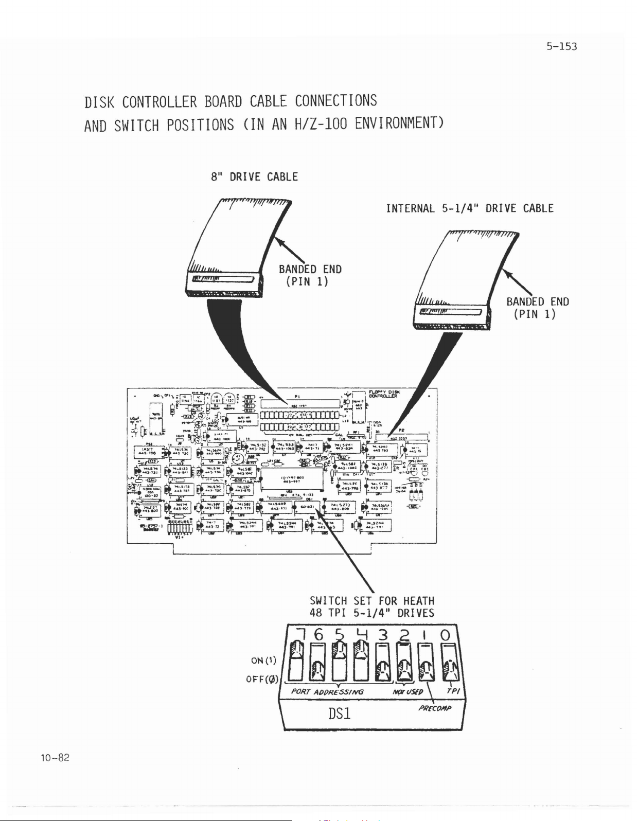
5-153
DISK
AND
SWITCH
CONTROLLER
BOARD
POSITIONS
811DRIVE
CABLE
(IN
AN
CABLE
CONNECTIONS
H/Z-IOO
ENVIRONMENT)
INTERNAL
5-1/411DRIVE
CABLE
10-82
SWITCH
48
fl6~~3210'
O~~~)
.~
~
PORT ADPRESSllt/G
\
-----
SET
FOR
TPI
5-1/411DRIVES
0
~
BB~
DSI
-
HEATH
N(1T
liSE/)
ij
\'
PI?£CMP J
TP/
Page 70
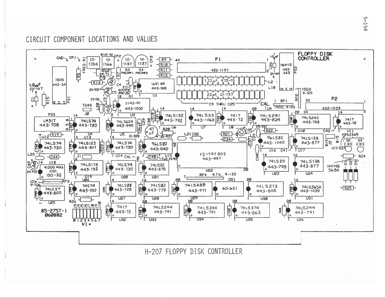
l}1
I
~
l}1
~
CIRCUIT
o
1.0
...
F
2;ro~
COMPONENT
CP
CN),
7805
~42-54
~I~
LOCATIONS
1 - flO'l 10- ,
b
~
~
ij
~-1~Vf
~
~/
25·93'
"''',
PS3
LM~17
442-708
TC43
=
JO
AND
VALUES
r"r2@@~
,,..
'0-
1\37
~9PRE~I
®
~
......J
C4
4~
~
:"0
..,
reO~~
-'
~
,~
i I
SO
411-~
,..,,'"
18
"'3-
443-1000
, -
1
74lS624
443-qqQ
'"
-
...
. 1
10
0 0
1137,
P:ci..2
-D
0
01 \ C9
,
U3
~~
~
-sl@y71R20
~
21-10' - M
~
~
-®D-
~
D
l"Ql
W
443-998
UI
~s~
~
()
<..>
• ,
,
443·'''0
«'='
~==-""'.
74lS32
443-875
o
7",5132
4<3-792
, ,
-r-J-
.»-orr
%L502
0
~I,~~O
-=-,
49
I
OOroJG.
OXDC,.....,,.....,,.....,,.....,,.....,·
0 22pF,
14
74'
443-'''''3
U6 1 U7
l2IC32
= -e::J-
P1
432-1\
" 2
~7~g~~OOOQ}L2+
~WL,JW
Y'-r'Y'-r'Y
nRU
533
~
JOJOOO
2/-757
C25
14
~o
JDi>T1._
-@fr-
35
~F
~o-
= 0
~
'0179'
4<3-'"
0 U22
1 RP4
I,
BO'
'.7k,
,·"3
I OSI
2i:>
20
I
1.0.llF
II~~
"..
_
LIS
~-~150n
/ 1
elf-
20
00
01
~
0
',,,",_
U9 .
74l5:241
443-824
-f.Bggj-
%'5.2
,443-
104
UI6
14
74'520
443-798
0
U23 U24
FLOPPY
~TROLLER
••
,_
10:
7&1'1121$')1
'"
•
9.120
~
C(
RP
1 i I
'-"0
~
0
0'1
33
20
" ,
14lS240
443-7'3
74'S
443-817
0 5b-84
16
I i
DISK
~32-'OS34
C42
'---'lfl
l-...J
~~
"'~417-93'C)
138
IN.,,,
,
o
P2 I
I
I-
7417
J 1
UII
443-72
o
~PS'Z
v
~
...
CBE CBE
-e::J-
2
3(Jl
0
024
~
000
U25
85-2757-1
060882
R2~
-c=J-
('I)
..
lfl
0() !'OO
rTffffffl
Ulllil.lJ
01234567
VI-
0--
lSI
I
..
I 1- ,
..
u
74LS244
443-7ql
U33
H-207
'.
-
2002:9
i I
FLOPPY
DISK
'J:
1:
I 1
{,o-"Z\
~
~
20
0
I
0
1 U30
74LS374
443-803
U35
74LS273
443-805
CONTROLLER
~
74lS3lOSA
443-1039
U31
74LS244
443-791
U36
~
Page 71
ADJUSTMENTS
INTRODUCTION
EQUIPMENT
DATA
SEPARATOR
NEEDED
Frequency Counter
Kit Builder
WRITE
PRECOMPENSATION
Calibration
Method
Circuit
Procedure
Oscilloscope
J2
= 8 < 5 Procedure 5-163
J2
= 8 > 5 Procedure
ADJUSTMENT
Method
ADJUSTMENTS
Board
Method
Method
5-157
5-157
5-157
5-158
5-159
5-160
5-160
5-161
5-162
5-164
-,
, -
- ,
/
Page 72
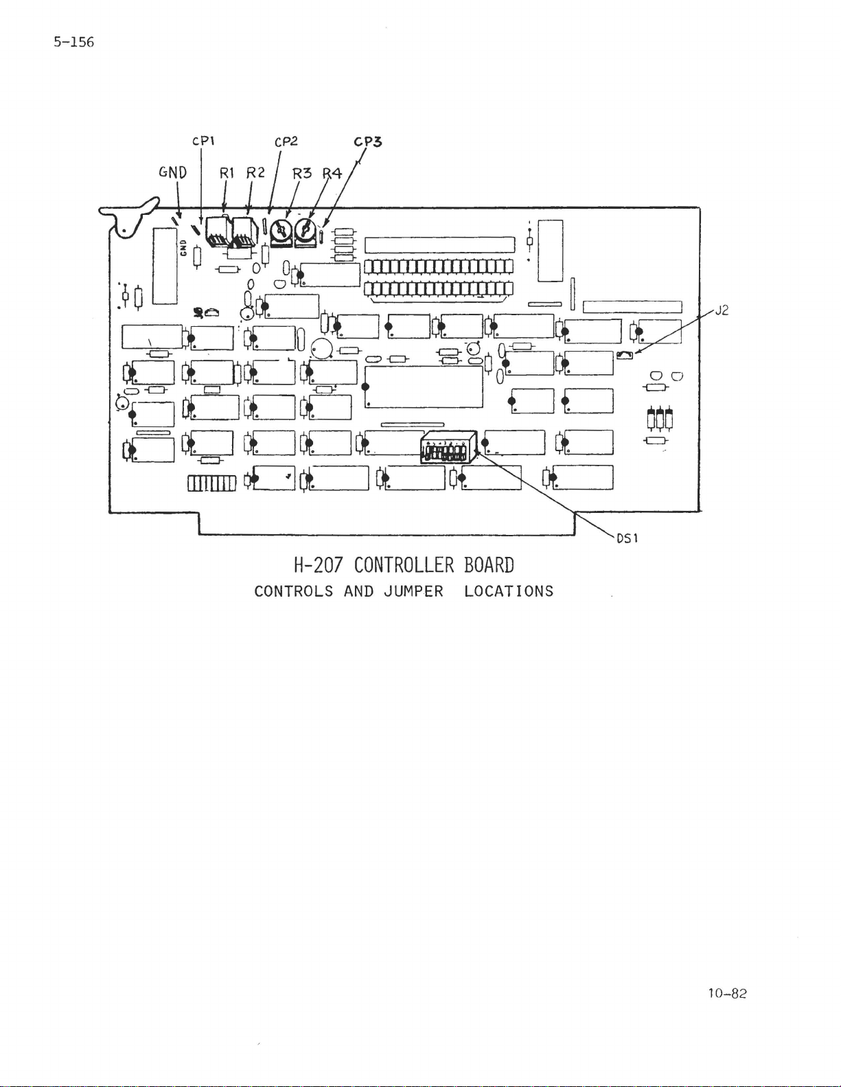
5-156
cPt
CP2
c;.P,3
J2
os,
H-207
CONTROLS
CONTROLLER
AND
JUMPER
BOARD
LOCATIONS
10-82
Page 73

INTRODUCTION
In
this
on how
are
These
Precompensation
to
perform
to
two
are
section
calibrate
adjustments
Data
these
two
of
the
the
Separator
adjustments.
adjustments.
manual,
H-207 Disk
that
the
instructions
Controller
controller
adjustments
Follow
board
the
will
Board.
may
and
procedures
be
given
There
require.
Write
below
5-157
EQUIPMENT
Frequency
Low
Capacitance
Multimeter
Oscilloscope
H-207
DATA
Located
the
method
procedure
H-207.
the
Calibration
SEPARATOR
data
steps
NEEDED
Counter
Probe
on
the
separator.
because
is
the
Locate
in
that
following
the
or
or
or
or
595-2909)
assembly
Board
IM-2420
PKW-105
IM-2202
10-4510
See H-207
(HE
and
ADJUSTMENT
The
of
its
same
procedure.
method
procedure
pages
first
ease
are
procedure
and
given
you
wish
equivalent
equivalent.
equivalent.
equivalent.
assembly
for
details.
two
methods
accuracy.
to
kitbuilders
to
manual
parts
is
use
(optional).
list
to
the
preferred
The
and
adjust
second
of
the
follow
10-82
Page 74

5-158
FREQUENCY
Allow a
top
Remove
Connect
the
controller
Jumper
Connect
Adjust
shows
to
lower
Disconnect
Connect
GND
Connect
CP1
cover
GND
the
+1.40
test
test
fifteen
the
the
test
Locations
the
the
the
COUNTER
minute
of
the
computer
top
cover
common
point
board.
pictorial.
positive
BIAS
ranges
the
point.
point.
control
VDC
(+.05
to
multimeter.
common
test
probe
METHOD
warm-up
in
of
the
test
at
Refer
perform
lead
the
test
volts).
of
of
lead
upper
to
lead
(R2)
the
of
place.
computer.
of
the
left
the
H-207
to
until
Switch
this
the
adjustment
frequency
frequency
the
board
multimeter
side
Controls
the
CP2
the
multimeter
the
with
of
the
test
multimeter
accurately.
counter
counter
the
to
and
point.
display
to
to
the
the
Adjust
display
Disconnect
The
adjustments
Proceed
to
the
shows
WRITE
FREQ
the
control
4.000
to
PRECOMPENSATION
MHz.
frequency
the
Data
(R1)
counter.
Separator
until
ADJUSTMENTS.
the
frequency
are
now
counter
complete.
Page 75

KIT
BUILDER
5-159
METHOD
Remove
Remove
Tack
the
Tack
20
Set
position.
Set
position.
Connect
GND
Reinstall
Connect
and
Adjust
shows
the
accurately.
the
U9,
solder
socket
solder
of
the
the
the
test
apply
the
+1.40
multimeter
controller
U22, and
a
length
for
U9.
wires
socket
PRECMP2control
PRECMP1control
the
common
point.
the
controller
the
positive
power
BIAS
VDC
to
for
to
control
(+.05
to
lower
U30
of
interconnect
U22.
test
test
the
board
from
wire
(R4)
(R3)
lead
board
lead
computer.
(R2)
volts).
ranges
from
their
between
to
to
of
the
into
to
until
You
to
the
computer.
sockets.
pins
pins
a
fully
a
fully
multimeter
the
the
the
will
perform
1 and 20
30,
33,
37,
clockwise
counterclockwise
to
computer.
CP2
test
multimeter
want
this
point
to
switch
adjustment
of
and
the
display
10-82
Allowaperiod
the
R2
Power
Tack
CAL.
Reinstall
computer.
Adjust
of
Power
Remove
Install
Reinstall
The
Proceed
down
solder
+1.40
down
adjustments
to
of
adjustment
the
computer
a
length
the
controller
the
FREQ
VDC
(+0.05
the
computer
all
the temporarily
U9,
U22, and
the
controller
to
WRITE
PRECOMPENSATION
15
again.
control
volts)
the
minutes
and remove
of
wire
board
(R1)
and remove
U30
in
board
Data
for
drifting;
the
between
and
apply
for
a
multimeter
at
test
installed
their
point
the
respective
into
Separator
ADJUSTMENTS.
controller
the
controller
jumper
the
are
then
two
holes
power
display
CP2.
wires.
sockets.
computer.
now
perform
board.
marked
to
the
board.
complete.
Page 76

5-160
WRITE
Located
write
calibration
ki
t.
and
with
preferred
is
included
a
and
PRECOMPENSATION
on
the
precompensation.
circuit
The
second
precompensation
the
controller
method
required.
on
the
particular
follow
the
CALIBRATION
The
calibration
adjust
method,
is
is
drives
JO
out
set
the
and
and
the
the
for
value
that
J2
J2
H-207
5-1/4"
a
are
remain
is
following
method
because
however,
calibration
drive.
steps
in
CIRCUIT
circuit
for
drive
write
used
in
precompensation
for
included
at
the
8 < 5
ADJUSTMENTS
pages
board
requires
data
about
board.
of
when
Locate
that
BOARD
board
use
wi
section
Heath/Zenith
in
the
stock
position
that
are
The
first
is
included
the
use
the
The
its
ease.
precompensation
circuit
the
procedure
procedure.
METHOD
method
thin
the
position.
a
H/Z-100.
of
value
H/Z-100s.
(foil
two
of
drives
first
board
is
the
48
methods
method
an
that
method
The
are
you
primarily
controller
of
TPI,
The
That
bridge).
to
adjust
uses
in
the
oscilloscope
are
is
second
By
120
5-1/4"
values
needed
wish
using
nS.
jumpers
is,
method
to
used
the
H-207
used
the
not
for
use
to
this
board
This
disk
at
JO
is
Youmay
of
precompensation.
from
160nS.
a
customer
not
Method
You
write
precompensation
cal
ibration
when
to
determine
value.
the
that
use
five
mentioned
may
setting
8 > 5
needs
values
200nS,
application
of
WritePrecompensation.
also
precompensation
If
position.
to
the
Gal
ibration
of
precompensation.
240
nS,
above.
use
the
value
board,
precompensation
if
it
is.
be
use
the
you
adjusted
By
installing
and
that
In
calibration
8"
Also
requires
this
for
needed
the
value
will
remember,
instead
circui
280
case,
8"
Oscilloscope
have
nS.
disk
is
for
is
t
circuit
not
8"
greater
to
of
board
DL502,
However,
a
precompensation
proceed
drives.
drives,
jumper
that
R3.
for
you may
These
to
board
obtainable
Method.
than
J2
R4
is
other
being
you
Oscilloscope
Again,
you
so
may
for
with
Remember
will
the
it
the
val
choose
120
setting
if
5-1/4"
control
ues
nS,
have
value
the
the
have
is
in
Page 77

PROCEDURE
5-161
Obtain
HE
595-2909
Connect
a
source
The
positve
source.
Connect
the
GND
Connect
the
CP3
If
not
R4
fully
Set
the
120 nS.
set
the
Turn on
Boot up a
operating
program.
a
calibration
for
the
alligator
of
+5
end
the
black
test
the
yellow
test
already
clockwise.
jumper
If
the
jumper
the
computer.
system
system
construction).
volts
of
any
wire
point
point
on
wire
of
done,
select
drive
to
the
disk.
manual and
circuit
clip
on
the
.1
from
the
from
the
set
R3
wire
requires
desired
Refer
board
of
H-207
uF
glass
the
H-207
the
H-207
fully
of
start
(see
the
calibration
controller
capacitor
calibration
board.
calibration
board.
counterclockwise
the
calibration
more
position.
to
precompensation,
the
appropriate
the
disk
H-207 manual
board
board.
is
a good
board
format
to
board
board
to
to
and
to
10-82
While
H-207
turns
Turn
circuit
This
NOTE:
the
board
on.
off
the
board.
completes
All
diskettes
used.
format
until
computer
write
program
the
precompensation
should
is
LED
and
be
running,
on
disconnect
reformatted
the
adjust
calibration
the
adjustment.
before
R3
on
board
calibration
being
the
just
Page 78

5-162
OSCILLOSCOPE
The
oscilloscope
is
primarily
disk
between
refer
PRECOMP
are
write
beginning
drives.
the
to
the
switch
working
precompensation.
METHOD
used
PRECOMP
table
on.
of
this
method
To
of
points.
TYPEOFORIVE
8"
Double-Density
48
5-1/4".
Doub
5-1/4",
Double-Density
*Precompisbi't 4 in the control latch
X
: Don't
NOTE:
TPI.
1e-
Dens
lty
96
TPI,
Care
Precompisautomatically disabled in single-density operation.
of
to
adjust
understand
switch
below.
DS1
and
Now
perform
section
Precomp
no
N/A
Precomp
JO
Precomp
JO:IN
write
This
JO
Refer
for
tracks
: X
precompensation
the
H-207
the
relationship
setting
table
for
the
the
following
to
the
the
locations
DESIRED
Precomp Precomp
all
Precomp:I1l
JO
: 1
=1
Precomp
JO
Precomp
JO
for
non
of
DS1
shows how
particular
illustration
RESULTS
tracks
*
: X
: 0
• X
: 0
: X
adjustment
Heath/Zenith
that
and
jumper
to
system
steps
to
of
tracks
Precomp·
JO
- X
N/A
Precomp
JO=OUT
the
>43
= 1
exists
set
adjust
at
: 1
JO.
the
you
the
test
Set
the
PRECMP2control
position.
Set
the
PRECMP1control
posi
tion
•
The
position
procedures
precompensation.
write
system.
5-1/4"
is
the
drives
than
procedure
Typical
5-1/4"
8"
precompensation
If
disk
less
than
procedure
where
the
5-1/4"
under
values
disk
disk
drives
drives
of
J2
you
the
drives.
the
under
the
"J2
of
(R4)
(R3)
will
will
Refer
determine
use
to
value
system
5-1/4"
8"
write
= 8 >
or
"J2
write
has
the
8"
write
= 8 <
precompensation
precompensation
5".
precompensation
125
to
200 nS
to
125
175 nS
to
a
fully
to
a
fully
which
when
the
manufacturer's
for
the
only
write
8"
precompensation
precompensation
5".
If
are:
of
adjusting
type
disk
the
typical
typical
clockwise
counterclockwise
the
two
following
write
suggested
of
drives
drives.
in
or
figure
figure,
system
figure
figure,
150
is
nS.
has
greater
use
135 nS
~he
only
use
disk
the
Page 79

J2
= 8 < 5
5-163
PROCEDURE
Connect
Set
50
nS/division
goi
Apply power
If
routine
adjust
displayed
manufacturer's
that
If
drives
5-1/4"
PRECMP2control
on
suggested
If
the
disk
write
routine
adjust
displayed
manufacturer's
for
the
oscilloscope
the
probe
ng
pulse•
to
the
system
on an 8"
the
PRECMP1control
on
type
there
the
drives
that
of
are
in
the
diskette.
oscilloscope
write
system
or
precompensation
on a
the
PRECMP1control
on
drive.
to
Xl0 and
to
display
the
computer.
has
8"
disk
diskette.
the
oscilloscope
suggested
drive.
5-1/4"
system,
only
non
5-1/4"
the
suggested
disk
While
(R4)
corresponds
precompensation
has
Heath/Zenith
adjustment,
diskette.
oscilloscope
probe
set
a 100
drives,
write
drives
start
format
until
Heath/Zenith
write
to
the
While
(R3)
corresponds
the
the
While
(R3)
corresponds
precompensation
GND
and CP3.
oscilloscope
to
300 nS
start
format
until
precompensation
in
addition
format
is
running,
pulse
to
the
for
that
5-1/4"
disk
drives
start
format
until
negative
the
is
the
pulse
to
routine
adjust
width
manufacturer's
type
96 TPI
that
the
format
is
the
pulse
to
at
format
running,
width
the
for
to
8"
disk
on a
the
displayed
of
drive.
require
running,
width
the
value
10-82
Power
Disconnect
This
NOTE:
down
completes
All
diskettes
used.
the
computer.
the
oscilloscope
write
probe.
precompensation
should
be
reformatted
adjustment.
before
being
Page 80

5-164
J2
= 8 > 5
PROCEDURE
Remove
Refer
foil
that
to
the
H-207
Board
Install
Connect
Set
the
50
nS/division
going
the
controller
to
the
connects
8 < 5
Controller
J2
Location
the
floppy
the
oscilloscope
probe
pulse.
H-207 J2
the
position
board
to
X10
to
display
board
location
middle
of
J2.
into
probe
and
set
from
the
a 100
the
pictorial
of
the
the
the
computer.
to
GND
oscilloscope
to
300 nS
computer.
and
J2
position
middle
and CP3.
negative
cut
hole
at
the
of
the
Apply power
While
PRECMP1control
on
suggested
While
PRECMP2control
on
suggested
Power
Disconnect
This
NOTE:
formatting
the
oscilloscope
formatting
the
oscilloscope
down
completes
All
used.
to
write
write
the
the
the
diskettes
the
computer.
a
5-1/4"
(R3)
corresponds
precompensation
an
8"
(R4)
corresponds
precompensation
computer.
oscilloscope
write
should
diskette,
until
diskette,
until
precompensation
be
adjust
the
pulse
with
value.
adjust
the
pulse
with
value.
probe.
reformatted
the
width
the
width
the
adjustment.
displayed
manufacturer's
the
displayed
manufacturer's
before
being
Page 81

TROUBLESHOOTING
INTRODUCTION
EQUIPMENT
H/Z-100
PREWORK
SERVICE
Voltage
Logic
H-207
WAVEFORMS
TEST
HINTS
Level
DISK
NEEDED
FIXTURE
Checks
Checks
CONTROLLER
TEST
5-167
5-167
5-167
5-168
5-169
5-169
5-170
5-171
5-176
·,',::.
/
Page 82

Page 83
INTRODUCTION
To
troubleshoot
section
Located
that
contains
board
techniques,
corrected.
will
after
of
the
in
this
aid
voltages
a
manual
you
hard
most
the
section
in
and
reset.
problems
H-207
in
of
servicing
logic
By
Floppy
conjunction
the
levels
using
can
Disk
manual
the
of
be
Controller,
with
board.
a
normally
standard
quickly
the
schematic.
are
service
The
functioning
troubleshooting
located
use
this
hints
schematic
and
5-167
EQUIPMENT
Frequency
Logic
Low
Multimeter
Oscilloscope
Probe
Capacitance
H/Z-IOO
The
H/Z-100
TPI
disk
boot
is
NEEDED
Counter
TEST
test
drives
defeated
FIXTURE
Probe
fixture
are
(See
IM-2420
IT-471 0
PKW-105
IM-2260
IO-451 0
is
set
the
primary
"Configuration")
up so
boot
.
equival
or
equi
or
equival
or
equivalent.
or
equi
or
that
device.
val
val
the
ent.
ent.
ent.
ent.
5-1/4",
Also,
48
auto
10-82
It
is
operation
a 3
MHz
port
80
assumed
within
or
greater
(Hex),
48
that
TPI,
the
the
H/Z-100.
clock
and
H-207
speed
precompensation
board
That
and
is,
DS1is
is
configured
J1
is
disabled.
jumpered
configured
for
for
for
Page 84

5-168
PREWORK
Once you
for
service,
in
the
power
below
CHECKOUT
Check
•
Polarized
•
01,
•
D1,
• ICs
•
Dirty
•
Solder
• Cold
have
procedure
is
applied
may
have
PROCEDURE
the
H-207
Q2,
D2,
installed
S-100
bridges.
solder
received
use
already
capacitors
or
03
or
D3
board
joints.
the
checkout
are
problems
to
the
been
Controller
installed
installed
backwards.'
contacts.
a
H-207
circuit
implemented
Board
installed
incorrectly.
backwards.
Floppy
procedure
that
may
board.
for:
backwards.
Controller
below.
be
identified
Many
in
your
Board
Included
before
of
the
checks
preworking.
in
•
Resistor
•
Correct
•
Switch
•
Correct
7805
78M12
LM317
After
H/Z-l00
If
controller
Adjustments
If
the
the
making
test
board
problem
packs
jumpering.
settings
voltage
at
PS1.
at
PS2.
at
PS3.
these
fixture
appears
board
section
still
installed
of
OS1.
regulator
checks,
and
using
of
this
exists,
backwards.
for
install
confirm
to
operate
the
procedure
manual.
proceed
location:
the
customer's
properly,
to
the
H-207
in
the
Service
into
complaint.
align
Alignment
Hints.
your
the
and
Page 85

5-169
-t!>
SERVICE
VOLTAGE
Wi
th
following
test
the
are
•
•
•
•
VDC
+5VDC
HINTS
CHECKS
the
H-201
voltage
point
mul
timeter.
disconnected
The
voltage
The
voltage
The
voltage
The
voltage
+1.40
is
installed
a
good
fram
at
PS
at
PS2-12
at
PS3-5
at
CP2
VDC
checks
It
is
the
1-5
is
place
assumed
controller
is
+5
is
is
+5
+1.40
in
with
+12
your
to
VDC.
VDC.
VDC.
VDC.
test
your
connect
that
board.
PI
fixture,
multimeter.
the
cammon
the
disk
+12VDC
perform
drive
the
The
GND
lead
FLa>PY DISK
CONTROl.1.£R
of
cables
10-82
If
the
values
voltage
problem
Level
Alignment
voltages
stated,
regulators
still
Checks
and
at
these
it
can
are
exists,
and
Waveforms.
Adjustments.
test
be
safely
operating
further
points
aid
Otherwise,
are
assumed
properly.
can
within
U1, U5,
be
found
proceed
5%
of
and
Assuming
in
to
the
the
the
Logic
the
Page 86
5-170
LOGIC
On
H-207
test
(*).
each
for
with
Continue
test
previous
Before
lead
procedure
It
foil
As
press
indicates
"Read
of
logic
Completed"
LEVEL
the
following
board.
the
If
IC
these
the
an
you
ing
doesn't
runs,
you make
RETURN.
Completed"
a
(P)
probe)'
CHECKS
ICs
in
you
don't
listed
ICs
asterisks.
tracing
IC
that
IC
that
replace
up
to
gives
cover
or
open
the
that
indication,
interval.
pages
When
are
it.
will
performing
the
left
get
immediately
listed
backwards
matches
you
tested
the
You
only
the
the
such
resistors.
following
Logic
probe
is
printed
momentarily
is
column
the
suggested
in
the
is
suspected
must
most
things
checks,
states
pulses
the
pulse
a
logic
the
to
the
the
using
suggested
likely
do
likely
as
located
on
probe
tests,
indicated
logic
right.
left
this
the
IC,
this
causes
open ground
press
one
the
rate
change
state,
column
procedure
logic
bad
check
because
the
inside
or
more
screen.
(as
during
analysis
you need
by
an
then
The
logic
below
state.
IC.
the
other
this
to
the
foils,
(B)oot
parenthesis
times
In
indicated
the
of
only
asterisk
check
states
the
until
lines
checkout
problem.
shorted
key and
while
the
case
by
"Read
the
to
ICs
you
The
the
The
schematic
has
been
troubleshooting
To
setup
one
48
computer.
performed.
the
TPI,
shows
areas
H-207
5-114"
for
the
not
disk
logic
Refer
covered
the
states
to
in
following
drive
these
the
test.
to
after
logic
following
connect
P1
and
a
CTRL/RESET
states
tests.
at
turn
on
for
least
the
Page 87

5-171
H-207
CHECK
*Q3
Collector
*U
1-16
*U7-4
*U9-19
*U10-12
*U10-14
*U10-16
,
*U
11-4
*U
11-6
*U
11-8
*U
11-10
*U
11-12
DISK
= 2
MHz
= L
=L
H
=
H
=
H
=
H
=
H
=
H
=
L
=
H
=
CONTROLLER
TEST
IF
=Z
U21-8
U13-6
U7-5
CTR/RESET. U7-4
remain
If
U30
U10
U10
U10
U11-3
11-5
U
U11-9
U11-11
U11-13
NOT
(Also
not,
or
or
or
or
OKAY,
press
low
then
the
data
U22
is
U22
is
U22
is
CHECK
for
about
replace
bus
defective.
defective.
defective.
and
should
release
18
U15.)
is
defective.
seconds.
*U22-2
*U22-3
*U22-23
*U22-24
*U22-27
*U22-34
*U22-35
*U22-36
*U
31-1
*U
31-15
*U32-6
*U35-11
*U36-1
*U36-19
End
of
=
=
=
=
=
=
=
=
=
=
=
=
=
=
test.
(H)
(H)
(H)
1
P
L
L
H
(H)
(H)
(H)
(p)
(H)
(H)
MHz
U21-11
U21-3
U15-7
U13-8
U16-9
U9
is
U9
is
U9
is
U27-8
U17-14
U32-5
U28-4
U27-8
U27-8
defective.
defective.
de
fective.
10-82
Page 88

5-172
U4-3
U4-5
U4-9
U4-11
U4-12
U5-8
U7-5
U7-11
U7-12
U7-13
U
10-3
U10-17
U11-3
U11-5
U
11-9
U11-11=L
U11-13
U12-3
U12-5
U12-9
U12-11
= 4
= 2
=L
= P
=L
= 4
= H
=L
= L
= H
= L
= H
= H
= H
= H
= H
= 4
= 2
= 1
=2
MHz
MHz
MHz
MHz
MHz
MHz
MHz
U5-8
U4-3
U4-11.
U4-5
U30
or
U5
or
U1
incorrectly
U23-8
U30
or
U30
or
U7-11.
UlO-17
U33-9
U16-7
U24-14
U24-12
U24-15
U24-13
U18
is
U12-3
U12-11
U12-5
U4-12
the
data
defective;
the
data
the
data
U7-12
bad.
bus
adjusted.
bus
bus
is
defective.
R1
or
is
defective.
is
defective.
R2
U
13-4
U13-5
U13-6
U13-8
U13-9
U
13-10
U
14-8
U14-11
U14-12
U15-4
U15-7
U
16-4
U16-7
U16-9
U
16-11
=L .
= 2
= 2
= 1
= 1
L
=
=L
=
1
H
=
= H
=
(H)
= L
= H
= P
= P
MHz
MHz
MHz
MHz
MHz
U4-9
U4-5
U13-4.
U13-9.
U12-9
U14-8
U14-11,
U12-9
U7-13
U22
or
U
15-4
U1
or
U16-4
U16-11
U9
is
U13-5
U13-10
U14-12
the
data
U22
is
defective.
bus
defective.
is
defective.
Page 89
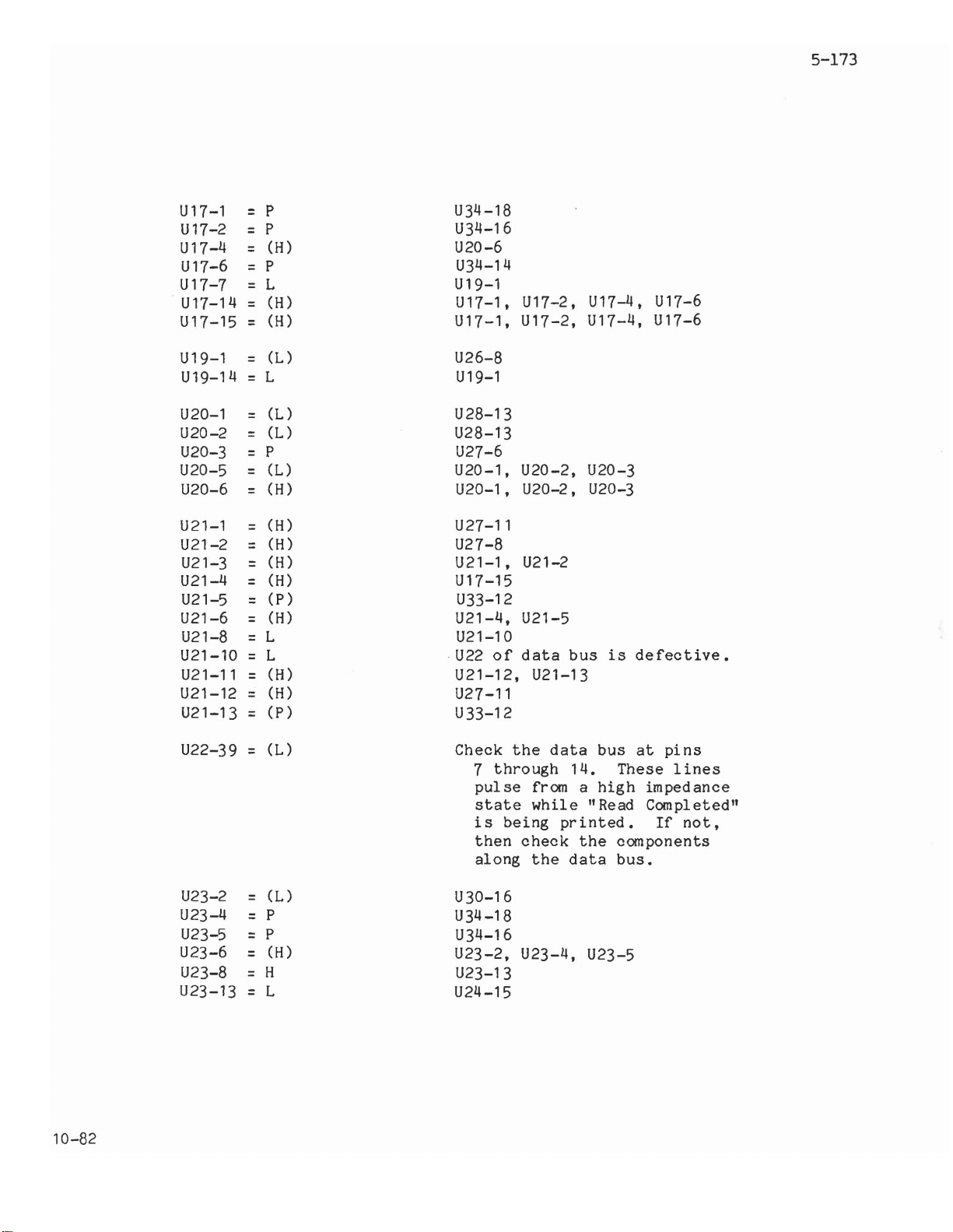
5-173
U
17-1
U17-2
U17-4
U17-6
U17-7
U17-14
U17-15
U19-1
U19-14
U20-1
U20-2
U20-3
U20-5
U20-6
U21-1
U21-2
U21-3
U21-4
U21-5
U21-6
U21-8
U21-1O
U21-11
U21-12
U21-13
P
=
P
=
(H)
=
P
=
L
=
(H)
=
(H)
=
(L)
=
L U19-1
=
(L)
=
(L)
=
P
=
(L)
=
(H)
=
(H)
=
(H)
=
(H)
=
(H)
=
(P)
=
(H)
=
L
=
L
=
(H)
=
(H)
=
(P)
=
U34-18
U34-16
U20-6
U34-14
U19-1
of
U17-2,
U17-2,
U20-2,
U21-2
U21-5
data
U21-13
U
17-1,
U17-1,
U26-8
U28-13
U28-13
U27-6
U20-1, U20-2,
U20-1,
U27-11
U27-8
U21-1,
U17-15
U33-12
U21-4,
U21-10
U22
U21-12,
U27-11
U
33-12
bus
U17-4,
U17-4,
U20-3
U20-3
is
U17-6
U17-6
defective.
10-82
U22-39
U23-2
U23-4
U23-5
U23-6
U23-8
U23-13
=
=
=
=
=
=
=
(L)
(L)
P
P
(H)
H
L
Check
U30-16
U34-18
U34-16
U23-2, U23-4,
U23-13
U24-15
7
through
pul
state
is
then
along
the
se
being
check
data
from
while"
the
bus
14.
a
high
Read
printed.
the
data
U23-5
at
pins
These
components
bus.
lines
impedance
Completed"
If
not,
Page 90

5-174
U24-1
U24-2
U24-3
U24-6
U24-12
U24-13
U24-14
U24-15
U25-1
U25-2
U25-3
U25-4
U25-5
U25-6
U25-12
U25-13
U26-2
U26-3
U26-4
U26-5
U26-8
U26-10
U26-11
U26-12
= L
L
=
L U30
=
H
=
H
=
H
=
H
=
L
=
L
=
L
=
L
=
(L)
=
L
=
(H)
=
(H)
=
(L)
=
(H)
=
(L)
=
(H)
=
(H)
=
(L)
=
(H)
=
(L)
=
(H)
=
the
U30
or
U30
or
or
U30
or
U24-1.
U24-1.
U24-1. U24-2.
U24-1. U24-2.
U19-7
U10-3
U
10-3
U22-39
U19-14
U25-3.
U25-1.
U22-39
U23-6
U20-5
U25-12
U26-2.
U26-10.
U25-6
U20-5
U23-6
data
the
data
the
data
the
data
U24-2.
U24-2.
U25-4.
U25-2.
U26-3.
U26-11.
bus
bus
bus
bus
U24-3.
U24-3.
U24-3.
U24-3.
U25-5
U25-13
U26-4
U26-12
is
defective.
is
defective.
is
defective.
is
defective.
U24-6
U24-6
U24-6
U24-6
U27-1
U27-3
U27-4
U27-5
U27-6
U27-8
U27-9
U27-10
U27-11
U27-12
U27-13
U28-1
U28-2
U28-3
U28-4
(L)
=
(H)
=
P
=
P
=
P
=
(H)
=
p
=
(L)
=
(H)
=
(L)
=
(H)
=
(H)
=
(L)
=
(L)
=
(P)
=
U22-39
U27-1
U33
defective.
U33
defective.
U27-5.
U27-9.
U33
defective.
U20-5
U27-12.
U28-10
U26-5
U28-2.
U33
defective.
U33
defective.
U28-6
U27-4
U27-10
U27-13
U28-3
Page 91

5-175
U28-6
U28-8
U28-9
U28-10
U28-11
U28-12
U28-13
U29-19
U30-1
U30-11
U30-16
U32-5
U33-9
U33-12
U34-14
U34-16
U34-18
=
=
=
=
=
=
=
=
=
=
=
=
=
=
=
=
=
(p)
(H)
p
(L)
(p)
(H)
(L)
(p)
H
(H)
(L)
(H)
H
(p)
P
P
P
U33-12
U20-6
U34-14
U28-8,
U29-19
U28-1
U28-11,
U29,
U33-9
U21-6
U30-1,
problem
U27-3
U33
defective.
U33
defective.
defective.
U34
defective.
U34
defective.
U34
U28-9
U34,
U30-11.
U28-12
or
•
OSl
or
defective.
data
bus
10-82
Page 92

5-176
WAVEFORMS
The
waveforms
functioning
wav
eforms
you
are
servicing.
as
shown
controller
a
reference
in
this
section
board
when
in
checki
are
generated
an
idle
ng waveforms on
state.
by a
normally
Use
the
these
board
The waveform
was
taken
This
that
frequency
around
is
originates
In an
The
waveform
was
taken
This
that
oscillator
frequency
is
1
in
an
The waveform
was
taken
is
the
originates
U5-8. The
this
the
board
state.
from
the
idle
of
250 kHz.
from U22-24.
is
the
originates
of
MHz
when
idle
VCO
signal
at
.the
U22-26.
RCLK
signal
at
state
circuits.
state.
from CP1.
signal
from
frequency
is
RCLK
at
CLK
this
the
at
is
in
the
the
signal
from
the
the
4
MHz
an
right
U1-12.
is
right
the
signal
board
right
This
that
VCO,
of
when
idle
The
is
2V/DIV
I-
.......
--_._-
2V/DIV
r
~
ZV/DtV
I-~'-~-""-'
...
t---
~
..
or
--..
-
._
U
..
_....
..._.....
to
•
._._
.....
.:.-t
.
..
-
--
..
-
•.
g'
-+--+-
...
_.-
500nS/DIV
1--
~
.J
- II
fOOn5/DIV
2,uS/D11J
1
.1
'r-j
n-
ttl+
_.k
""=-
1--
t--
Page 93

PARTS
LISTS
DISK
CONTROLLER
CALIBRATION
CIRCUIT
CIRCUIT
BOARD
BOARD
5-179
5-180
/
Page 94

Page 95

PARTS
Lbr
CIRCUIT
Cornp.
'10.
DISK
CAPACITORS
Cl
C2
C3
CII
C5
C6
C7
C8
C9
C
10
Cll
C12
C13
C14
C15
C16
C17
C18
C19
C20
C21
C22
C23
C211
C25
C26
C27
C28
C29
C30
C31
C32
C32a
C33
C34
C35
C36
C37
C38
C39
C40
Clll .1ufoarell0
CII2
CII3
C44
CII5
-"
0
I
(Xl
I'\)
DESCRIPTION
CONTROLLER
1.0uftantalllll
none
.47ufpolycarbonate
10uftantalllll
10uftantalllll
10uftantalllll
.1ufcer8lll1c
.1ufcer8lllic
22pfceramic
22pfceramic
22pfcer8lll1c
22pfcer1lll1c
22pfceram1c
22pfcerllllic
22pfceramlc
22pfceraal0
22pfceralc
22pfceram1c
22pfceram1c
22pfcer8lll1c
22pfceram1c
22pfceram1c
22pfceraa1c
22pfcer8lll10
22pfceraa1c
1.0uftantalllll
.1
.uf
ceraa
.1ufceram1c
36pfcer8lll1c
47ufelectrolytlc
.1ufcer8lll1c
• 1ufceram1c
10uftantalllll
.1ufceraalc
.1ufceramic
10uftantalllll
.1ufoeram1c
.1ufcer8lll1c
180pfcerlllllc
180pfcerlllllc
.1ufcerlllll0
.1ufoerllll10
.1ufceramic
.1ufceramic
.1ufcer8lllic
lc
CIRCUIT
HEATH
Part
HE
25-197
HE
29-71
HE
25-220
HE
25-220
HE
25-220
HE
21-762
HE
21-762
HE
21-757
HE
21-757
HE
21-757
HE
21-757
HE
21-757
HE
21-757
HE
21-757
HE
21-757
lIE
21-757
HE
21-757
HE
21-757
HE
21-757
HE
21-757
lIE
21-757
HE
21-757
HE
21-757
HE
21-757
HE
25-197
HE
21-762
HE
21-762
HE
21-709
HE
25-921
HE
21-762
HE
21-762
HE
25-220
HE
21-762
lIE
21-762
HE
25-220
lIE
21-762
lIE
21-762
HE
21-746
HE
21-7116
HE
21-762
HE
21-762
HE
21-762
HE
21-762
HE
21-762
HE
21-762
No.
BOARD
CIRCUIT
Compo
CAPACITORS
CII6
C47
C48
CII9
C50
C51
C52
C53
C54
C55
C56
C57
C58
C59
C60
C61
C62
C63
INDUCTORS
Ll
L2
L3
L4
L5
L6
L7
L8
L9
Ll0
Lll
L12 1, 22uHbead
L13
Ll11
L15
L16
L17
L18
L19
L20
L21
L22
L23
DESCRIPTION
No.
(CONTINUED)
.1ufcer8lll1c
.1ufceran1c
1.0uftantal
10uftantalllll
.1ufcerllllic
.1ufceraic
.1ufceraic
.1ufcer8lll1c
.1ufcer8lll1c
.1ufcer8lll1c
.1ufcera1c
.1ufceram1c
.1ufceram1c
.1ufcerllll10
.1ufceralc
.•1uf
.1ufcerlllllc
.1ufceram1c
35
1,22uHbead
1.22uHbead
1.22uHbead
1.22uHbead
1.22uH
1,22uHbead
1,22uHbead
1.22uHbead
1.22uHbead
1.22uH
1.22uHbead
1.22uHbead
1.22uHbead
1.22uHbead
1.22uHbead
1.22uHbead
35
35
35
35
35
uH
uH
uH
uH
uH
uH
ceraa10
bead
bead
um
HEATH
Part
HE
21-762
HE
21-762
HE
25-197
HE
25-220
HE
21-762
HE
21-762
HE
21-762
HE
21-762
HE
21-762
HE
21-762
HE
21-762
HE
21-762
HE
21-762
HE
21-762
HE
21-762
HE
21-762
HE
21-762
HE
21-762
HE
235-229
HE
475-15
lIE
1175-15
HE
475-15
lIE
475-15
HE
1175-15
lIE
1175-15
HE
475-15
lIE
475-15
lIE
475-15
HE
1175-15
HE
475-15
HE
1175-15
HE
475-15
HE
1175-15
lIE
1175-15
HE
1175-15
lIE
475-15
HE
235-229
HE
235-229
lIE
235-229
HE
235-229
HE
235-229
No.
I
I I
CiRCUIT
Cornp.
RESISTORS
Rl
R2
R3
RII
R5
R6
R7
R8
R9
RIO
Rll
R12
R13
RIll
R15
R16
R17
R18
R19
R20
R21
R22
R23
R211
R25
R26
RES
RPI 150
RP2
RP3
RP4
I
'10.
ISTOR
DESCRIPTION
10
k1lohm
100
kilohm
2
kilohm
kilohm
ohm
kilohm
ohm
ohm
ohm
kilohm
ohm
kilohm
ohm
ohm
ohm
kllohm
ohm
ohm
ohm
ohm
kilohm
kilohm
control
control
2
47
none
47
JlIIlper
1 mel0hm
1000
3900
1800
117
JlIIlper
720
none
none
120
237
1 lIelohlll
3900
2200
1000 olD
120
1000
1000
PACKS
150
10
4.7
control
control
1/4
1/11
1/11
1/11
1/4
1/4
1/11
1/11
1/11
1/4
1/4
1/4
1/11
1/11
1/11
1/4
1/11
watt.
watt,
watt,
watt,
watt.
watt.
watt,
watt,
watt,
watt,
watt,
watt,
watt,
watt.
watt.
watt,
watt,
HEATH
Part
No.
HE
10-1154
HE
10-1180
HE
10-1137
HE
5S
5S
5S
5S
5S
5S
5S
IS
5S
1S
5S
IS
1S
5S
5S
5S
5S
10-1137
HE
6-1170-12
HE
6-1173-12
HE
6-105-12
HE
6-102-12
HE
6-392-12
HE
6-182-12
HE
6-1173-12
HE
6-7200-12
HE
6-124-12
HE
6-2370-12
lIE
6-105-12
HE
6-3901-12
HE
6-2201-12
HE
6-102-12
lIE
6-1211-12
HE
6-102-12
HE
6-102-12
HE
9-120
HE
9-120
HE
9-106
HE
9-133
U'I
-...]
1.0
I
~
Page 96

PARTS
CIRCUIT
Compo
LIST
No.
DESCRIPTION
HEATH
Part
No.
CIRCUIT
Compo
No.
DESCRIPTION
HEATH
Part
No.
CIRCUIT
Compo
No.
DESCRIPTION
HEATH
Part
No.
U1
I-'
(Xl
o
I
CONTROLLER
DISK
(
CONTINUED)
INTEGRATED
PSI
PS2
PS3
Ul
U2
U3
U4
U5
U6
U7
U8
U9
Ul0 745240
Ul1
U12
U13
U14
U15
U16
U17
U18
U19
U20
U21
U22
U23
U24
U25
U26
Un
U28
U29
U30
U31
U32
U33
U34
U35
U36
CIRCUITS
78055Vregul
78M12
1Jl317
WD1691
none
2143-01
74LS74
74LS624
74LS 132
74LS33
7417
74LS241
7417
74LS74
74LS125
74LS74
96LS02
96LS02
74LS
4.000
74LS175
74LS74
74LS32
FD1797B02
74LS20
74LS
74LS27
74S74
74LSOO
74LS02
74LS688
74LS273
74LS365A
7417
74LS244
74LS244
74LS374
74LS244
138
138
+12V
+adj
MHz
CIRCUIT
ator
regulator
regulator
oao111ator
BOARD
OTHER
HE
442-54
HE
442-663
HE
442-708
HE
443-998
HE
443-1000
HE
443-730
HE
443-999
HE
443-792
HE
443-1063'
HE
443-72
HE
443-824
HE
443-753
HE
443-72
HE
443-730
HE
443-811
HE
443-730
HE
443-1040
HE
443-1040
HE
443-877
HE
150-132
HE
443-752
HE
443-730
HE
443-875
HE
443-997
HE
443-798
HE
443-877
HE
443-800
HE
443-900
HE
443-728
HE
443-779
HE
443-971 Heat
HE
443-805
HE
443-1039
HE
443-72
HE
443-791
HE
443-791
HE
443-863
HE
443-191
I
.
Dl
D2
D3
1:61
Ql
Q2
Q3
CONNECTORS-SOCKETS
P2
PI
HARD/ARE
MISCELLANEOUS
CIRCUIT
CCflPONENTS
lN4148
lN4148
lN4148
8-seotion
TIS74
HPS2369
HPS2369
I-pin
8-pin
14-pinICsooket
16-pinICsooket
18-pinICsooket
20-pin
40-pinICsooket
34-pin
oonneotor
50-pin
oonneotor
'4
lookwasher
4-40
4-40x5/16"
H-207
PC
board
S11ioone
S-100
extraotor
Wire,
Wire,
diode
diode
diode
slide
transistor
transistor
transistor
oonneotor
inlineICsocket
IC'
right-angle
right-angle
nut
sink
manual
oirouit
solid
white
sWitoh
socket
sorew
grease
board
solid
HE
HE
HE
HE
HE
HE
HE
HE
HE
HE
HE
HE
HE
HE
HE
HE
HE
HE
HE
HE
HE
HE
HE
HE
HE
HE
56-84
56-84
56-84
60-621
417-246
417-937
417-937
423-121
434-230
434-298
434-299
434-310
434-311
434-253
432-1053
432-1197
595-2909
254-9
252-2
250-213
215-669
85-2757-2
352-13
266-1203
340-8
344-59
CALIBRATION
R501
R502
C501
DL501
0501
U501
U502
10
k11ol'l1l
330
.1uFoeramio
Delay
Alligator
PC
board
Alligator
Wire,
Wire,
Wire,
LST5053
l-pin
14-p1nICsooket
74LSOO
14LS14
ohm
line
blaok
red
white
LED
sooket
1/4
1/4
olip
olip
stranded
CIRCUIT
watt,
51
watt,
51
insulator
stranded
stranded
BOARD
HE
6-103-12
HE
6-331-12
HE
21-162
HE
41-10
HE
73-34
HE
85-2800-1
HE
260-16
HE
344-90
HE
344-92
HE
344-94
HE
412-640
HE
432-120
HE
434-298
HE
443-728
HE
443-730
Page 97

CIRCUIT
BOARD
X-RAY
VIEW
------------
Page 98

 Loading...