

查询ZL49010供应商
ZL49010/1, ZL49020/1, ZL49030/1
Wide Dynamic Range DTMF Receiver
Data Sheet
Features
• Wide dynamic range (50dB) DTMF Receiver
• Call progress (CP) detection via cadence
indication
• 4-bit synchronous serial data output
• Software controlled guard time for ZL490x0
• Internal guard time circuitry for ZL490x1
• Powerdown option (ZL4901x & ZL4903x)
• 3.579MHz crystal or ceramic resonator (ZL4903x
and ZL4902x)
• External clock input (ZL4901x)
• Guarantees non-detection of spurious tones
Applications
• Integrated telephone answering machine
• End-to-end signalling
• Fax Machines
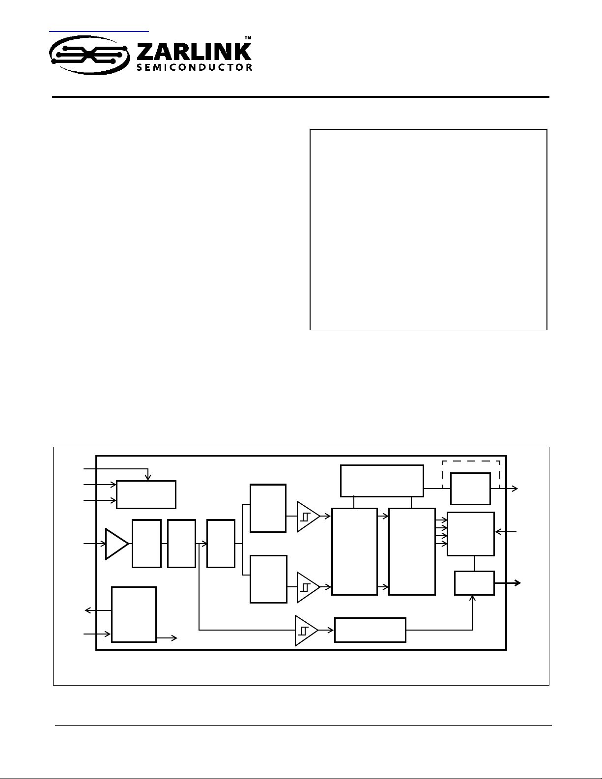
Description
The ZL490xx is a family of high performance DTMF
receivers which decode all 16 tone pairs into a 4-bit
binary code. Th ese devices incorporate an AGC for
wide dynamic range and are suitable for end-to-end
signalling. The ZL490x0 provides an early steering
(ESt) logic output to indicate the detection of a DTM F
September 2003
Ordering Information
ZL49010DAA 8 Pin PDIP Tubes
ZL49011DAA 8 Pin PDIP Tubes
ZL49020DAA 8 Pin PDIP Tubes
ZL49021DAA 8 Pin PDIP Tubes
ZL49030DCA 1 8 P i n SOIC Tubes
ZL49030DCB 18 Pin SOIC Tape & Reel
ZL49030DDA 20 Pin SSOP Tubes
ZL49030DDB 20 Pin SSOP Tape & Reel
ZL49031DCA 18 Pin SOIC Tubes
ZL49031DCB 18 Pin SOIC Tape & Reel
ZL49031DDA 20 Pin SSOP Tubes
ZL49031DDB 20 Pin SSOP Tape & Reel
-40°C to +85°C
signal and requires external software guard time to
validate the DTMF digit. The ZL490x1, with preset
internal guard times, uses a delay steering (DStD)
logic output to i ndicate the detection o f a valid DTMF
digit. The 4-bit DTMF binary digit can be clocked out
synchronously at th e serial data (SD) outpu t. The SD
pin is multiplexed with call progress detector output. In
the presence of supervis ory tones, the call progress
1
PWDN
VDD
VSS
2
OSC2
OSC1
(CLK)
1. ZL49010/1 and ZL49030 /1 only.
2. ZL49020/1 and ZL49030 /1 only.
3. ZL490x1 only.
Voltage
Bias Circuit
AGC
Oscillator
and
Clock
Circuit
Zarlink, ZL and the Zarlink Semiconductor logo are trademarks of Zarlink Semiconductor Inc.
Steering
Circuit
High
Group
Filter
Antialias
Filter
To All Chip Clock s
Dial
Tone
Filter
Digital
Detector
Algorithm
Low
Group
Filter
Energy
Detection
Figure 1 - Functional Block Diagram
1
Zarlink Semiconductor Inc.
Copyright 2003, Zarlink Semiconductor Inc. All Rights Reserved.
Code
Converter
and
Latch
Digital
Guard
3
Time
Parallel to
Serial
Converter
& Latch
Mux
ESt
or
DStD
ACK
SD
ZL49010/1, ZL49020/1, ZL49030/1 Data Sheet
detector circuit indicates the cadence (i.e., envelope) of the tone burst. The cadence information can then be
processed by an extern al microcont roller to identi fy specific c all progress s ignals. The ZL49 02x and ZL490 3x can
be used with a crystal or a cera mic resona tor without additional componen ts. A power-down op tion is prov ided for
the ZL4901x and ZL4903x.
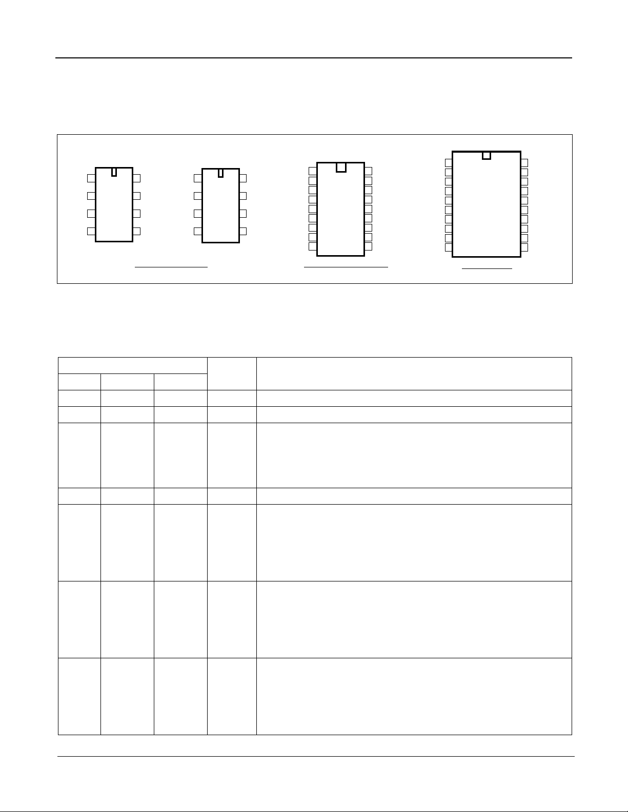
NC
NC
NC
NC
NC
ZL49030/1
1
2
3
4
5
6
7
8
9
10
20 PIN SSOP
20
19
18
17
16
15
14
13
12
11
ZL49010/1 ZL49020/1 ZL49030/1
INPUT
PWDN
CLK
VSS
1
8
2
7
3
6
4
5
8 PIN PLASTIC DIP
VDD
ESt/
DStD
ACK
SD
INPUT
OSC2
OSC1
VSS
1
2
3
4
VDD
8
ESt/
7
DStD
ACK
6
SD
5
INPUT
PWDN
OSC2
OSC1
VSS
1
NC
2
3
4
5
NC
6
NC
7
NC
8
9
18 PIN PLASTIC SOIC
18
17
16
15
14
13
12
11
10
VDD
NC
NC
ESt/DStD
NC
ACK
NC
SD
NC
INPUT
PWDN
OSC2
OSC1
VSS
Figure 2 - Pin C onnectio ns
Pin Description
Pin #
4903x 4902x 4901x
21 1INPUTDTMF/CP Input. Input signal must be AC coupled via capacitor.
42 -OSC2Oscillator Output.
63 3OSC1
94 4V
11 5 5 SD Serial Data/Call Progress Output. This pin serves the dual function
13 6 6 ACK Acknowledge Pulse Input. After ESt or DStD is high, applying a
15 7 7 ESt
Name Description
Oscillator/Clock Input. This pin can either be driven by:
(CLK)
1) an external digital clock with defined input logic levels. OSC2
should be left open.
2) connecting a crystal or ceramic resonator between OSC1 and
OSC2 pins.
Ground. (0V)
SS
of being the serial data output when clock pulses are applied after
validation of DTMF signal, and also indicates the cadence of call
progress input. As DTMF signal lies in the same frequency band as
call progress signal, this pin may toggle for DTMF input. The SD pin
is at logic low in powerdown state.
sequence of four pulses on this pin will then shift out four bits on the
SD pin, representing the decoded DTMF digit. The rising edge of the
first clock is used to latch the 4-bit data prior to shifting. This pin is
pulled down internally. The idle state of the ACK signal should be
low.
Early Steering Output. A logic high on ESt indicates that a DTMF
(ZL490x0)
signal is present. ESt is at logic low in powerdown state.
NC
NC
VDD
NC
ESt/DStD
NC
ACK
SD
NC
NC
DStD
(ZL490x1)
Delayed Steering Output. A logic high on DStD indicates that a
valid DTMF digit has been detected. DStD is at logic low in
powerdown state.
2
Zarlink Semiconductor Inc.
ZL49010/1, ZL49020/1, ZL49030/1 Data Sheet
Pin Description (continued)
Pin #
Name Description
4903x 4902x 4901x
18 8 8 V
Positive Power Supply (5 V Typ.) Performance of the device can be
DD
optimized by minimizing noise on the supply rails. Decoupling
and VSS are therefore recommended.
DD
1,5,7,8,
capacitor s across V
--NCNo Connection. Pin is unconnected internally.
10, 12,
14,16,
17
3- 2PWDNPower Down Input. A logic high on this pin will power down the
device to reduce power consumption. This pin is pulled down
internally and can be left open if not used. ACK pin should be at logic
’0’ to power down device.
Device
Type
8 Pin 18 Pin 20 Pin PWDN
2 Pin
OSC
Ext
CLK
ESt DStD
ZL49010 x x x x
ZL49011 x x x x
ZL49020 x x x x
ZL49021 x x x x
ZL49030 x x x x x x
ZL49031 x x x x x x
Table 1 - Summary of ZL490 x0/1 Produc t Fa mi ly
Functional Descripti on
The ZL490xxs are high performance and low power consumption DT MF receivers. These devices provide wide
dynamic range DTMF detection and a serial decoded data output. These devices also incorporate an energy
detection circuit. An inp ut voiceband sig nal is applied to the dev ices via a series decoupling ca pacitor. Following
the unity gain buffering, the s ign al ent ers the AGC circuit fo ll owed by an anti-aliasing fi lter. The bandlim ite d o utpu t
is routed to a di al to ne fil ter stage and to th e inp ut of the ene rgy detectio n circuit. A b andsp lit fi lter is the n use d to
separate the input DTM F signal into high and low gro up tones. The high group and low group tones are then
verified and deco ded by the internal frequency countin g and DTMF detection circuitry. Following the detectio n
stage, the valid DTMF digit is translated to a 4-bit binary code (via an internal look-up ROM). Data bits can then be
shifted out serially by applying external clock pulses.
Automatic Gain Control (AGC) Circuit
As the device operates on a sing le pow er supp ly, the input signal is biased int ernal ly at appr ox imately VDD/2. With
large input signal amplitude (between 0 and approximately -30dBm for each tone of the composite signal), the AGC
is activated to preve nt the input signal from bein g clipped. At low input level , the AGC remains inactive a nd the
input signal is passed directly to the hardware DTMF detection algorithm and to the energy detection circuit.
Filter and Decoder Section
The signal entering the DTMF detection circuitry is filtered by a notch filter at 350 and 440 Hz for dial tone rejection.
The composite dual- tone signal is further split into its in dividual high and low frequency compon ents by two 6
order switched capaci tor bandpass filters. The high group and low group tones are the n smoothed by separate
th
3
Zarlink Semiconductor Inc.

ZL49010/1, ZL49020/1, ZL49030/1 Data Sheet
output filters and sq uared by high gain limiting c omparators. The resulting squa rewave signals are applie d to a
digital detection circuit where an averaging algorithm is employed to determine the valid DTMF signal. For
ZL490x0, upon recogni tion of a valid frequen cy from each tone group, the early st eering (ESt) output will go high ,
indicating that a DT MF tone has been detected . A ny s ubs eq uen t l oss of DT M F s ig nal c on diti on wi ll c au se th e ESt
pin to go low. For ZL490x1, an internal delayed steering counter validates the early steering signal after a
predetermined guard time which requ ires no ext ernal componen ts. The delayed st eering (DStD) will go high on ly
when the validation per io d has el apsed . O nce the DStD output is high, the subsequent los s o f early s tee ring s i gnal
due to DTMF signal drop out wil l activa te the in terna l counter for a val idation o f tone abs ent gu ard time. T he DStD
output will go low only after this validation period.
Energy Detect io n
The output signal from the AGC circuit is also applied to the energy detection circuit. The detection circuit consists
of a threshold compar ator and an active integrator. When the s ignal level is above th e threshold of the internal
comparator (-35dBm), the energy detector produces an energy present indication on the SD output. The integrator
ensure the SD output will remain at high even though the input signal is changing. When the input signal is
removed, the SD output will go low following the integrator decay time. Short decay time enables the signal
envelope (or cadenc e) to be generated a t the SD output. An external microcon troller can monitor thi s output for
specific call pr ogress sign als. Si nce prese nce of sp eech and DTMF sig nals (abov e the thr eshold lim it) can ca use
the SD output to toggle, both ESt (DS tD) and SD outputs should be monitored to ensure correct signal identification.
As the energy detector is multiplexed with the digital serial data output at the SD pin, the detector output is selected
at all times except du ring t he ti me betwe en t he r isi ng e dge o f the fir st pu ls e an d the fal ling e dge of the fourth pulse
applied at the ACK pin.
Serial Data (SD) Output
When a valid DTMF signal bur st is present, ESt or DStD will go high. The application of four clock pulse s on the
ACK pin will provide a 4-bit s erial binary code representing the decoded DTMF digit on the SD pin output . The
rising edge of the fi rst puls e applie d on the AC K pin latches and sh ifts the leas t signi ficant bit of the decode d digi t
on the SD pin. The next three pulses on ACK pi n will sh ift the remain ing latched bits in a serial forma t (see Fig ure
5). If less than four pulses are applie d to the ACK pin, new data cannot be latche d even though ESt/DStD can be
valid. Clock pulses should be applied to clock out any remaining data bits to resume normal operation. Any
transitions in exc ess of four puls es will be ignor ed until the next r ising edge of the ESt/DStD. ACK should idle at
logic low. The 4-bit binary representing all 16 standard DTMF digits are shown in Table .
Powerdown Mode (ZL4901x/4903x)
The ZL4901x/4903x d evices offer a powerdo wn func tion to p rese rve powe r con sumption when the d evic e is not i n
use. A logic high can be applied at the PWDN pin to place the device in powerdown mode. The ACK pin should be
kept at logic low to avoid undefined ESt/DStD and SD outputs (see Table 3).
F
LOW
F
HIGH
DIGIT b
b
3
b
2
b
1
0
697 1209 1 0 0 0 1
697 1336 2 0 0 1 0
697 1477 3 0 0 1 1
770 1209 4 0 1 0 0
770 1336 5 0 1 0 1
770 1477 6 0 1 1 0
852 1209 7 0 1 1 1
852 1336 8 1 0 0 0
852 1477 9 1 0 0 1
Table 2 - Serial Decode Bit Table
4
Zarlink Semiconductor Inc.
ZL49010/1, ZL49020/1, ZL49030/1 Data Sheet
F
LOW
F
HIGH
DIGIT b
b
3
2
941 1336 0 1 0 1 0
941 1209 * 1 0 1 1
941 1477 # 1 1 0 0
697 1633 A 1 1 0 1
770 1633 B 1 1 1 0
852 1633 C 1 1 1 1
941 1633 D 0 0 0 0
0= LOGIC LOW, 1= LOGIC HIGH
Note: b0=LSB of decoded DTMF digit and shifted out first.
Table 2 - Serial Decode Bit Table (continued)
ACK (input) PWDN (input) ESt/DStD (output) SD (output)
low low Refer to Fig. 4 for
timing waveforms
low high
+
low low powerdown mode
Refer to Fig. 4 for
timing waveforms
high low low undefined undefined
high high undefined undefined undefined
Note:+ =enters powerdown mode on the rising edge.
b
b
1
0
ZL4901x/4903x
status
normal operation
Table 3 - Powerdown Mode
Frequency 1 (Hz) Frequency 2 (Hz) On/Off Description
350 440 continuous North American Dial Tones
425 --- continuous European Dial Tones
400 --- continuous Far East Dial Tones
480 620 0.5s/0.5s North American Line Busy
440 --- 0.5s/0.5s Japanese Line Busy
480 620 0.25s/0.25s North American Reorder To nes
440 480 2.0s/4.0s North American Audible Ringing
480 620 0.25s/0.25s North American Reorder To nes
Table 4 - Call Progres s Tones
Oscillator
The ZL4902x/4903x c an be used in both ext ernal clock or two pin osc illator mod e. In two pin os cillator mod e, the
oscillator circuit is completed by connecting either a 3.579MHz crystal or ceramic resonator across OSC1 and
OSC2 pins. It is also possible to configure a number of these devices (4 maximum) employing only a single
oscillator crystal. Th e OSC2 output of the first devi ce in the chain is connected to the OSC1 input of the next
device. Subsequent devic es are connected similarily. The oscillator circuit can also be driv en by an 3.579MHz
external clock applied on pin OSC 1. The OSC2 pin should be left open.
For ZL4901x devices, the CLK input is driven directly by an 3.579MHz external digital clock.
5
Zarlink Semiconductor Inc.

ZL49010/1, ZL49020/1, ZL49030/1 Data Sheet
Applications
The circuit shown in Figure 3 illustr ates the use of a ZL49 02x in a typic al receiver appl ication. It requi res only a
coupling capacitor (C1) and a crystal or ceramic resonator (X1) to complete the circuit.
The ZL490x0 is de signed for user who wish es to tailor the guard time for specific applications. When a DTMF
signal is present, the ESt pin will go high. An external microcontr olle r monitor s ESt in real time for a period of time
set by the user. A guard time algorith m must be implemented such that DTMF s ignals not meeting the timing
requirements are rejecte d. The ZL490x1 uses an internal counte r to provide a preset DTM F validation period . It
requires no external components. The DStD output high indicates that a valid DTMF digit has been detected.
V
DD
DTMF/CP Input
C1
1
INPUT
ZL4902x
8
V
DD
COMPONENTS LIST:
C1 = 0.1 µF ± 10 %
X1 = Crystal or Resonator (3.579MHz)
ACK
SD
7
6
5
X1
2
3
4
OSC2
OSC1
V
SS
ESt/DStD
Figure 3 - Application Circuit for ZL4902x
To microprocessor or
microcontroller
6
Zarlink Semiconductor Inc.

ZL49010/1, ZL49020/1, ZL49030/1 Data Sheet
Absolute Maximum Ratings
†
- Voltages are with respect to V
=0V unless otherwise stated.
SS
Parameter Symbol Min Max Units
1 DC Power Supply Voltage V
2 Voltage on any pin (other than supply) V
3 Current at any pin (other than supply) I
4 Storage temperature T
5 Packa ge power dissipation P
† Exceeding these values may cause permanent damage. Functional operation under these conditions is not implied.
Recommended Operating Conditions - Voltages are with respect to V
Parameter Sym Min Typ
1 Positive Power Supply V
2 Oscillator Clock Frequency f
3 Oscillator Frequency Tolerance ∆f
4 Operating Temperature T
‡ Typical figures are at 25
°C and are for design aid only: not guaranteed and not subject to production testing.
DD
OSC
OSC
d
4.75 5.0 5.25 V
-40 25 85 °C
DD-VSS
I/O
I/O
S
D
‡
3.579
-0.3 6.3 V
-65 150 °C
=0V unless otherwise stated
SS
Max Units Test Conditions
MHz
±0.1 %
6V
10 mA
500 mW
DC Electrical Characteristics - Voltages are with respect to V
otherwise stated.
Characteristics Sym Min Typ
1 Operating supply current I
2 Standby supply current I
3a Input logic 1 V
3b Input logic 1
DD
DDQ
IH
V
IH
4.0 V
3.5 V ZL4902x/ZL4903x
=5V±5%,VSS=0V, and temperature -40 to 85°C, unless
DD
‡
Max Units Test Conditions
38mA
30 100 µA PWDN=5V, ACK=0V
(for OSC1 input only)
4a Input logic 0 V
4b Input logic 0
IL
V
IL
1.0 V
1.5 V ZL4902x/ZL4903x
(for OSC1 input only)
5 Input impedance (pin 1) R
6 Pull-down Current
IN
I
PD
50 kΩ
25 µA with internal pull-down
(PWDN, ACK pins)
7 Output high (source) current I
8 Output low (sink) current I
‡ Typical figures are at 25°C and are for design aid only: not guaranteed and not subject to production testing
OH
OL
0.4 4.0 mA V
1.0 9.0 mA V
ESt/DStD = SD = 0V
resistor of approx.
200kΩ. PWDN/ACK =
5V
OUT=VDD
OUT=VSS
-0.4V
+0.4V
7
Zarlink Semiconductor Inc.

ZL49010/1, ZL49020/1, ZL49030/1 Data Sheet
AC Electrical Characteristics - voltages are with respect to V
otherwise stated.
Characteristics Sym Min Typ
1 Valid input signal level
(each tone of composite signal)
-50
2.45
=5V±5%, VSS=0V and temperature -40 to +85°C unless
DD
‡
Max Units Test Conditions*
0
775
dBm
mV
1,2,3,5,6,12
RMS
2 Positive twist accep t 8 dB 1,2,3,4 ,11,12,15
3 Negative twist accept 8 dB 1,2,3,4,11,12,15
4 Frequenc y dev ia tio n acc ept ±1.5
5 Freque ncy dev ia tion reject ±3.5
%± 2Hz 1,2,3,5,12
% 1,2,3,5,12,15
6 Third tone tolerance -16 dB 1,2,3,4,5,12
7 Noise tolerance -12 dB 7,9,12
8 Dial tone tolerance +15 dB 8,10,12
9 Supervisory tones detect level
-35 dBm 16
(Total power)
10 Supervisory tones reject level -50 dBm 16
11 Energy detector attack time t
12 Energy detector decay time t
13a
Powerdown time
13b
Powerup time
SA
SD
325ms16
10
1.0 6.5 ms 16
30
50
ms
ms
ms
IDDQ
ZL49010/ZL49030
ZL49011/ZL49031
≤ 100µA
Note 14
14 Tone present detect time (ESt
t
DP
3 13 20 ms ZL490x0
logic output)
15 Tone absent detect time (ESt
t
DA
3 15 ms ZL490x0
logic output)
16 Tone duration accept
t
REC
40 ms ZL490x1
(DStD logic output)
17 Tone duration reject
t
REC
20 ms ZL490x1
(DStD logic output)
18 Interdigit pause accept (DStD
t
ID
40 ms ZL490x1
logic output)
19 Interdigit pause reject (DStD logic
t
DO
20 ms ZL490x1
output)
20 Data shift rate 40-60% duty cycle f
21 Propagation delay
ACK
t
PAD
(ACK to Data Bit)
22 Data hold time (ACK to SD) t
‡ Typical figures are at 25
* Test Conditions 1. dBm refers to a reference power of 1 mW delivered into a 600 ohms load.
°C and are for design aid only: not guaranteed and not subject to production testing
2. Data sequence consists of all DTMF digits.
3. Tone on = 40 ms, tone off = 40 ms.
4. Signal condition consists of nominal DTMF frequencies.
5. Both tones in composite signal have an equal amplitude.
6. Tone pair is deviated by
7. Bandwidth limited (0-3 kHz) Gaussian noise.
8. Precise dial tone frequencies are 350 Hz and 440 Hz (
9. Referenced to lowest level frequency component in DTMF signal.
10. Referenced to the minimum valid accept level.
11. Both tones must be within valid input signal range.
12. Internal guard time for ZL490x1 = 20ms.
13. Timing parameters are measured with 70pF load at SD output.
14. Time duration between PWDN pin changes from ‘1‘ to ‘0‘ and ESt/DStD becomes active.
15. Guaranteed by design and characterization. Not subject to production testing.
16. Value measured with an applied tone of 450 Hz.
DH
±1.5%± 2 Hz.
30 50 ns 13,15
1.0 3.0 MHz 13,15
100 140 ns 1MHz f
13,15
± 2%).
ACK
,
8
Zarlink Semiconductor Inc.

ZL49010/1, ZL49020/1, ZL49030/1 Data Sheet
t
t
REC
DO
INPUT
DTMF
Tone #n
t
t
DP
DA
ESt
(ZL490x0)
t
REC
t
ID
DStD
(ZL490x1)
ACK
LSB
MSB
SD
b
0b1b2b3
t
DO
- maximum allowable dropout duri ng valid DTMF signals. ZL490xx).
t
- minimum time between valid DTMF sig nals (ZL49011).
ID
t
- maximum DTMF signal duration not dete cte d as valid (ZL490xx).
REC
t
- minimum DTMF signal duration required for valid recognition ( ZL 490x1).
REC
t
- time to detect the absence of valid DT MF si gnals (ZL490x0).
DA
t
- time to detect the presence of valid DTMF signals (ZL490x0).
DP
t
- supervisory tone integrator attack t ime (Z L490xx).
SA
t
- supervisory tone integrator deca y ti me (ZL490xx).
SD
DTMF
Tone #n + 1
LSB
MSB
b0b1b2b
3
DTMF
Tone
#n + 1
Input
Signal
t
SA
t
SD
Input
Signal
Envelope
Figure 4 - Timing Diagram
9
Zarlink Semiconductor Inc.

ESt/DStD
V
ACK
V
V
SD
V
IH
IL
IH
IL
DTMF Energy
Detect
ZL49010/1, ZL49020/1, ZL49030/1 Data Sheet
1/f
ACK
t
PAD
b
0
b
1
LSB
Figure 5 - ACK to SD Timing
b
2
b
MSB
t
DH
3
DTMF Energy
Detect
10
Zarlink Semiconductor Inc.


For more information about all Zarlink products
visit our Web Site at
www.zarlink.com
Information relating to products and services furnished herein by Zarlink Semiconductor Inc. or its subsidiaries (collectively “Zarlink”) is believed to be reliable.
However, Zarlink assumes no liability for errors that may appear in this publication, or for liability otherwise arising from the application or use of any such
information, product or service or for any infringement of patents or other intellectual property rights owned by third parties which may result from such application or
use. Neither the supply of such information or purchase of product or service conveys any license, either express or implied, under patents or other intellectual
property rights owned by Zarlink or licensed from third parties by Zarlink, whatsoever. Purchasers of products are also hereby notified that the use of product in
certain ways or in combination with Zarlink, or non-Zarlink furnished goods or services may infringe patents or other intellectual property rights owned by Zarlink.
This publication is issued to provide information only and (unless agreed by Zarlink in writing) may not be used, applied or reproduced for any purpose nor form part
of any order or contract nor to be regarded as a representation relating to the products or services concerned. The products, their specifications, services and other
information appearing in this publication are subject to change by Zarlink without notice. No warranty or guarantee express or implied is made regarding the
capability, performance or suitability of any product or service. Information concerning possible methods of use is provided as a guide only and does not constitute
any guarantee that such methods of use will be satisfactory in a specific piece of equipment. It is the user’s responsibility to fully determine the performance and
suitability of any equipment using such information and to ensure that any publication or data used is up to date and has not been superseded. Manufacturing does
not necessarily include testing of all functions or parameters. These products are not suitable for use in any medical products whose failure to perform may result in
significant injury or death to the user. All products and materials are sold and services provided subject to Zarlink’s conditions of sale which are available on request.
Purchase of Zarlink’s I
conforms to the I
Zarlink, ZL and the Zarlink Semiconductor logo are trademarks of Zarlink Semiconductor Inc.
Copyright Zarlink Semiconductor Inc. All Rights Reserved.
2
C components conveys a licence under the Philips I2C Patent rights to use these components in and I2C System, provided that the system
2
C Standard Specification as defined by Philips.
TECHNICAL DOCUMENTATION - NOT FOR RESALE
 Loading...