

查询ZL10311供应商
ZL10310/ZL10311
Digital Television DVB-T-On-a-Chip
Processor
Data Sheet
Features
• DTV-SoC for Digital Terrestrial Television (DTT)
• On-chip DVB-T COFDM demodulator with FEC.
• 6 Video DACs on-chip, for Composite or
Component (RGB or Y U/V) Analog Video
• Twin PAL/NTSC DENCs
• Low Power (<1.4W Typical)
• Low Component Count
• Unified SDRAM controller
2
S Digital Audio Input
•I
2
•I
S and S/PDIF Digital Audio outputs
• MPEG-2 Audio & Video decoders
• PowerPC 405
Memory manager and Virtual memory system
• Complete Linux-based Software Development Kit
(SDK)
•IDE interface
• Inputs for external MPEG-2 Transport Streams,
allowing support for external demodulators (e.g.
Cable TV, Satellite TV)
• Conditional Access (CA) DVB-descrambler
TM
CPU Core with 16k/16k cache,
Issue 1.0 November 2002
Ordering Information
ZL10310/GAC 388 ball EPBGA
ZL10311/GAC 388 ball EPBGA
0
0
C to +700C
• Smart Card Interface
• Infrared & UART interface
• DVB-compatible Common Interface (CI) control
and bitstream interfaces
• Multi-stream multiplexing to support internal and
external demodulators
• External Modem support interface
TM
• Supports Macrovision
Copy Protection -
(ZL10311 only; available to Macrovision license
holders only)
•Dolby
Digital* Decoding - (ZL10311 only;
available to Dolby
Digital* license holders only -
*awaiting certification)
Bitstream
O/P
/Second
Smart Card
Bitstream
I/P
De-mod
/JTAG
ADC IN
/De-mod
AGC B
Flash
IDE
CI Control
Smart Card
CODEC/modem
I C
UART/IRDA
BIT I/O
Stereo Audio
2
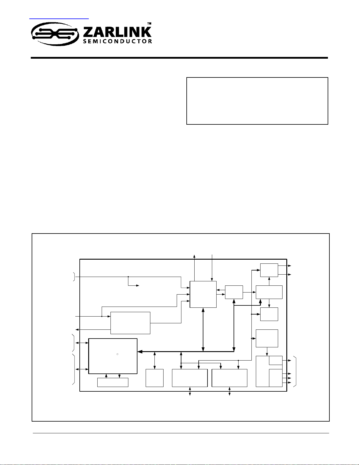
ZL10310 / ZL10311 DTV-SOC
EXTIN
JTAG
ADCIN
AUX Bus
PowerPC 405
Sub System
2
Peripherals
Power Management
Cached
COFDM
DeModulator
& FEC
R
8k Boot
ROM
Multiplexing &
SDRAM
Controller
SDRAM 1
BUS
Bitstream
Control
De-
scrambler
SDRAM
Controller
SDRAM 0
BUS
(optional)
Audio
Decoder
System
DeMultiplex
Video
Decoder
Video Scaler
/ Blender
Comp
Video
Video
DENCs
/DACs
Y+U/V
RGB
I S
DAC
S/PDIF
Analog
Video
Figure 1 - Block Diagram of ZL10310 and ZL10311
1

ZL10310/ZL10311 Data Sheet
Applications
• Low power, small footprint TV adaptors
• Integrated Digital Televisions (iDTV)
• Digital terrestrial set-top boxes
• DTT / DVD Combo
• DVB-T radio receivers
• Terrestrial / Satellite Combo
• Terrestrial / Cable Combo
• Terrestrial / IP (Internet Protocol) Combo
Description
Zarlink Semiconductor has responded to market demand by integrating its key DVB-T compliant COFDM
demodulation technology with Set Top Box functionality (MPEG-2 A/V decoder and system interfaces) together with
a high performance CPU to offer a “DVB-T On-a-Chip” solution.
The ZL10310 DVB-T On-a-Chip, can address a wide range of DVB-T consumer electronic products. At the entry
level it can be used to build ultra-compact Free-To-View Digital TV adaptors (such as for FreeView in the UK), yet
consumes less than 4W of power in full operational mode.
This level of compactness also considerably eases the integration of DVB-T receiver technology inside integrated
Digital TV sets (iDTV’s) where space considerations and thermal management are key design issues.
TM
The ZL10310 is based upon an industry standard PowerPC 405
Management sub-systems. This permits the device to be effectively deployed in compelling applications such as
interactive Digital TV which are able to exploit the superior processing performance offered by the PowerPC
processor core.
The PowerPC
provides an ideal platform for running robust open standard operating systems such as Linux which
can benefit system developers in a number of key areas:
RISC processor, which has Virtual and Memory
• Unified software development environment, from entry level basic channel zapper systems through to fully
interactive high performance Digital Set Top Boxes.
• Re-use of software code from multiple projects
• Exploit software code developed in the Linux community.
• Low cost-per-seat software development environment.
• Familiar software development environment.
• Royalty free.
Also available is the ZL10311 DVB-T On-a-Chip, which additionally offers Dolby
decoding, and Macrovision
TM
Copy Protection for applications requiring Dolby Audio and Pay TV services.
Digital1 multi-channel audio
1. The ZL10311 device is awaiting Dolby Certification
2 Zarlink Semiconductor Inc.

Data Sheet ZL10310/ZL10311
Table of Contents
1.0 Device Overview . . . . . . . . . . . . . . . . . . . . . . . . . . . . . . . . . . . . . . . . . . . . . . . . . . . . . . . . . . . . . . . . . . . . . . . 4
2.0 Device Interfaces . . . . . . . . . . . . . . . . . . . . . . . . . . . . . . . . . . . . . . . . . . . . . . . . . . . . . . . . . . . . . . . . . . . . . . . 4
3.0 Typical Digital Television (DTV) Receiver . . . . . . . . . . . . . . . . . . . . . . . . . . . . . . . . . . . . . . . . . . . . . . . . . . . 5
4.0 Functional Blocks Overview . . . . . . . . . . . . . . . . . . . . . . . . . . . . . . . . . . . . . . . . . . . . . . . . . . . . . . . . . . . . . . 6
4.1 Boot ROM . . . . . . . . . . . . . . . . . . . . . . . . . . . . . . . . . . . . . . . . . . . . . . . . . . . . . . . . . . . . . . . . . . . . . . . . . . 6
4.2 Clock Generation Block . . . . . . . . . . . . . . . . . . . . . . . . . . . . . . . . . . . . . . . . . . . . . . . . . . . . . . . . . . . . . . . . 6
4.3 Coded Orthogonal Frequency Division Multiplex (COFDM) Demodulator . . . . . . . . . . . . . . . . . . . . . . . . . 7
4.4 MPEG Audio Decoder . . . . . . . . . . . . . . . . . . . . . . . . . . . . . . . . . . . . . . . . . . . . . . . . . . . . . . . . . . . . . . . . . 7
4.5 MPEG-2 Video Decoder . . . . . . . . . . . . . . . . . . . . . . . . . . . . . . . . . . . . . . . . . . . . . . . . . . . . . . . . . . . . . . . 8
4.6 PowerPC 405TM Processor . . . . . . . . . . . . . . . . . . . . . . . . . . . . . . . . . . . . . . . . . . . . . . . . . . . . . . . . . . . . 8
4.7 Transport Engine . . . . . . . . . . . . . . . . . . . . . . . . . . . . . . . . . . . . . . . . . . . . . . . . . . . . . . . . . . . . . . . . . . . . . 9
4.8 Video Display System . . . . . . . . . . . . . . . . . . . . . . . . . . . . . . . . . . . . . . . . . . . . . . . . . . . . . . . . . . . . . . . . . 9
5.0 Physical Specification . . . . . . . . . . . . . . . . . . . . . . . . . . . . . . . . . . . . . . . . . . . . . . . . . . . . . . . . . . . . . . . . . . 10
6.0 ZL10310/ZL10311 388-pin Package Pin Descriptions. . . . . . . . . . . . . . . . . . . . . . . . . . . . . . . . . . . . . . . . . 11
6.1 Pin Types. . . . . . . . . . . . . . . . . . . . . . . . . . . . . . . . . . . . . . . . . . . . . . . . . . . . . . . . . . . . . . . . . . . . . . . . . . 11
6.2 Front End Interfaces . . . . . . . . . . . . . . . . . . . . . . . . . . . . . . . . . . . . . . . . . . . . . . . . . . . . . . . . . . . . . . . . . 11
6.3 Video DAC Outputs . . . . . . . . . . . . . . . . . . . . . . . . . . . . . . . . . . . . . . . . . . . . . . . . . . . . . . . . . . . . . . . . . . 14
6.4 SDRAM Interfaces . . . . . . . . . . . . . . . . . . . . . . . . . . . . . . . . . . . . . . . . . . . . . . . . . . . . . . . . . . . . . . . . . . . 15
6.5 Bit Stream Interfaces . . . . . . . . . . . . . . . . . . . . . . . . . . . . . . . . . . . . . . . . . . . . . . . . . . . . . . . . . . . . . . . . . 17
6.6 Auxiliary External Bus . . . . . . . . . . . . . . . . . . . . . . . . . . . . . . . . . . . . . . . . . . . . . . . . . . . . . . . . . . . . . . . . 21
6.7 Peripheral Port. . . . . . . . . . . . . . . . . . . . . . . . . . . . . . . . . . . . . . . . . . . . . . . . . . . . . . . . . . . . . . . . . . . . . . 24
6.8 Modem/Codec Interface . . . . . . . . . . . . . . . . . . . . . . . . . . . . . . . . . . . . . . . . . . . . . . . . . . . . . . . . . . . . . . 26
6.9 Smart Card Interface . . . . . . . . . . . . . . . . . . . . . . . . . . . . . . . . . . . . . . . . . . . . . . . . . . . . . . . . . . . . . . . . . 28
6.10 General Purpose Input Output Interfaces . . . . . . . . . . . . . . . . . . . . . . . . . . . . . . . . . . . . . . . . . . . . . . . . 28
6.11 Simplified General Purpose Input Output Interface . . . . . . . . . . . . . . . . . . . . . . . . . . . . . . . . . . . . . . . . . 31
6.12 Inter Integrated Circuit (I2C) Interface . . . . . . . . . . . . . . . . . . . . . . . . . . . . . . . . . . . . . . . . . . . . . . . . . . . 33
6.13 Inter IC Sound (I2S) Audio Interface . . . . . . . . . . . . . . . . . . . . . . . . . . . . . . . . . . . . . . . . . . . . . . . . . . . . 33
6.14 Clock and Reset Interface . . . . . . . . . . . . . . . . . . . . . . . . . . . . . . . . . . . . . . . . . . . . . . . . . . . . . . . . . . . . 33
6.15 Power Supply Pins . . . . . . . . . . . . . . . . . . . . . . . . . . . . . . . . . . . . . . . . . . . . . . . . . . . . . . . . . . . . . . . . . 34
6.16 Reserved Connections . . . . . . . . . . . . . . . . . . . . . . . . . . . . . . . . . . . . . . . . . . . . . . . . . . . . . . . . . . . . . . 35
7.0 Characteristics . . . . . . . . . . . . . . . . . . . . . . . . . . . . . . . . . . . . . . . . . . . . . . . . . . . . . . . . . . . . . . . . . . . . . . . . 36
7.1 AC and DC Electrical Characteristics . . . . . . . . . . . . . . . . . . . . . . . . . . . . . . . . . . . . . . . . . . . . . . . . . . . . 36
®
IBM
, the IBM Logo, PowerPC® and PowerPC405TM are trademarks of International Business Machines
Corporation.
Dolby
is a trademark of Dolby Laboratories. Supply of this implementation of Dolby Technology does not convey a
license or imply a right under any patent, or any other Industrial or Intellectual Property Right of Dolby Laboratories,
to use this implementation in any finished end-user or ready-to-use final product. It is hereby notified that a license
for such use is required from Dolby Laboratories
1
.
This device is protected by US patent numbers 4631603, 4577216 and 4819098 and other intellectual property
rights. Use of the Macrovision anticopy process in the device is licensed by Macrovision for non-commercial, home
and limited exhibition use only. Reverse engineering or disassembly is prohibited. A valid Macrovision license must
be in effect between the purchaser of the ZL10311 IC and Macrovision Corporation. Additional per-chip royalties
may be required and are payable by the purchaser to Macrovision.
1. The ZL10311 device is awaiting Dolby Certification
3Zarlink Semiconductor Inc.

ZL10310/ZL10311 Data Sheet
1.0 Device Overview
Zarlink Semiconductor has designed the ZL10310 and ZL10311 System On a Chip (SoC) devices specifically for
DVB-T applications. Integrating a high performance PowerPC 405
MPEG-2 audio and video decoding, OSD and a COFDM demodulator, the ZL10310 and ZL10311 deliver the
performance and functionality required for advanced Digital TV entertainment products. It enables the rapid design
and manufacture of cost-effective iDTV and Digital Audio Visual Home Entertainment Centers.
The enhanced ZL10311 also supports DVD playback with up to six Dolby
integrating the COFDM demodulator, the ZL10310 and ZL10311 enable the implementation of very small footprint
TV Adaptor modules.
2.0 Device Interfaces
The following peripheral interfaces are available to the user. Apart from possible level translation and connector
buffering, no external devices are required to support any of the interfaces.
• 10-bit input that may be configured for an ADC input to the internal COFDM demodulator
• Additional input bus for additional MPEG-2 Transport Sources
• AGC (PWM) outputs for a terrestrial tuner
• Serial control port for a digital tuners
• Common interface control and bitstream interfaces for an external descrambler
• Normal PC (PCMCIA) memory module interface for local software updates
• Unified 64 Mbit SDRAM interface for all decoders and PowerPC 405
• Additional SDRAM interface for high end systems requiring increased memory bandwidth
• Static memory interface for Flash and external peripherals
• IDE/ATAPI interface for hard disk and DVD drives
• External DMA channel and interrupts
• Six analog video outputs give full flexibility on RGB, S-VHS, and composite signals (with and without OSD)
2
S input port from external Digital Stereo source
•I
•Three I
•Dolby
• Sony/Philips Digital InterFace (S/PDIF)
2
S ports to external audio DACs for main, surround, and centre channels
surround sound control signals
TM
processor with robust industry proven
Digital1 audio channels. In addition, by
TM
If not required in a particular system, any of the peripheral interfaces can be replaced by individual I/O bits from
internal general purpose registers. These can then be used for additional purpose, such as interfacing to switches
and displays.
• Full RS232 interface to an external modem or a 4 wire interface to a Codec
• IRDA interface or an additional asynchronous serial interface
• Synchronous serial interface for EEPROM, etc.
• Two Smart card Interfaces (one instead of a Common Interface)
2
• General purpose I
C interface
• General purpose timer for Infrared (IR) decoding
• General purpose individual bit I/Os
1. The ZL10311 device is awaiting Dolby Certification
4 Zarlink Semiconductor Inc.
Data Sheet ZL10310/ZL10311
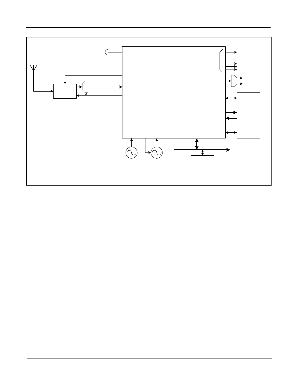
InfraRed Sens or
Analog Video
Terrestrial
Tuner
Tuner Control
A
D
C
20.48MHz
ADCIN
AGC B
ADCCLK
COFDM
Clock
20.48MHz
Crystal
Oscillator
ZL10310
DTV-SOC
CLK
27IN
Error
Aux Bus
27MHz
VCXO
Aux
Bus
FLASH
Digital Audio
8MB
(I S)
Common
Interface
SDRAM1
Bus
2
Figure 2 - Block diagram of a typical ZL10310-based Free to Air TV Adaptor
Comp Video
RGB or Y U/V
D
A
Analog Audio
C
Serial
EEPROM
Bitstream o/ps
Bitstream i/ps
SDRAM
External
Peripherals
3.0 Typical Digital Television (DTV) Receiver
Figure 2 shows a typical Free to Air TV receiver block diagram employing a ZL10310 DTV-SoC device. In its
minimal configuration, the ZL10310 DTV-SoC device only requires a single 64 Mbit SDRAM, an audio DAC, and a
Flash ROM, which are in addition to a DVB-T tuner front end and a 10-bit analog to digital converter.
The Terrestrial Tuner section performs an independent down conversion of the received DVB-T signal from the
Antenna, to an IF frequency in the range of 30MHz to 57MHz, dependent on television system (typically 36.17MHz
Center Frequency, with ±4MHz span). The analogue IF is then converted to the digital domain, with a 10-bit ADC,
clocked at 20.48MHz and the resulting Digital output is centered on 15.69MHz. This Digital signal is applied to the
ZL10310 via the ADC_IN[9:0] input pins, in the form of a 10-bit parallel signal.
The ZL10310 converts the digitized IF from a Terrestrial TV Tuner into an MPEG-2 Transport Stream, which can be
optionally de-scrambled (if CA scrambling is used by the broadcaster), and de-multiplexed into separate Packetised
Elementary Streams (PES), which are routed to the MPEG Audio and Video decoders, and SI data to the PowerPC
TM
subsystem.
405
Decoded Video can then be mixed and optionally scaled with On-Screen Display (OSD) Graphics generated by the
DTV application software. The resultant combination of video and graphics are then routed to the PAL/NTSC Digital
ENCoders (DENCs) for display on the TV via the on-chip 10-bit video DACs.
2
Decoded Audio is output directly from the audio decoder sub-system to the I
InterFace) outputs.
S and S/PDIF (Sony/Philips Digital
5Zarlink Semiconductor Inc.

ZL10310/ZL10311 Data Sheet
4.0 Functional Blocks Overview
4.1 Boot ROM
Program execution on the Power PC normally starts from address 0xFFFFFFFC after the internal reset has gone
inactive. This would normally be an address in the external Flash ROM (enabled by BI_CS0), but, by forcing the
SGPIO2_3 pin low during reset, it is possible to boot from the Internal 8k Boot ROM. The ZL10310 and ZL10311
devices contain an 8k Boot ROM containing code, which is executed under the noted conditions above following a
complete system reset (i.e. when main power has been removed from the ZL10310 or ZL10311).
The code installed on the Boot ROM, allows the ZL10310/ZL10311 to undertake any of the following 4 functions
after a complete reset:
1. Enter ISP (in-system programmable) mode, in which the software in the internal Boot ROM will try booting from
2
an SPI or I
2. Try booting from an Atmel Serial Flash device (AT45xxxxx) first, if that fails then enter ISP mode.
3. Try booting from an asynchronous parallel flash device connected to the EBIU bus (CS0) first. If that fails, then
try booting from SPI or I
4. Enter debug/monitor mode in which a command prompt is available for debugging registers, downloading code,
etc.
4.2 Clock Generation Block
C EEPROM.
2
C EEPROM or Serial Flash.
The ZL10310/ZL10311 devices use two separate external clock sources to provide all the clocks required; a 27MHz
external Voltage Controlled crystal Oscillator (VCXO), and a 20.48MHz external Crystal Oscillator.
A standard 27MHz input to the systems PLL is supplied from an external VCXO. Outputs from this PLL are used to
clock the various internal MPEG decoders, the PowerPC
micro controller system, and the external SDRAM. The
frequency can be adjusted in the ppm range, using a voltage produced by the pulse width modulated frequency
error signal, available from GPIO port GP29.
The 27MHz input also drives a separate audio PLL that is dedicated to providing 256/512 times the audio sampling
rate for the audio decoder and external audio DAC.
The COFDM de-modulators have their own PLL driven from an internal 20.48MHz oscillator. An external crystal is
required for this oscillator.
6 Zarlink Semiconductor Inc.

Data Sheet ZL10310/ZL10311
4.3 Coded Orthogonal Frequency Division Multiplex (COFDM) Demodulator
The COFDM demodulator is used to demodulate a digitized COFDM modulated IF signal from the TV Tuner, and
ultimately convert the resulting MPEG-2 Transport Stream to the MPEG-2 demultiplexer.
The Digitized IF is converted to a complex Baseband signal centered on zero frequency. It also removes adjacent
channel interference prior to a Time-to-Frequency Fast Fourier Transform (FFT). The resulting signals are then sent
to a digital re-timing block, symbol sync, carrier recovery, and timing recovery. An AGC signal, with a variable mark
space ratio, is provided to control the signal levels in the tuner sections of the receiver. Forward Error Correction
(FEC) is performed by Viterbi decoding of the convolutional coded data, followed by de-interleaving, Reed-Solomon
decoding, and energy dispersal de-randomising. The output is MPEG-2 Transport Stream packets, in byte format.
The COFDM demodulator is fully compliant with the ETSI 300 744 and Digital Television Group (DTG)
specifications. Key features are:
1
• FFT processor operates in 2k and 8k carrier mode.
• All hierarchical and non-hierarchical constellations.
• Automatic digital carrier recovery over a wide range of offsets without the need for AFC
• Automatic digital carrier recovery without the need for a VCXO
• Common phase error correction
• Channel correction using time and frequency filtering
• Automatic co - channel protection, frame sync, and fast channel re- acquisition
• Internal controller handles all tracking and acquisition
• Viterbi decoding with code rates of 1/2, 2/3, 3/4, 5/6, 6/7, and 7/8
• Automatic synchronization and code rate detection
• Constraint length K = 7
• Trace back depth of 128
• De-interleaver followed by DVB Reed Solomon error correction
• De-randomizer and common interface formatting
4.4 MPEG Audio Decoder
The MPEG Audio Decoder produces dual channel outputs from MPEG -1 or MPEG -2 Transport Streams with a
maximum rate of 640 kbit/sec. It supports sampling rates of 32, 44.1, and 48 KHz, plus the half rate options. All
sampling rates, plus 512/256 Fs, are produced from an internal PLL. A version of the device is available which
produces six channels of audio output for holders of the Dolby
• Decodes MPEG-1 and dual channel MPEG-2 audio
• Performs MPEG-1 audio parsing and MPEG-2 Packetised Elementary Stream (PES) audio parsing, or
accepts audio elementary streams
• Supports 32kHz, 44.1 kHz, and 48 kHz sampling rates plus the half rate options
• All sampling rates, plus 512/256 Fs, derived from an internal PLL
• 64 step audio attenuation with smooth step transitions
• SPDIF output meeting IEC1937 specifications
• Re-locatable ancillary data region
• Audio Clip Mode
• Dolby
1. For details on 8k carrier performance and use, please consult Zarlink Field Applications
2. The ZL10311 device is awaiting Dolby Certification
AC3 option
2
Digital2 License.
7Zarlink Semiconductor Inc.

ZL10310/ZL10311 Data Sheet
4.5 MPEG-2 Video Decoder
The MPEG-2 Video Decoder provides complete decoding and synchronized playback of MPEG-2 MP@ML (Main
Profile at Main Level) video streams. It supports the decoding of still pictures as well as moving video, with error
concealment when necessary. A command driven local controller minimizes the amount of application software
needed to control the decoding / channel change process.
The decoder accepts PES from the Transport De-multiplexer, with average rates of up to 15 Mbps. PES header
parsing supports the extraction of Presentation Time Stamp (PTS) values, which are then used by the audio/ video
synchronization hardware. PES or ES streams can be directly decoded from SDRAM in the Video Clip mode of
operation.
Feature summary:
• Packetised MPEG-2 MP @ ML video streams from the transport demultiplexer or from SDRAM
• MPEG-1 video (ES) streams from SDRAM
• Sustained bit rates from 1.5 Mbps to 15 Mbps.
• Local processor driven by commands from the application processor
• Sophisticated error concealment based on the use of stored motion vectors from the previous row
• Supports the decoding of still images
• Automatic or manual image re-sizing
• Conversion of MPEG-1, 24 Hz progressive scan, pictures to 60 Hz interlaced (3:2 pull-down)
4.6 PowerPC 405TM Processor
An integrated PowerPC 405TM processor core is provided for applications and control software, and this provides
approx. 150 Drhystone MIPS with a clock of 108 MHz.
It has instruction and data caches with lock down facilities such that defined areas can be used as general purpose
ram. The processor has its own internal bus to which is attached the caches, all the peripherals, and a DMA
controller. Code can thus be executed, using internal resources, whilst the MPEG decoders are using the SDRAM.
This processor bus is also connected to an auxiliary external bus, which is used for Flash code transfer during the
power on routine, and for Flash write operations. PCMCIA, and IDE data transfers also use this bus to provide data
and address signals, but their respective control signals have dedicated pins. A bridge to the internal multi-master
bus provides software access to the external SDRAM.
All internal and external memory is in a unified address space, and a DMA controller supports high speed data
transfers. Controllers are provided for two smart cards, an RS232 modem, a serial Codec, an I
synchronous serial port, and an IRDA interface. Individual bit I/O is also supported.
Key Features:
TM
• PowerPC 405
Processor Core running at 108 MHz
• Integrated instruction and data caches (16k/16k) with lock down
• Integrated set top box peripheral controllers
• Four channel DMA controller for peripheral and data transfers
• Dedicated internal processor bus with its own SDRAM controller and auxiliary bus
• Bridge to the decoder multi-master bus and shared SDRAM
•Real Time Counters
• Watch dog timer
• Interrupt Controller
2
C master, a
8 Zarlink Semiconductor Inc.

Data Sheet ZL10310/ZL10311
4.7 Transport Engine
The ZL10310/ZL10311 devices contain a dedicated hardware implementation of an MPEG/DVB transport stream
de-multiplexer, with the configuration of this hardware controlled by application software. Included in the hardware
are synchronization, Packet Identifier (PID) filtering, clock recovery, de-scrambling, and table section filtering. PID
filtered packets are stored in a local buffer, which can hold up to 10 packets before they are moved to the decoders
or to memory queues in SDRAM. The queues are used for the tables containing system information. Packets for
three destinations can be moved concurrently out of the buffer.
The hardware acts in conjunction with a Transport Assist Processor, and the resultant hardware/software
combination gives increased adaptability and extended processing capability. Further parsing and filtering is
possible, and interrupts can be generated to notify the processor when a given condition has been met. The
transport assist processor can then read and manipulate packets whilst they are still in the transport packet buffer.
It can then allow data to pass through to SDRAM or the decoders, or can record status information and optionally
interrupt the application.
Key Features:
• 32 PID values can be used to filter the transport stream
• Flexible, hardware based, section filtering
• 64, 4 byte, filter blocks.
• Filter blocks can be cascaded to provide deep filtering when necessary
• Hardware Cyclical Redundancy Check (CRC) checking
• Captured data is transferred to one of thirty two queues in SDRAM
• Options to transfer complete transport packets with or without headers, or sections
• Adaptation fields can be delivered to a separate queue
• Hardware to extract PCR values with option for software filtering to remove long term jitter
• Comprehensive error detection hardware
• Integrated DVB descrambler
4.8 Video Display System
The Video Display System provides multi-layered video. This features the On-Screen Display (OSD) for menuing
and MHEG-5, the Decoded Video Presentation system, and a Video Blending capability to merge the OSD and
Video.
The On-Screen Display system is designed to meet or exceed the specifications of major European broadcasters.
The final image on the screen is constructed from five separate planes using a fixed display hierarchy. The screen
hierarchy consists of:
1. Cursor plane (Top)
2. Region-based graphics plane (typically used for EPG and System menus)
3. Video plane
4. Still image plane (typically used for MHEG-5)
5. Background plane
All planes, apart from the background plane, can be separately enabled. The graphics and image planes are region
based, and driven by means of bitmaps controlled by a link-list processor. They can operate independently, but
have nearly identical operational controls. The size of a bitmap region can vary between 4 pixels wide by 2 pixels
deep, and 1K pixels wide and 1K pixels deep. The color resolution of a pixel within a region can be defined by 2, 4,
8, or 16 bits. The 16-bit option is for direct colors; the other options use color look up tables.
The Video Presentation system is used to scale and process a decoded Video signal. Decoded Video is stored in
Field Stores contained in external SDRAM memory. Prior to display it can be automatically scaled from the original
resolution and aspect ratio up to PAL or NTSC full screen size. If the encoded image has a 16:9 aspect ratio, but
the display has a 4:3 aspect ratio, then any horizontal scaling factor necessary to fill the screen must be adjusted by
9Zarlink Semiconductor Inc.
ZL10310/ZL10311 Data Sheet
Pin A1
a further factor of 4/3. Alternatively, a factor of 3/4 can be applied vertically (letter box mode). Video is displayed at
the standard PAL or NTSC field rates. Synchronization signals for video presentation can be provided by either the
video decoder itself (master mode), or the decoder can slave to incoming signals.
The Video Blending System is used to blend the outputs from separate Digital Encoded Video (DENC) blocks for
the Video and OSD systems on-chip:
1. RGB – Red Green Blue
2. Y U/V
3. CVBS – Chroma Video Blanking and Sync
5.0 Physical Specification
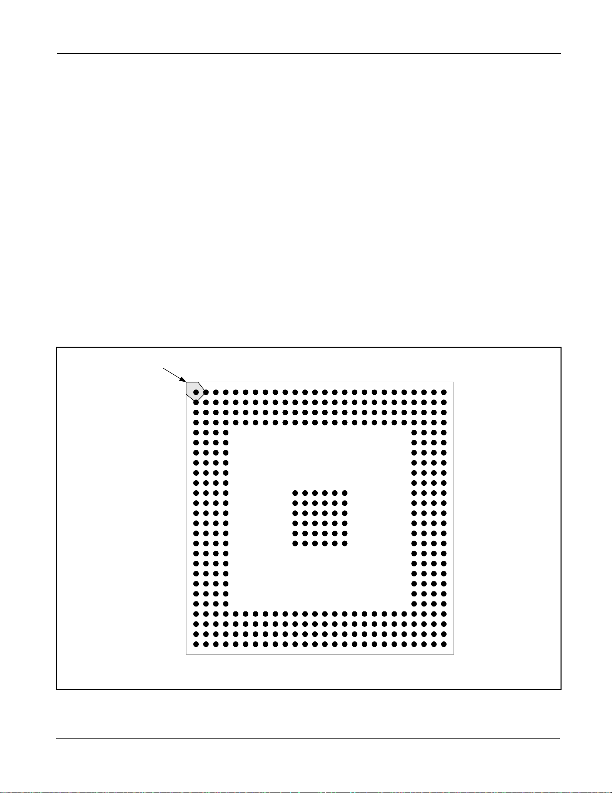
The device is contained in a 388-ball Enhanced Plastic Ball-Grid Array (388 EPBGA) package:
• Body Size: 27mm x 27mm
• Ball Count: 388 (includes 36 Thermal Balls)
• Ball Pitch: 1.0mm
• Ball Matrix: 26 x 26 (partially populated with a 6 x 6 GND matrix in the centre)
• Ball Diameter 0.60mm
• Total Package Thickness 2.65mm
Package is viewed from the top side (i.e. through top of the package). Note ball A1 is non-chamfered corner.
Pin A1
ident
ident
B
D
F
H
K
M
P
T
V
Y
AB
AD
AF
123456789
A
C
E
G
J
L
N
R
U
W
AA
AC
AE
10
11
12
13
14
15
16
17
18
19
20
21
22
23
24
26
25
A
B
C
D
E
F
G
H
J
K
L
M
N
P
R
T
U
V
W
Y
AA
AB
AC
AD
AE
AF
123456789
11
10
12
13
14
15
16
Figure 3 - Package View and Ball Positions
10 Zarlink Semiconductor Inc.
17
18
19
20
21
22
23
24
25
26

Data Sheet ZL10310/ZL10311
6.0 ZL10310/ZL10311 388-pin Package Pin Descriptions
This section explains the ZL10310 and ZL10311 device pin functions. The following tables are segmented by signal
functions. Many of the pins listed below have multiple functions, and in these cases there is information on how the
multiplexed function connects to the pin.
Many references are made to register settings throughout the Pin Descriptions. The details of the ZL10310 and
ZL10311 registers can be found in the Hardware Design Manual for the ZL103xx family of Integrated Digital
Television Processors (Publication DM5797), available to customers on request, subject to NDA.
6.1 Pin Types
I An Input Type with no designator indicates that the signal must be produced by a device using 3.3V
outputs, and ESD protection is provided. There is no internal pull up, so unused inputs should be
tied high or low.
IO Pin Type indicates that the pin can be programmed with control bits to be used as an input or an
output.
B Pin Type indicates that the pin function can alternate between an input and output depending on the
use at that instant i.e. it is Bi-directional. Out characteristics are the same as an Out pin.
OD is an open drain Output.
O
5V is a 5V tolerant Input or Output. An Input Type with a 5V designator indicates that the input tolerates
is a standard 3.3 V, 65 ohm, output, unless otherwise specified. DC drive is 8.2mA/5.4mA @ VH/VL
respectively. Maximum slew rate is 75mA/ns, unless otherwise specified.
5V signals. There is no internal pull up.
6.2 Front End Interfaces
Pin Name
ADCCLK R02 ADCCLK O Sampling Clock Output to External Tuner IF
AGC[0] L02 Tuner AGC control O 5V Master AGC Control Output to External TV Tuner 1
AGC[1] M03 Tuner AGC control
GPP[0] L01 Tuner_SCL O 5V External TV Tuner Control Bus - Clock Output 1, 6
GPP[1] N04 Tuner_SDA B 5V External TV Tuner Control Bus - Data
EXT_IN[0] K01 ED1_MDO[7]
Pin
No.
Function
offset
(MSB)
Pin
Type
Analog to Digital Converter. Clock = 20.48MHz.
O 5V Secondary AGC Control Output to External TV
Tuner. Used to provide a differential AGC feed to
external TV Tuner, if required.
Input/Output.
I External Demodulator 1 Digital Input -
Data Bit 7 (MSB)
Description Notes
1
1, 6
5, 7
DV2_IN_DATA[7]
(MSB)
RW_TDO O Debug Interface - JTAG TDO (Data Out) 3
I Reserved 7
11Zarlink Semiconductor Inc.

ZL10310/ZL10311 Data Sheet
Pin Name
EXT_IN[1] K02 ED1_MDO[6] I 5V External Demodulator 1 Digital Input - Data Bit 6 1, 5, 7
EXT_IN[2] J01 ED1_MDO[5] I External Demodulator 1 Digital Input - Data Bit 5 5, 7
EXT_IN[3] L03 ED1_MDO[4] I External Demodulator 1 Digital Input - Data Bit 4 5, 7
EXT_IN[4] J02 ED1_MDO[3] I External Demodulator 1 Digital Input - Data Bit 3 5, 7
Pin
No.
Function
RW_TDI I 5V Debug Interface - JTAG TDI (Data In) 1, 3
DA_SER_DATAI I 5V Digital Audio Serial Data Input. Main left and right
DV2_IN_DATA[6] I Reserved 7
RW_HALT I Debug Interface - JTAG Halt 3
DV2_IN_DATA[5] I Reserved 7
RW_TMS I Debug Interface - JTAG TMS 3
DV2_IN_DATA[4] I Reserved 7
RW_TCK I Debug Interface - JTAG TCK 3
Pin
Typ e
Description Notes
1, 4
serial audio data at a rate of 64fs. Signal routed
through to GP12 (not bonded out)
EXT_IN[5] L04 ED1_MDO[2] I External Demodulator 1 Digital Input - Data Bit 2 5, 7
DV2_IN_DATA[3] I Reserved 7
Tes t[ 0] I Tes t M od e A - Tes t P in 0
EXT_IN[6] K03 ED1_MDO[1] I External Demodulator 1 Digital Input - Data Bit 1 5, 7
DV2_IN_DATA[2] I Reserved 7
Tes t[ 1] I Tes t M od e A - Tes t P in 1
EXT_IN[7] H02 ED1_MDO[0]
(LSB)
DV2_IN_DATA[1] I Reserved 7
Tes t[ 2] I Tes t M od e A - Tes t P in 2
EXT_IN[8] G01 ED1_MVAL I External Demodulator 1 Digital Input - Data Valid
DV2_IN_DATA[0]
(LSB)
Tes t[ 3] I Tes t M od e A - Tes t P in 3
EXT_IN[9] J03 ED1_MCLK I External Demodulator 1 Digital Input - Clock Input 5
I External Demodulator 1 Digital Input - Data Bit 0
(LSB)
Input
I Reserved 7
5, 7
5
DV2_Pixel_Clk I Reserved
Tes t[ 4] I Tes t M od e A - Tes t P in 4
12 Zarlink Semiconductor Inc.

Data Sheet ZL10310/ZL10311
Pin Name
ADC_IN[0] V03 COFDM_ADCIN[8]
ADC_IN[1] W03 COFDM_ADCIN[7] I COFDM Digital Input from Ext. ADC - Data Bit 7 2, 5, 7
ADC_IN[2] AA02 COFDM_ADCIN[6] I COFDM Digital Input from Ext. ADC - Data Bit 6 2, 5, 7
ADC_IN[3] AB01 COFDM_ADCIN[5] I COFDM Digital Input from Ext. ADC - Data Bit 5 2, 5, 7
Pin
No.
Function
(MSB)
DV2_IN_DATA[7]
(MSB)
ED2_MDO[7]
(MSB)
ED2_MDO[6] I External Demodulator 2 Digital Input - Data Bit 6
DV2_IN_DATA[6] I Reserved (when EXT_IN[2] used for JTAG in
ED2_MDO[5] I External Demodulator 2 Digital Input - Data Bit 5 7
DV2_IN_DATA[5] I Reserved (when EXT_IN[3] used for JTAG in
Pin
Type
I COFDM Digital Input from Ext. ADC - Data Bit 8
(MSB)
I Reserved (when EXT_IN[0] used for JTAG in
Debug)
I External Demodulator 2 Digital Input - Data Bit 7
(MSB)
Debug)
Debug)
Description Notes
2, 5, 7
7
7
7
7
ED2_MDO[4] I External Demodulator 2 Digital Input - Data Bit 4 7
ADC_IN[4] Y03 COFDM_ADCIN[4] I COFDM Digital Input from Ext. ADC - Data Bit 4 2, 5, 7
DV2_IN_DATA[4] I Reserved (when EXT_IN[4] used for JTAG in
Debug)
ED2_MDO[3] I External Demodulator 2 Digital Input - Data Bit 3 7
ADC_IN[5] AB02 COFDM_ADCIN[3] I COFDM Digital Input from Ext. ADC - Data Bit 3 2, 5, 7
DV2_IN_DATA[3] I Reserved (when EXT_IN[5] used for JTAG in
Debug)
ED2_MDO[2] I External Demodulator 2 Digital Input - Data Bit 2 7
ADC_IN[6] AC01 COFDM_ADCIN[2] I COFDM Digital Input from Ext. ADC - Data Bit 2 2, 5, 7
DV2_IN_DATA[2] I Reserved 7
ED2_MDO[1] I External Demodulator 2 Digital Input - Data Bit 1 7
ADC_IN[7] AA04 COFDM_ADCIN[1] I COFDM Digital Input from Ext. ADC - Data Bit 1 2, 5, 7
DV2_IN_DATA[1] I Reserved 7
ED2_MDO[0]
(LSB)
I External Demodulator 2 Digital Input - Data Bit 0
(LSB)
7
7
7
13Zarlink Semiconductor Inc.

ZL10310/ZL10311 Data Sheet
Pin Name
Pin
No.
Function
ADC_IN[8] AA03 COFDM_ADCIN[0]
(LSB)
DV2_IN_DATA[0]
Pin
Typ e
Description Notes
I COFDM Digital Input from Ext. ADC -
Data Bit 0 (LSB)
I Reserved 7
2, 5, 7
(LSB)
ED2_MOVAL I External Demodulator 1 Digital Input -
Data Valid Input
ADC_IN[9] AC02 DV2_IN_Pixel_Clk I Reserved
ED2_MOCLK I External Demodulator 1 Digital Input - Clock Input
Note 1: 5V tolerant connection to allow use of 5V Tuner devices
Note 2: Multiplex setup with COFDM Register Bit 0 = '1'
Note 3: Multiplex setup with CICSEL3 Register Bits 9:11 = '111'
Note 4: Multiplex setup with CICSEL3 Register Bit 6 = '1', and GPIS2 Register Bits 24:25 = '01'
Note 5: Multiplex setup with COFDM Register Bit 0 = '0'
Note 6: External pull-up to Tuner Vdd PSU required on GPPx lines.
Note 7: The ADC_IN [0:9] and EXT_IN [0:9] inputs on the Front End interface are configured as “Big Endian”. This means that bit [0]
Note 8: When the ADC_IN [0:9] and EXT_IN [0:9] pins are used to provide various alternative inputs within one application, then each
is the Most Significant Bit (MSB) for the multiplexed functions mapped to that pin.
set of inputs must have a tri-state buffer. The enables for these buffers should then be controlled by general purpose I/O pins.
6.3 Video DAC Outputs
Pin Name Pin No.
Pin
Typ e
Description Notes
DAC_OP0 AE15 O Video Triple-DAC 1 output 1. 1, 2
DAC_OP1 AD15 O Video Triple-DAC 1 output 2. 1, 2
DAC_OP2 AD13 O Video Triple-DAC 1 output 3. 1, 2
DAC_OP3 AD10 O Video Triple-DAC 2 output 1. 1, 2
DAC_OP4 AF06 O Video Triple-DAC 2 output 2. 1, 2
DAC_OP5 AF10 O Video Triple-DAC 2 output 3. 1, 2
DAC1_CREF_OUT AF11 O De-coupling for triple DAC 1 - to GND
DAC1_GREF_OUT AF17 O De-coupling for triple DAC 1 - to AVDD
DAC1_RREF_OUT AE13 O Gain control for triple DAC 1. 3
DAC1_VREF_IN AE14 I Voltage reference input (1.2V) for Video Triple-DAC 1. 4
DAC2_CREF_OUT AE11 O De-coupling for triple DAC 2 - to GND
DAC2_GREF_OUT AF05 O De-coupling for triple DAC 2 - to AVDD
DAC2_RREF_OUT AE09 O Gain control for triple DAC 2. 3
DAC2_VREF_IN AF07 I Voltage reference input (1.2V) for Video Triple-DAC 2 4
Note 1: Video outputs capable of driving between 37.5ohm and 75ohm loads.
14 Zarlink Semiconductor Inc.

Data Sheet ZL10310/ZL10311
Note 2: Triple DAC output can be setup using the DENCMUX register to output any of the following types of video signal:
Note 3: Gain set using Current Adjust resistor to GND. Typically need 392ohms for a DAC load of 37.5ohms.
Note 4: Apply external reference (1.2V) when internal reference is not in use.
6.4 SDRAM Interfaces
RGB, CVBS, Y U/V
The ZL10310 and ZL10311 devices have 2 independent SDRAM interfaces. The main SDRAM interface is
SDRAM1 which is used as the main memory space for both the PowerPC
processor and Video/Audio decoding. If
required a separate processor-only SDRAM interface can be used; this is the optional SDRAM0 interface.
All the signals for the SDRAM1 and SDRAM0 interfaces are configured as “Big Endian”, which signifies that bit [0]
on both the Address and Data buses is the Most Significant Bit (MSB).
Pin Name Pin No.
Pin
Typ e
Description Notes
SD1_ADDR[00] D24 O SDRAM1 Bus - Address Bit 0 (MSB)
SD1_ADDR[01] F26 O SDRAM1 Bus - Address Bit 1
SD1_ADDR[02] F25 O SDRAM1 Bus - Address Bit 2
SD1_ADDR[03] E25 O SDRAM1 Bus - Address Bit 3
SD1_ADDR[04] E26 O SDRAM1 Bus - Address Bit 4
SD1_ADDR[05] D26 O SDRAM1 Bus - Address Bit 5
SD1_ADDR[06] L23 O SDRAM1 Bus - Address Bit 6
SD1_ADDR[07] C26 O SDRAM1 Bus - Address Bit 7
SD1_ADDR[08] A25 O SDRAM1 Bus - Address Bit 8
SD1_ADDR[09] B23 O SDRAM1 Bus - Address Bit 9
SD1_ADDR[10] B24 O SDRAM1 Bus - Address Bit 10
SD1_ADDR[11] C23 O SDRAM1 Bus - Address Bit 11
SD1_ADDR[12] C25 O SDRAM1 Bus - Address Bit 12
SD1_ADDR[13] D25 O SDRAM1 Bus - Address Bit 13 (LSB)
SD1_DATA[00] N24 B SDRAM1 Bus - Data Bit 0 (MSB)
SD1_DATA[01] N26 B SDRAM1 Bus - Data Bit 1
SD1_DATA[02] M25 B SDRAM1 Bus - Data Bit 2
SD1_DATA[03] T23 B SDRAM1 Bus - Data Bit 3
SD1_DATA[04] L25 B SDRAM1 Bus - Data Bit 4
SD1_DATA[05] K26 B SDRAM1 Bus - Data Bit 5
SD1_DATA[06] K24 B SDRAM1 Bus - Data Bit 6
SD1_DATA[07] J25 B SDRAM1 Bus - Data Bit 7
SD1_DATA[08] J24 B SDRAM1 Bus - Data Bit 8
15Zarlink Semiconductor Inc.

ZL10310/ZL10311 Data Sheet
Pin Name Pin No.
SD1_DATA[09] K25 B SDRAM1 Bus - Data Bit 9
SD1_DATA[10] L26 B SDRAM1 Bus - Data Bit 10
SD1_DATA[11] L24 B SDRAM1 Bus - Data Bit 11
SD1_DATA[12] M26 B SDRAM1 Bus - Data Bit 12
SD1_DATA[13] M24 B SDRAM1 Bus - Data Bit 13
SD1_DATA[14] N25 B SDRAM1 Bus - Data Bit 14
SD1_DATA[15] P25 B SDRAM1 Bus - Data Bit 15 (LSB)
SD1_DQMH H25 O SDRAM1 Bus - Data Bus Mask High. Active High
SD1_DQML J26 O SDRAM1 Bus - Data Bus Mask Low. Active High
nSD1_RAS G25 O SDRAM1 Bus - Row Address Strobe. Active Low.
nSD1_CAS G24 O SDRAM1 Bus - Column Address Strobe. Active Low.
nSD1_WE H24 O SDRAM1 Bus - Write Enable. Active Low.
Pin
Typ e
Description Notes
Also known as SDRAM 1 Command Bit 2 (MSB).
Also known as SDRAM 1 Command Bit 1.
Also known as SDRAM 1 Command Bit 0 (LSB).
SD1_CLK G26 O SDRAM1 Bus - Clock Output 1
nSD1_CS0 F24 O SDRAM1 Bus - Chip Select 0. Active Low
SD0_ADDR[00] AC26 O SDRAM0 Bus. Address bit 0 (MSB)
SD0_ADDR[01] AC24 O SDRAM0 Bus. Address bit 1
SD0_ADDR[02] AB25 O SDRAM0 Bus. Address bit 2
SD0_ADDR[03] AB26 O SDRAM0 Bus. Address bit 3
SD0_ADDR[04] AB24 O SDRAM0 Bus. Address bit 4
SD0_ADDR[05] AA24 O SDRAM0 Bus. Address bit 5
SD0_ADDR[06] AA25 O SDRAM0 Bus. Address bit 6
SD0_ADDR[07] Y26 O SDRAM0 Bus. Address bit 7
SD0_ADDR[08] Y25 O SDRAM0 Bus. Address bit 8
SD0_ADDR[09] V24 O SDRAM0 Bus. Address bit 9
SD0_ADDR[10] W24 O SDRAM0 Bus. Address bit 10
SD0_ADDR[11] Y24 O SDRAM0 Bus. Address bit 11
SD0_ADDR[12] AA26 O SDRAM0 Bus. Address bit 12
SD0_ADDR[13] AA23 O SDRAM0 Bus. Address bit 13 (LSB)
SD0_DATA[00] AE18 B SDRAM0 Bus - Data Bit 0 (MSB)
16 Zarlink Semiconductor Inc.

Data Sheet ZL10310/ZL10311
Pin Name Pin No.
Pin
Typ e
Description Notes
SD0_DATA[01] AD19 B SDRAM0 Bus - Data Bit 1
SD0_DATA[02] AD20 B SDRAM0 Bus - Data Bit 2
SD0_DATA[03] AF20 B SDRAM0 Bus - Data Bit 3
SD0_DATA[04] AD21 B SDRAM0 Bus - Data Bit 4
SD0_DATA[05] AE21 B SDRAM0 Bus - Data Bit 5
SD0_DATA[06] AE22 B SDRAM0 Bus - Data Bit 6
SD0_DATA[07] AF23 B SDRAM0 Bus - Data Bit 7
SD0_DATA[08] AD23 B SDRAM0 Bus - Data Bit 8
SD0_DATA[09] AD22 B SDRAM0 Bus - Data Bit 9
SD0_DATA[10] AF22 B SDRAM0 Bus - Data Bit 10
SD0_DATA[11] AF21 B SDRAM0 Bus - Data Bit 11
SD0_DATA[12] AC21 B SDRAM0 Bus - Data Bit 12
SD0_DATA[13] AE20 B SDRAM0 Bus - Data Bit 13
SD0_DATA[14] AE19 B SDRAM0 Bus - Data Bit 14
SD0_DATA[15] AF18 B SDRAM0 Bus - Data Bit 15 (LSB)
SD0_DQMH AE24 O SDRAM0 Bus - Data Bus Mask High. Active High
SD0_DQML AD18 O SDRAM0 Bus - Data Bus Mask Low. Active High
nSD0_RAS AD25 O SDRAM0 Bus - Row Address Strobe. Active Low.
Also known as SDRAM0 Command Bit 2 (MSB).
nSD0_CAS AF24 O SDRAM0 Bus - Column Address Strobe. Active Low.
Also known as SDRAM0 Command Bit 1.
nSD0_WE AE23 O SDRAM0 Bus - Write Enable. Active Low.
Also known as SDRAM0 Command Bit 0 (LSB).
SD0_CLK AE26 O SDRAM0 Bus - Clock Output 1
nSD0_CS0 AD26 O SDRAM0 Bus - Chip Select 0. Active Low
Note 1: SD0_CLK / SD1_CLK output is 50ohm impedance with 130ma/ns slew rate
6.5 Bit Stream Interfaces
The ZL10310 and ZL10311 devices have a fully DVB-compatible byte-wide Common Interface, which is a bitstream
data Input/Output bus. There are multiplexed functions on these pins, and included is information on how to access
these multiplexed signals. The multiplexed functions include access to Address/Data Bits of the Auxiliary External
Bus (configured on this interface to access PCMCIA (PC) Cards), RISC Trace debug ports, Simplified GPIO Bus 1
and Smart Card Interface 1.
The Data pins for Output (MOD[0:7]) and Input (MID[0:7]) are configured as “Big Endian”. This means that bit [0] is
the Most Significant Bit (MSB) for the Common Interface and Auxiliary Bus signals.
17Zarlink Semiconductor Inc.

ZL10310/ZL10311 Data Sheet
The provision of options, and the avoidance of the need for external pull ups, precludes the use of 5 volt tolerant
inputs. The use of a 5-volt smart card would thus require external level translators.
Pin
Name
MOD[0] T02 CIO_MOD[0] (MSB) O Common Interface Output - Data Bit 0 [MSB] 1
MOD[1] R01 CIO_MOD[1] O Common Interface Output - Data Bit 1 1
MOD[2] P03 CIO_MOD[2] O Common Interface Output - Data Bit 2 1
MOD[3] P02 CIO_MOD[3] O Common Interface Output - Data Bit 3 1
Pin
No.
Function
RESET_4 O Bit 4 output from RESET Register.
RESET_3 O Bit 3 output from RESET Register.
BI_ADDR_8 O Auxiliary External Bus - Address Bit 8
RT_CLK O RISC Trace Port Clock Output 3
BI_ADDR_9 O Auxiliary External Bus - Address Bit 9
RT_TS6 /
RT_DATA[7]
Pin
Type
Also mapped to PCMCIA interface Address Bit
25.
(PCMCIA Address 24)
(PCMCIA Address 23)
(PCMCIA Address 22)
O RISC Trace Port 6 (Debug) /
RISC Trace Data Bit 7 (Debug)
Description Notes
2
2
2
2
3
MOD[4] P01 CIO_MOD[4] O Common Interface Output - Data Bit 4 1
BI_ADDR_10 O Auxiliary External Bus - Address Bit 10
(PCMCIA Address 21)
RT_TS5 /
RT_DATA[6]
MOD[5] N02 CIO_MOD[5] O Common Interface Output - Data Bit 5 1
BI_ADDR_11 O Auxiliary External Bus - Address Bit 11
RT_TS4 /
RT_DATA[5]
MOD[6] M01 CIO_MOD[6] O Common Interface Output - Data Bit 6 1
SGPIO1_4 IO Simplified General Purpose
SC1_VCC_CMND O Smart Card 1 Interface - Vcc Enable Output 5
BI_ADDR_12 O Auxiliary External Bus - Address Bit 12
RT_TS3 /
RT_DATA[4]
O RISC Trace Port 5 (Debug) /
RISC Trace Data Bit 6 (Debug)
(PCMCIA Address 20)
O RISC Trace Port 4 (Debug) /
RISC Trace Data Bit 5 (Debug)
Input / Output Bus 1 - Bit 4
(PCMCIA Address 19)
O RISC Trace Port 3 (Debug) /
RISC Trace Data Bit 4 (Debug)
2
3
2
3
4
2
3
18 Zarlink Semiconductor Inc.

Data Sheet ZL10310/ZL10311
Pin
Name
MOD[7] M02 CIO_MOD[7] O Common Interface Output - Data Bit 7 (LSB) 1
MOVAL T01 CIO_MVAL O Common Interface Output - Data Valid Indicator.
Pin
No.
Function
SGPIO1_0 IO Simplified General Purpose
SC1_IO B Smart Card 1 Interface - Data I/O 5
BI_ADDR_13 O Auxiliary External Bus - Address Bit 13
RT_TS20 /
RT_DATA[3]
SGPIO1_2 IO Simplified General Purpose
SC1_DETECT I Smart Card 1 Interface - Detect Input 5
BI_ADDR_15 O Auxiliary External Bus - Address Bit 15
Pin
Typ e
Input / Output Bus 1 - Bit 0
(PCMCIA Address 18)
O RISC Trace Port 20 (Debug) /
RISC Trace Data Bit 3 (Debug)
Data Valid for the Current Clock Cycle for
Transmission.
Input / Output Bus 1 - Bit 2
(PCMCIA Address 16)
Description Notes
4
2
3
1
4
2
RT_TS10 /
RT_DATA[2]
MOSTRT R03 CIO_MSTRT O Common Interface Output - Packet Start
SGPIO1_3 IO Simplified General Purpose
SC1_RESET O Smart Card 1 Interface - Reset Output 5
BI_ADDR_14 O Auxiliary External Bus - Address Bit 14
RT_TS2E /
RT_DATA[1]
MOCLK N03 CIO_MCLK O Common Interface Output - Bitstream Clock. 1
SGPIO1_1 IO Simplified General Purpose
SC1_CLK O Smart Card 1 Interface - Clock Output 5
BI_ADDR_16 O Auxiliary External Bus - Address Bit 16
O RISC Trace Port 10 (Debug) /
RISC Trace Data Bit 2 (Debug)
Indicator. Identifies the first byte in a transport
packet of 188 bytes.
Input / Output Bus 1 - Bit 3
(PCMCIA Address 17)
O RISC Trace Port 2E (Debug) /
RISC Trace Data Bit 1 (Debug)
Input / Output Bus 1 - Bit 1
(PCMCIA Address 15)
3
1
4
2
3
4
2
RT_TS1E /
RT_DATA[0]
O RISC Trace Port 1E (Debug) /
RISC Trace Data Bit 0 (Debug)
3
19Zarlink Semiconductor Inc.

ZL10310/ZL10311 Data Sheet
Pin
Name
MID[0] Y02 CII_MDATA[0]
Pin
No.
Function
Pin
Type
Description Notes
I Common Interface Input - Bit 0 (MSB) 1, 6
(MSB)
BI_DATA[0] (MSB) I Auxiliary External Bus - Data Bit 0 (MSB)
2, 6
(PCMCIA Data 15)
MID[1] Y01 CII_MDATA[1] I Common Interface Input - Bit 1 1, 6
BI_DATA[1] I Auxiliary External Bus - Data Bit 1
2, 6
(PCMCIA Data 14)
MID[2] T04 CII_MDATA[2] I Common Interface Input - Bit 2 1, 6
BI_DATA[2] I Auxiliary External Bus - Data Bit 2
2, 6
(PCMCIA Data 13)
MID[3] U03 CII_MDATA[3] I Common Interface Input - Bit 3 1, 6
BI_DATA[3] I Auxiliary External Bus - Data Bit 3
2, 6
(PCMCIA Data 12)
MID[4] V01 CII_MDATA[4] I Common Interface Input - Bit 4 1, 6
BI_DATA[4] I Auxiliary External Bus - Data Bit 4
2, 6
(PCMCIA Data 11)
MID[5] V02 CII_MDATA[5] I Common Interface Input - Bit 5 1, 6
BI_DATA[5] I Auxiliary External Bus - Data Bit 5
2, 6
(PCMCIA Data 10)
MID[6] U01 CII_MDATA[6] I Common Interface Input - Bit 6 1, 6
BI_DATA[6] I Auxiliary External Bus - Data Bit 6
2, 6
(PCMCIA Data 9)
MID[7] T03 CII_MDATA[7] (LSB) I Common Interface Input - Bit 7 (LSB) 1, 6
BI_DATA[7] (LSB) I Auxiliary External Bus - Data Bit 7 (LSB)
2, 6
(PCMCIA Data 8)
MISTRT U02 CII_MSTRT I Common Interface Input - Packet Start Indicator.
Identifies the first byte in a transport packet of
188 bytes.
MICLK W02 CII_MCLK I Common Interface Input - Bitstream Clock.
MIVAL AA01 CII_MVAL I Common Interface Input - Data Valid Indicator.
Data Valid for the Current Clock Cycle for
Transmission.
Note 1: Multiplex setup with PORTMUX Register Bits [11:10] = ‘00’
Note 2: Multiplex setup with PORTMUX Register Bits [11:10] = ‘10’
Note 3: Multiplex setup with PORTMUX Register Bits [11:10] = ‘11’
Note 4: Multiplex setup with PORTMUX Register Bits [11:10] = '01' & CICSEL3 Register Bit 2 = '0'. Also if BI_DATA[7] = '0' at Reset.
Note 5: Multiplex setup with PORTMUX Register Bits [11:10] = '01' & CICSEL3 Register Bit 2 = '1'. Also if BI_DATA[7] = '1' at Reset.
Note 6: Data Inputs MID [0:7] should be connected to GND or Vdd if NOT required.
20 Zarlink Semiconductor Inc.

Data Sheet ZL10310/ZL10311
6.6 Auxiliary External Bus
The ZL1031 and ZL10311 devices have an Auxiliary External Bus, which can be configured as an IDE interface to
external Hard-Disk Drives and other ATAPI devices. The Auxiliary Bus can also offer a standard interface to
external memory chips, such as Flash ROM etc. There are multiplexed functions on these pins, and included is
information on how to access these multiplexed signals. The multiplexed functions include access to the DVB
Common Interface Address Bus.
The Data and Address pins for the Auxiliary External Bus are configured as “Big Endian”. This means that Data bit
[0] and Address Bit [9] are the Most Significant Bits (MSB).
Pin Name
BI_ADDR[09] A05 BI_ADDR[09]
BI_ADDR[10] A13 BI_ADDR[10] O Auxiliary External Bus - Address Bit 10
BI_ADDR[11] A15 BI_ADDR[11] O Auxiliary External Bus - Address Bit 11
BI_ADDR[12] C14 BI_ADDR[12] O Auxiliary External Bus - Address Bit 12
BI_ADDR[13] D14 BI_ADDR[13] O Auxiliary External Bus - Address Bit 13
BI_ADDR[14] B16 BI_ADDR[14] O Auxiliary External Bus - Address Bit 14 3
BI_ADDR[15] A17 BI_ADDR[15] O Auxiliary External Bus - Address Bit 15 3
Pin
No.
Function
(MSB)
nBI_CS5 O Auxiliary External Bus - Chip Select 5.
nIDE_iowr O IDE IO write signal. Active Low. 4
nDVB_CI_iowr O DVB Common Interface IO write signal 5
nIDE_iord O IDE IO read signal. Active Low. 4
nDVB_CI_iord O DVB Common Interface IO read signal 5
Pin
Type
O Auxiliary External Bus - Address Bit 9 (MSB) 1
Active Low.
Description Notes
2
BI_ADDR[16] B17 BI_ADDR[16] O Auxiliary External Bus - Address Bit 16
BI_ADDR[17] A18 BI_ADDR[17] O Auxiliary External Bus - Address Bit 17 6
DVB_CI_A[14]
(MSB)
BI_ADDR[18] C16 BI_ADDR[18] O Auxiliary External Bus - Address Bit 18 6
DVB_CI_A[13] O DVB Common Interface Address Bit 13 5
BI_ADDR[19] B18 BI_ADDR[19] O Auxiliary External Bus - Address Bit 19 6
DVB_CI_A[12] O DVB Common Interface Address Bit 12 5
BI_ADDR[20] D16 BI_ADDR[20] O Auxiliary External Bus - Address Bit 20 6
DVB_CI_A[11] O DVB Common Interface - Address Bit 11 5
BI_ADDR[21] C17 BI_ADDR[21] O Auxiliary External Bus - Address Bit 21 6
DVB_CI_A[10] O DVB Common Interface - Address Bit 10 5
O DVB Common Interface Address Bit 14
(MSB)
5
21Zarlink Semiconductor Inc.

ZL10310/ZL10311 Data Sheet
Pin Name
BI_ADDR[22] B19 BI_ADDR[22] O Auxiliary External Bus - Address Bit 22 6
BI_ADDR[23] A21 BI_ADDR[23] O Auxiliary External Bus - Address Bit 23 6
BI_ADDR[24] C19 BI_ADDR[24] O Auxiliary External Bus - Address Bit 24 6
BI_ADDR[25] C20 BI_ADDR[25] O Auxiliary External Bus - Address Bit 25 6
BI_ADDR[26] B21 BI_ADDR[26] O Auxiliary External Bus - Address Bit 26 6
BI_ADDR[27] C21 BI_ADDR[27] O Auxiliary External Bus - Address Bit 27 6
BI_ADDR[28] B22 BI_ADDR[28] O Auxiliary External Bus - Address Bit 28 6
Pin
No.
Function
DVB_CI_A[9] O DVB Common Interface - Address Bit 9 5
DVB_CI_A[8] O DVB Common Interface - Address Bit 8 5
DVB_CI_A[7] O DVB Common Interface - Address Bit 7 5
DVB_CI_A[6] O DVB Common Interface - Address Bit 6 5
DVB_CI_A[5] O DVB Common Interface - Address Bit 5 5
DVB_CI_A[4] O DVB Common Interface - Address Bit 4 5
Pin
Typ e
Description Notes
DVB_CI_A[3] O DVB Common Interface - Address Bit 3 5
BI_ADDR[29] A23 BI_ADDR[29] O Auxiliary External Bus - Address Bit 29 6
DVB_CI_A[2] O DVB Common Interface - Address Bit 2 5
BI_ADDR[30] C22 BI_ADDR[30] O Auxiliary External Bus - Address Bit 30 6
DVB_CI_A[1] O DVB Common Interface - Address Bit 1 5
BI_ADDR[31] A24 BI_ADDR[31]
(LSB) / BI_WBE1
DVB_CI_A[0]
(LSB)
BI_DATA[00] G02 BI_DATA[00]
(MSB)
BI_DATA[01] F01 BI_DATA[01] O Auxiliary External Bus - Data Bit 1
BI_DATA[02] H03 BI_DATA[02] O Auxiliary External Bus - Data Bit 2
BI_DATA[03] G03 BI_DATA[03] O Auxiliary External Bus - Data Bit 3
BI_DATA[04] F02 BI_DATA[04] O Auxiliary External Bus - Data Bit 4
BI_DATA[05] E01 BI_DATA[05] O Auxiliary External Bus - Data Bit 5
O Auxiliary External Bus - Address Bit 31
(LSB) / Write Byte Enable Bit 1
O DVB Common Interface Address Bit 0 (LSB) 5
O Auxiliary External Bus - Data Bit 0 (MSB)
6
BI_DATA[06] F03 BI_DATA[06] O Auxiliary External Bus - Data Bit 6
BI_DATA[07] E02 BI_DATA[07] O Auxiliary External Bus - Data Bit 7
BI_DATA[08] D01 BI_DATA[08] O Auxiliary External Bus - Data Bit 8
22 Zarlink Semiconductor Inc.

Data Sheet ZL10310/ZL10311
Pin Name
BI_DATA[09] F04 BI_DATA[09] O Auxiliary External Bus - Data Bit 9
BI_DATA[10] E03 BI_DATA[10] O Auxiliary External Bus - Data Bit 10
BI_DATA[11] D02 BI_DATA[11] O Auxiliary External Bus - Data Bit 11
BI_DATA[12] C01 BI_DATA[12] O Auxiliary External Bus - Data Bit 12
BI_DATA[13] B01 BI_DATA[13] O Auxiliary External Bus - Data Bit 13
BI_DATA[14] C02 BI_DATA[14] O Auxiliary External Bus - Data Bit 14
BI_DATA[15] D03 BI_DATA[15]
nBI_CS0 B13 nBI_CS0 O Auxiliary External Bus - Chip Select 0. Active
nBI_CS1 C13 nBI_CS1 O Auxiliary External Bus - Chip Select 1.
Pin
No.
Function
(LSB)
nDVB_CI_Card
_Enable
Pin
Type
O Auxiliary External Bus - Data Bit 15 (LSB)
Low. Disabled if Internal Boot ROM enabled.
Used for Flash ROM.
Active Low.
O DVB Common Interface - Card Enable.
Active Low.
Description Notes
6
5
nBI_CS2 A12 nBI_CS2 O Auxiliary External Bus - Chip Select 2.
Active Low.
nIDE_CS0 IDE Bus Chip select 0. Active Low. 9
nBI_CS3 B11 nBI_CS3 O Auxiliary External Bus - Chip Select 3.
Active Low.
nIDE_CS1 O IDE Bus Chip select 1. Active Low. 9
nBI_OE C11 nBI_OE O Auxiliary External Bus - Output Enable for
ALL Aux. bus devices (including Common
Interface). Active Low.
DVB_CI_oe O DVB Common Interface - Output Enable.
Active Low.
BI_READY C04 BI_READY I 5V Auxiliary External Bus - Data Ready Input.
Optional transfer complete signal from an
external device.
DVB_CI_wait O 5V DVB Common Interface - Wait. 5
BI_RnW B07 BI_RnW O Auxiliary External Bus -
Read/NOT Write Output.
nBI_WBE0 B12 nBI_WBE0 O Auxiliary External Bus - Write Byte Enable 0.
Active Low.
8
8
6
5
6
6
DVB_CI_we O DVB Common Interface -
Write-enable Output.
5
23Zarlink Semiconductor Inc.

ZL10310/ZL10311 Data Sheet
Pin Name
Pin
No.
Function
Pin
Typ e
Description Notes
nEDMAC3_ACK B06 nEDMAC3_ACK O External DMA Port 3 Acknowledge Output
for an IDE controller. Active Low.
nIDE_DMA_ACK O IDE Acknowledge Output. Active Low.
nEDMAC3_REQ A06 nEDMAC3_REQ I External DMA Port 3 Request Input from an
IDE Controller. Active Low.
nIDE_DMA_REQ I IDE DMA Request Input. Active High.
nIDE_OE AD16 nIDE_OE O IDE Output Enable signal for a bus
transceiver in the IDE data path. Active Low.
INT2 E24 INT2 I PowerPC
External Interrupt #2 Input.
Connect to VDD_IO or ground if not
required.
Note 1: Multiplex setup with PORTMUX Register Bit [7] = ‘0’
Note 2: Multiplex setup with PORTMUX Register Bit [7] = ‘1’
Note 3: Multiplex setup with CIC Control Register Bit 3 = '1', & Bit 30 or Bit 31 = '0'
Note 4: Multiplex setup with CIC Control Register Bit 3 = '1', & Bit 30 or Bit 31 = '1'
Note 5: Multiplex setup with CIC Control Register Bit 3 = '0'
Note 6: Multiplex setup with CIC Control Register Bit 3 = '1'
6.7 Peripheral Port
The Peripheral Port is provided with 10 pins that can be configured as general purpose I/O bits, or can provide
several alternative interfaces. The bit I/Os are provided by the GPIS (input) and GPOS (output) registers, along with
the PORTMUX and CIC Control Register bits, and only the bits listed below should be used.
There are multiplexed functions on these pins, and included is information on how to access these multiplexed
signals. The multiplexed functions include access to GPIO signals, DMA control signals, Infrared Port, Serial
Communications port, S/PDIF Audio bitstream output and some ancillary Common Interface Video control signals.
Pin
Name
PP[0] C12 GPIO_22 IO General Purpose
Pin
No.
Function
Pin
Typ e
Description Multiplex Configuration
Input/Output - Bit 22
INT9 I PowerPC
External Interrupt
#9 Input
EDMAC2_ACK O DMA Channel 2 External
Acknowledge Output
EBM_HOLDACK IO External Bus Master
(master/slave bus arbitration
PORTMUX Reg. Bit 8 = '0',
GPOS Reg Bits 44:45 = '00'
PORTMUX Reg Bit 8 = '0',
GPIS3 Reg Bits 44:45 = '01'
PORTMUX Reg Bit 8 = '1',
CIC Control Reg bits 26:27 = '10'
PORTMUX Reg Bit 8 = '1',
CIC Control Reg bits 26:27 = '11'
controls) Hold Acknowledge flag
24 Zarlink Semiconductor Inc.

Data Sheet ZL10310/ZL10311
Pin
Name
PP[1] F23 GPIO_04 IO General Purpose
PP[2] AE05 GPIO_24 IO General Purpose
PP[3] AC16 GPIO_25 IO General Purpose
Pin
No.
Function
nSD1_CS1 O SDRAM1 Bus -
nEDMAC2_REQ I DMA Channel 2 External
EBM_HOLDREQ IO External Bus Master
SERIAL1/
INFRARED_RXD
SERIAL1/
INFRARED_TXD
Pin
Typ e
Input/Output - Bit 4
Chip Select 1. Active Low
Request Input. Active Low.
(master/slave bus arbitration
controls) - Hold Request flag
Input/Output - Bit 24
I Serial Port 1 / iRDA port
Receive data
Input/Output - Bit 25
O Serial Port 1 / iRDA port
Transmit data
Description Multiplex Configuration
PORTMUX Reg Bit 8 = '0',
GPOS Reg bits 8:9 = '00'
PORTMUX Reg Bit 8 = '0',
GPOS Reg bits 8:9 = '10'
PORTMUX Reg Bit 8 = '1',
CIC Control Reg bits 26:27 = '10'
PORTMUX Reg Bit 8 = '1',
CIC Control Reg bits 26:27 = '11'
PORTMUX Reg Bit 3 = '0'
PORTMUX Reg Bit 3 = '1'
PORTMUX Reg Bit 3 = '0'
PORTMUX Reg Bit 3 = '1'
PP[4] AD17 GPIO_08 IO General Purpose
Input/Output - Bit 8
SCP_CLK O Serial Communications Port
- Baud-rate Clock output
SYSCLK O System Clock output
(54MHz)
PP[5] AD09 GPIO_07 IO General Purpose
Input/Output - Bit 7
SCP_RXD I Serial Communications Port
- Receive Data Input
EDMAC2_EOT IO DMA Channel 2 External
End Of Transfer
EBM_BUSREQ IO External Bus Master - Bus
Request flag (master/slave
bus arbitration controls)
PORTMUX Reg Bit 13 = '0',
GPOS Reg Bits 16:17 = '00'
PORTMUX Reg Bit 13 = '0',
GPOS & GPIS1 Reg Bits
16:17 = '01'
PORTMUX Reg Bit 13 = '1'
PORTMUX Reg Bit 2 = '0',
GPOS Reg Bits 14:15 = '00'
PORTMUX Reg Bit 2 = '0',
GPIS1 Reg Bits 14:15 = '01'
PORTMUX Reg Bit 2 = '1',
CIC Control Reg bits 26:27 = '10'
PORTMUX Reg Bit 2 = '1',
CIC Control Reg bits 26:27 = '11'
25Zarlink Semiconductor Inc.

ZL10310/ZL10311 Data Sheet
Pin
Name
Pin
No.
Function
Pin
Typ e
Description Multiplex Configuration
PP[6] AF02 GPIO_06 IO General Purpose
Input/Output - Bit 6
SCP_TXD O Serial Communications Port
- Transmit Data Output
CI_PACKET_
START
I DVB Common Interface -
Transport Packet Start
indicator.
INT3 B PowerPC
External Interrupt
#3 Input
PP[7] AE10 GPIO_18 IO General Purpose
Input/Output - Bit 18
DV_
IO Reserved PORTMUX Reg Bit 4 = '0',
TRANSPARENCY
_ GATE
SERIAL1
/INFRARED_CLK
SERIAL1
/INFRARED
_nCTS
I Serial Port 1 / iRDA port
Clock Input
I Serial Port 1 / iRDA port
Clear-To-Send Input.
Active Low.
PORTMUX Reg Bit 2 = '0',
GPOS Reg Bits 12:13 = '00'
PORTMUX Reg Bit 2 = '0',
GPOS Reg Bits 12:13 = '01'
PORTMUX Reg Bit 2 = '0',
GPIS2 Reg Bits 12:13 = '01'
PORTMUX Reg Bit 2 = '1'
PORTMUX Reg Bit 4 = '0',
GPOS Reg Bits 36:37 = '00'
GPOS & GPIS1 Reg Bits
36:37 = '01'
PORTMUX Reg Bit 4 = '0',
GPIS3 Reg Bits 36:37 = '01'
PORTMUX Reg Bit 4 = '1'.
Over-ruled when PORTMUX
Reg bits 6:5 = '10' to select the
SERIAL1 CTS input on MCP[1].
PP[8] C09 GPIO_21 IO General Purpose
Input/Output - Bit 21
INT8 I PowerPC
External Interrupt
#8 Input
DA_IEC958 O Digital Audio S/PDIF
PORTMUX Reg Bit 0 = '0',
GPOS Reg Bit 42:43 = '00'
PORTMUX Reg Bit 0 = '0',
GPIS3 Reg Bit 42:43 = '01'
PORTMUX Reg Bit 0 = '1'
(IEC 958) Serial Data Output
PP[9] AC25 GPIO_05 IO General Purpose
Input/Output - Bit 5
nSD0_CS1 O SDRAM0 Bus -
Chip Select 1. Active Low
DV1_PIXEL_
O Reserved PORTMUX Reg Bit 1 = '1'
PORTMUX Reg Bit 1 = '0',
GPOS Reg bits 10:11 = '00'
PORTMUX Reg Bit 1 = '0',
GPOS Reg bits 10:11 = '10'
CLOCK
Note 1: DV_ TRANSPARENCY_ GATE Output controlled by the OSD bitmap; used to control the drivers of another pixel bus.
Programmable polarity.
6.8 Modem/Codec Interface
This interface allows a full 16550-compatible UART interface, a standard serial Port for iRDA, and a Synchronous
RS232-compatible Modem interface. There is also provision for 4 GPIO ports.
When MCP7:4 provide a 4-wire Codec interface, MCP3:0 would normally be used to provide four more general
purpose I/O bits but can alternatively supply additional Serial 1 flags. When a full RS232 Modem interface is
required, the complete MCP interface must be used for Serial 0 signals.
26 Zarlink Semiconductor Inc.

Data Sheet ZL10310/ZL10311
The software options provided allow a full interface to an external Modem, using the Serial 0 interface, whilst still
leaving a basic Serial 1 interface on the Peripheral Port (see section 6 above, in the Pin Descriptions section).
Pin
Name
Pin
No.
Function
Pin
Typ e
Description Notes
MCP[0] T24 SERIAL0/16550_RI I Serial Port 0 / 16550 UART Ring Indicator Input 1
SERIAL1/INFRARED_
RTS
O Serial Port 1 / iRDA port
Request-To-Send Output
GPIO_28 IO General Purpose Input/Output - Bit 28 3
MCP[1] V25 SERIAL0/16550_DCD I Serial Port 0 / 16550 UART
Data Carrier Detect Input
nSERIAL1/INFRARED_
CTS
I Serial Port 1 / iRDA port Clear-To-Send Input.
Active Low.
GPIO_27 IO General Purpose Input/Output - Bit 27 3
MCP[2] P23 SERIAL0/16550_DTR O Serial Port 0 / 16550 UART
Data Terminal Ready Output
SERIAL1/INFRARED_
DTR
O Serial Port 1 / iRDA port
Data Terminal Ready Output
GPIO_26 IO General Purpose Input/Output - Bit 26 3
MCP[3] U26 SERIAL0/16550_DSR I Serial Port 0 / 16550 UART
Data Set Ready Input
2
1
2
1
2
1
SERIAL1/INFRARED_
I Serial Port 1 / iRDA port Data Set Ready Input 2
DSR
GPIO_23 IO General Purpose Input/Output - Bit 23 3
MCP[4] T26 SERIAL0/16550_TXD O Serial Port 0 / 16550 UART
Transmit Data Output
SSP_TXD O Synchronous Serial Port for Modem -
Transmit Data Output
MCP[5] U25 SERIAL0/16550_RXD I 5V Serial Port 0 / 16550 UART Receive Data Input 4
SSP_RXD I 5V Synchronous Serial Port for Modem -
Received Data Input
MCP[6] V26 nSERIAL0/16550_CTS I 5V Serial Port 0 / 16550 UART Clear-To-Send Input.
Active Low.
SSP_CLK I 5V Synchronous Serial Port for Modem -
Baud Rate Clock
MCP[7] P24 nSERIAL0/16550_RTS O 5V Serial Port 0 / 16550 UART
Request-To-Send Output.
SSP_FS IO 5V Synchronous Serial Port for Modem -
Frame Sync
4
5
5
4
5
4
5
Note 1: Multiplex setup with PORTMUX Register Bits [6:5] = ‘11’
27Zarlink Semiconductor Inc.

ZL10310/ZL10311 Data Sheet
Note 2: Multiplex setup with PORTMUX Register Bits [6:5] = ‘10’
Note 3: Multiplex setup with PORTMUX Register Bits [6:5] = ‘0x’
Note 4: Multiplex setup with CIC Control Register Bit 2 = ‘0’ and Bit 28 = ‘1’
Note 5: Multiplex setup with CIC Control Register Bits 2 = ‘1’, Bit 28 = '1' and CICSEL3 Register Bit 6 = '0'
6.9 Smart Card Interface
Pin Name
Pin
No.
Function
Pin
Typ e
Description Notes
SGPIO0[0] AD05 SGPIO0_0 IO 5V Simplified General Purpose Input / Output
Bus 0 - Bit 0
SC0_IO B 5V Smart Card 0 Interface - Data I/O 2
SGPIO0[1] AC03 SGPIO0_1 IO 5V Simplified General Purpose Input / Output
Bus 0 - Bit 1
SC0_CLK O 5V Smart Card 0 Interface - Clock Output 2
SGPIO0[2] AF04 SGPIO0_2 IO 5V Simplified General Purpose Input / Output
Bus 0 - Bit 2
SC0_DETECT I 5V Smart Card 0 Interface - Detect Input 2
SGPIO0[3] AD06 SGPIO0_3 IO 5V Simplified General Purpose Input / Output
Bus 0 - Bit 3
SC0_RESET O 5V Smart Card 0 Interface - Reset Output 2
SGPIO0[4] AF03 SGPIO0_4 IO 5V Simplified General Purpose Input / Output
Bus 0 - Bit 4
SC0_VCC_COMMAND O 5V Smart Card 0 Interface - Vcc Enable Output 2
1
1
1
1
1
Note 1: Multiplex setup with CICSEL3 Register Bit 1 = '0'. Also if BI_DATA[6] = '0' at Reset.
Note 2: Multiplex setup with CICSEL3 Register Bit 1 = '1'. Also if BI_DATA[6] = '1' at Reset.
6.10 General Purpose Input Output Interfaces
The General Purpose Input Output Interface is provided with 10 pins that can be configured as general purpose I/O
bits, or can provide several alternative interfaces. The bit I/Os are provided by the GPIS (input) and GPOS (output)
registers, and only the bits listed below should be used. Care should be observed when programming the registers
allocated to each of the GPIO ports.
There are multiplexed functions on these pins, and included is information on how to access these multiplexed
signals. The multiplexed functions include access to GPIO signals, I
signals, Clock signals, Video Sync Signals, Synchronous Serial Port signals and a VCXO error signal.
2
C bus, I2S Audio Output signals, Test interface
28 Zarlink Semiconductor Inc.

Data Sheet ZL10310/ZL10311
Pin
Name
Pin
No.
Function
Pin
Typ e
Description Multiplex Configuration
GP00 AF16 GPIO_00 IO General Purpose
Input/Output - Bit 0
I2C1_SCL B I
2
C (Inter Integrated Circuit)
Bus 1 Serial Clock IO
DA_DEEMPHASIS0 O Digital Audio De-emphasis
indicator bit 0 Output.
(See Note 1).
DA_SURMOD0 O Digital Audio Dolby Surround
Mode bit 0. (See Note 2)
TEST_MODE_A I Device Test Mode A Enable.
(See Note 4)
GP01 AD04 GPIO_01 IO General Purpose
Input/Output - Bit 1
2
I2C1_SDA B I
C (Inter Integrated Circuit)
Bus 1 Serial Data IO
DA_DEEMPHASIS1 O Digital Audio De-emphasis
indicator bit 1 Output.
(See Note 1).
GPOS Reg Bits 0:1 = '00'
GPOS Reg Bits 0:1 =’01’
GPIS1 Reg Bits 0:1 = '01'
GPOS Reg Bits 0:1 = '10'
GPOS Reg Bits 0:1 = '11'
-
GPOS Reg Bits 2:3 = '00'
GPOS Reg Bits 2:3 =’01’
GPIS1 Reg Bits 2:3 = '01'
GPOS Reg Bits 2:3 = '10'
DA_SURMOD1 O Digital Audio Dolby Surround
Mode bit 1. (See Note 2)
DEBUG_MODE I Debug-Mode Enable.
(See Note 4)
GP02 AC06 GPIO_02 IO 5VGeneral Purpose
Input/Output - Bit 2
AV_CSYNC I 5V Digital Composite Video
Sync Output
nBI_CS4 O 5V Auxiliary External Bus -
Chip Select 4. Active Low.
DA_SURMOD0 O 5V Digital Audio Dolby Surround
Mode bit 0. (See Note 2)
INT4 I 5V PowerPC
External Interrupt
#4 Input
GPOS Reg Bits 2:3 = '11'
-
GPOS Reg Bits 4:5 = '00'
GPIS1 Reg Bits 4:5 = '01'
GPOS Reg Bits 4:5 = '01'
GPOS Reg Bits 4:5 = '11'
GPIS Reg Bits 4:5 = ‘11’
29Zarlink Semiconductor Inc.

ZL10310/ZL10311 Data Sheet
Pin
Name
Pin
No.
Function
Pin
Typ e
Description Multiplex Configuration
GP03 AF12 GPIO_03 IO General Purpose
Input/Output - Bit 2
SYS_CLK O System Clock output
(54MHz)
nBI_CS5 O Auxiliary External Bus -
Chip Select 5. Active Low.
INT5 I PowerPC
External Interrupt
#5 Input
DA_SURMOD1 O Digital Audio Dolby Surround
Mode bit 1. (See Note 2)
PM15 I Boot-Option Input - map to
PORTMUX Register Bit 15.
(See Note 5).
GP10 AD07 GPIO_10 IO General Purpose
Input/Output - Bit 10
GPT_CAPT1 I General Purpose Timer -
Capture Timer 1 Input.
Typically an Interrupt from an
Infrared receiver.
GPOS Reg Bits 6:7 = '00'
GPOS Reg Bits 6:7 = '01'
GPOS Reg Bits 6:7 = '10'
GPIS3 Reg Bits 6:7 = '01'
GPOS Reg Bits 6:7 = '11'
-
GPOS Reg Bits 20:21 = '00'
GPIS3 Reg Bits 20:21 = '01'
nBI_CS7 O Auxiliary External Bus - Chip
Select 7. Active Low.
GP16 A04 GPIO_16 IO General Purpose
Input/Output - Bit 16
DA_SERIAL_DATA1 O Digital Audio Serial Data.
Surround channel serial
audio data at a rate of 64fs.
(Dolby-enabled devices only)
nBI_CS4 O Auxiliary External Bus -
Chip Select 4. Active Low.
GP17 C07 GPIO_17 IO General Purpose
Input/Output - Bit 17
DA_SERIAL_DATA2 O Digital Audio Serial Data.
Centre channel/Subwoofer
serial audio data at a rate of
64fs. (Dolby-enabled devices
only)
nBI_CS5 O Auxiliary External Bus -
Chip Select 5. Active Low.
PM14 I Boot-Option Input - map to
PORTMUX Register Bit 14.
(See Note 5).
GPOS Reg Bits 20:21 = '11'
GPOS Reg Bits 32:33 = '00'
GPOS Reg Bits 32:33 = '01'
GPOS Reg Bits 32:33 = '10'
GPOS Reg Bits 34:35 = '00'
GPOS Reg Bits 34:35 = '01'
GPOS Reg Bits 34:35 = '10'
-
30 Zarlink Semiconductor Inc.

Data Sheet ZL10310/ZL10311
Pin
Name
Pin
No.
Function
Pin
Typ e
Description Multiplex Configuration
GP19 D21 GPIO_19 IO 5VGeneral Purpose
Input/Output - Bit 19
GPT_CAPT0 I 5V General Purpose Timer -
Capture Timer 0 Input
DV2_VSYNC IO 5VReserved GPOS Reg Bits 38:39 = '10',
SSP_FS I 5V Synchronous Serial Port for
Modem - Frame Sync
2
DA_LR_CH_CLK I 5V I
S Digital Audio Left-Right
Channel Indicator Input.
(see Note 3)
GP20 AC11 GPIO_20 IO 5VGeneral Purpose
Input/Output - Bit 20
INT23 I 5V PowerPC
External Interrupt
#5 Input
DV2_HSYNC IO 5VReserved GPOS Reg Bits 40:41 = '10',
GPOS Reg Bits 38:39 = '00'
GPIS1 Reg Bits 38:39 = '01'
GPIS2 Reg Bits 38:39 = '01'
GPIS2 Reg Bits 28:29 = '01'
CICSEL3 Reg Bit 6 = '1',
GPIS2 Reg Bits 28:29 = '01'
GPOS Reg Bits 40:41 = '00'
GPIS1 Reg Bits 40:41 = '01'
GPIS2 Reg Bits 40:41 = '01'
SSP_CLK I 5V Synchronous Serial Port for
GPIS3 Reg Bits 40:41 = '01'
Modem - Baud rate clock
DA_BIT_CLK I 5V I
S Digital Audio 64fs clock
input. Signal routed through
CICSEL3 Reg Bit 6 = '1',
GPIS2 Reg Bits 26:27 = '01'
2
to GP13 (not bonded out)
GP29 AE04 GPIO_29 IO 5VGeneral Purpose
GPOS Reg Bits 58:59 = '00'
Input/Output - Bit 29
XPT_PWM_OUTPUT O 5V System VCXO Pulse-Width
GPOS Reg Bits 58:59 = '10'
modulated Error Signal.
(See Note 6)
Note 1: DA_DEEMPHASIS [1:0] have following truth-table: ‘00’ = No emphasis, ‘01’ = 50-15 ms emphasis, ‘10’ = Reserved, ‘11’ =
Note 2: DA_SURMOD[1:0] used to indicate whether Dolby Digital encoded stream has been encoded in Dolby Surround.
Note 3: DA_LR_CH_CLK (via GP19) is a clock whose phase indicates the presence of left hand or right hand data, and whose rate is
Note 4: GP00 and GP01 inputs are Latched during Power-up only. Active Low Input at power-up to enable Boot Mode functions.
Note 5: GP03 and GP17 inputs are Latched at Power-up only.
Note 6: GP29 XPT_PWM_OUTPUT Compensates for frequency errors in 27MHz external VCXO.
CCITT J.17
equivalent to fs. Signal routed through to GP14 (not bonded out).
6.11 Simplified General Purpose Input Output Interface
The Simplified General Purpose Input Output Interface is provided with 8 pins that can be configured as general
purpose I/O bits. As there is only one mapped SGPIO signal mapped to each of the pins, the interface is simple,
with SGPIO inputs monitored using the SGPI input register, and outputs set using the SGPO register.
The Reserved signals are configured as “Big Endian”. This means that DV1_DATA [0] is the Most Significant Bit
(MSB).
31Zarlink Semiconductor Inc.

ZL10310/ZL10311 Data Sheet
Pin Name
Pin
No.
Function
Pin
Type
Description Notes
SGPIO2[0] A11 SGPIO2_0 IO Simplified General Purpose
Input / Output Bus 2 - Bit 0
DV1_DATA[0] (MSB) B Reserved 2, 3
SGPIO2[1] B10 SGPIO2_1 IO Simplified General Purpose
Input / Output Bus 2 - Bit 1
DV1_DATA[1] B Reserved 2, 3
SGPIO2[2] B08 SGPIO2_2 IO Simplified General Purpose
Input / Output Bus 2 - Bit 2
DV1_DATA[2] B Reserved 2, 3
SGPIO2[3] B09 SGPIO2_3 IO Simplified General Purpose Input / Output Bus
2 - Bit 3
DV1_DATA[3] B Reserved 2, 3
BOOT_MODE I Boot Mode. Latched during Power-up only.
Pull low with resistor to boot from internal
ROM. Leave floating to boot via external
memory via BI_CS0.
1
1
1
1
SGPIO2[4] C10 SGPIO2_4 IO Simplified General Purpose
Input / Output Bus 2 - Bit 4
DV1_DATA[4] B Reserved 2, 3, 4
SGPIO2[5] A09 SGPIO2_5 IO Simplified General Purpose
Input / Output Bus 2 - Bit 5
DV1_DATA[5] B Reserved 2, 3, 4
SGPIO2[6] A07 SGPIO2_6 IO Simplified General Purpose
Input / Output Bus 2 - Bit 6
DV1_DATA[6] B Reserved 2, 3, 4
SGPIO2[7] C08 SGPIO2_7 IO Simplified General Purpose
Input / Output Bus 2 - Bit 7
DV1_DATA[7] (LSB) B Reserved 2, 3, 4
Note 1: Multiplex setup with CICSEL3 Register Bit 3 = '0'
Note 2: Multiplex setup with CICSEL3 Register Bit 3 = '1'
Note 3: Latched input. Must NOT be pulled Low during chip reset.
Note 4: CICVCR Register Bit 23 = ‘1’ sets DV1_DATA to an Output, ‘0’ sets to an input
1
1
1
1
32 Zarlink Semiconductor Inc.

Data Sheet ZL10310/ZL10311
6.12 Inter Integrated Circuit (I2C) Interface
The I2C interface provides a highly programmable interface to the industry-standard I2C (inter-integrated circuit)
serial bus. The I
slave, or as both a master and a slave on the I
of software to manage the I
provides full data buffering, eliminating any time-dependent program interaction and further simplifying the task of
connecting to the I
2
C device contains a selection of functions that can be programmed to operate as a master, as a
2
C bus. In addition to sophisticated I2C bus protocol management, the I2C device
2
C bus. The I2C interface complies with the Philips® Semiconductors I2C Specification, dated
2
C interface. I2C, unlike other designs, requires a minimum amount
1995.
Both the SCL and SDA pins require an external pull-up to 3.3V; minimum resistor value of 1067 ohms.
Pin Name Pin No. Pin Type Description
2
I2C0_SCL R25 O I
I2C0_SDA R26 O I
C Bus Clock. Dedicated open drain clock.
2
C Bus Data. Dedicated open drain serial data/address.
6.13 Inter IC Sound (I2S) Audio Interface
The PCM Audio Output Controller provides an I2S Audio Interface. The audio outputs can be internally muted, and
a separate control output is not required. S/PDIF, surround, and center serial outputs can be obtained by using
Peripheral or General Purpose Port pins.
Pin Name
Pin
No.
Pin
Typ e
Description
DA_BIT_CLK C06 O Digital Audio 64fs clock Output
DA_LR_CH_CLK B04 O Digital Audio Left-Right Channel Indicator Output.
A clock whose phase indicates the presence of left hand or right hand
data, and whose rate is equivalent to fs.
DA_OSAMP_CLK A03 O Digital Audio Oversampling Clock Output. 512/256 fs clock
DA_SER_DATA0 D06 O Digital Audio Serial Data Output.
Main left and right serial audio data at a rate of 64fs
6.14 Clock and Reset Interface
The Clock and Reset interface provides inputs for the 2 primary clock signals, and also a System Reset input.
Pin Name
Pin
No.
OSC_PAD C05 COFDM Crystal Oscillator - 20.48MHz Crystal Connection positive.
OSC_PADN B03 COFDM Crystal Oscillator - 20.48MHz Crystal Connection negative.
CLK27_IN C18 I Main System Clock Input - 27MHz from External VCXO
NG_SYS_RST A20 I Power-On Reset Input, from external POR generator. Active Low.
TMODE B05 I Connect to GND in normal operation. Defines production Test Mode B
Pin
Typ e
Description
Also External 20.48MHz CXO Input
Must be held low for at least 100 microseconds after the 1.8V supply has
been established.
33Zarlink Semiconductor Inc.

ZL10310/ZL10311 Data Sheet
6.15 Power Supply Pins
The ZL10310 and ZL10311 devices operate from 3 voltages; 3.3V for the Input/Outputs, 2.5V for the Video DACs
and 1.8V for the SoC Core. The table below shows the pins to which each of the supply voltages should be
connected.
Pin Name Pin No.s Description
GND A1, A2, A8, A14, A19, A26,
B2, B25, B26, C3, C24, D4,
D9, D13, D18, D23, H1,
H26, J4, J23, N1, N23, P4,
P26, V4, V23, W1, W26,
AC4, AC9, AC14, AC18,
AC23, AD3, AD24, AE1,
AE2, AE25, AF1, AF8,
AF13, AF19, AF25, AF26
VDD_Core D10, D12, D15, D17, K4,
K23, M4, M23, R4, R23, U4,
U23, AC10, AC12, AC15,
AC17
VDD_IO AC5, AC7, AC8, AC19,
AC20, AC22, E23, G23,
H23, W23, Y23, AB23, D5,
D7, D8, D19, D20, D22, E4,
G4, H4, W4, Y4, AB4
AUD_GNDA0 B14 Analog GND for Audio PLL 1 0V
Digital Ground
(used in parallel with Thermal_GND pins)
VDD Supplies to ZL10310/ZL10311 Core +1.8V wrt GND
VDD Supplies to ZL10310/ZL10311 I/O
pins
Nominal Voltage
0V
+3.3V wrt GND
Supply
AUD_GNDA1 C15 Analog GND for Audio PLL 2 0V
AUD_VDDA0 B15 Analog VDD for Audio PLL 1 +1.8V wrt
AUD_GND
AUD_VDDA1 A16 Analog VDD for Audio PLL 2 +1.8V wrt
AUD_GND
CLK_GNDA A22 Analog GND for System Clock PLL
(27MHz)
CLK_VDDA B20 Analog VDD for System Clock PLL
(27MHz)
COFDM_GNDA A10 Analog GND for COFDM PLL
(20.48MHz)
COFDM_VDDA D11 Analog VDD for COFDM PLL
(20.48MHz)
DAC1_AGND AE12, AD14, AE16 Analog GND for Video Triple-DAC 1 0V
DAC1_AVDD AC13, AF14, AF15, AE17 Analog VDD for Video Triple-DAC 1 +2.5V wrt
DAC2_AGND AF09, AE08, AE07 Analog GND for Video Triple-DAC 2 0V
0V
+3.3V wrt
CLK_GND
0V
+1.8V wrt
COFDM_GND
DAC1_AGND
34 Zarlink Semiconductor Inc.

Data Sheet ZL10310/ZL10311
Pin Name Pin No.s Description
DAC2_AVDD AD12, AD11, AE06, AD08 Analog VDD for Video Triple-DAC 2 +2.5V wrt
Thermal_GND L11, L12, L13, L14, L15,
L16, M11, M12, M13, M14,
M15, M16, N11, N12, N13,
N14, N15, N16, P11, P12,
P13, P14, P15, P16, R11,
R12, R13, R14, R15, R16,
T11, T12, T13, T14, T15,
T16
Thermal Ground pins
(used in parallel with
Digital GND pins (GND))
Nominal Voltage
Supply
DAC2_AGND
0V
6.16 Reserved Connections
The following pins have no specific function allocated, and are reserved.
Pin No. Pin Type Connection
W25 Analog IO NOT CONNECTED
U24 Analog IO NOT CONNECTED
R24 Analog IO NOT CONNECTED
T25 Analog IO NOT CONNECTED
AE03 O 5V NOT CONNECTED
AD01 O 5V NOT CONNECTED
AD02 O 5V NOT CONNECTED
AB03 B 5V NOT CONNECTED
35Zarlink Semiconductor Inc.

ZL10310/ZL10311 Data Sheet
7.0 Characteristics
7.1 AC and DC Electrical Characteristics
Absolute Maximum Ratings
Parameter Min Max Units
Supply voltage wrt GND, 1.8 V supply +2.3 V
Supply voltage wrt GND, 2.5V supply +3.0 V
Supply voltage wrt GND, 3.3 V supply +3.9 V
Storage temperature -65 150 °C
Bias for 5V inputs +5.5 V
Input Voltage (any input pin) (GND–0.5) (Vdd_IO+0.5) V
Output Voltage (any output pin) (GND–0.5) (Vdd_IO+0.5) V
ESD Rating (Static Discharge) ±3k V
Max Junction Temperature 110 °C
DC Characteristics
Symbol Parameter Min Typ Max Unit Conditions
TA Operating Free Air
Temperature
θjc
VDD_CORE Digital Core Supply Voltage 1.71 1.80 1.89 V
VDD_IO Digital IO Supply Voltage 3.14 3.30 3.47 V
AUD_VDDA0, 1 Audio Clock PLL Supply
CLK_VDDA System Clock PLL Supply
COFDM_VDDA COFDM Oscillator Supply
DAC1_AVDD Video Triple-DAC 1 Supply
Thermal Resistance,
Junction to Case
Voltage
Voltage
Voltage
Voltage
0° 70° C
18 °C/Watt
1.71 1.80 1.89 V
3.14 3.30 3.47 V
1.71 1.80 1.89 V
2.38 2.50 2.62 V
DAC2_AVDD Video Triple-DAC 2 Supply
Voltage
IDD_CORE Supply Current, 1.8 V 550 750 mA VDD_CORE = Max
IDD_DACS Supply Current, 2.5 V 80 100 mA DACx_AVDD = Max
36 Zarlink Semiconductor Inc.
2.38 2.50 2.62 V

Data Sheet ZL10310/ZL10311
DC Characteristics
Symbol Parameter Min Typ Max Unit Conditions
IDD_IO Supply Current, 3.3 V 40 75 mA VDD_IO = Max
PD Power Dissipation 1.78 2.0 W ALL VDD pins = Max
CLK27_IN_Freq System Input Clock
Frequency
COFDM_OSC_ Freq COFDM Input Clock
Frequency
COFDM_OSC_Tol COFDM Crystal Oscillator
Tol era nc e
27 MHz External VCXO
20.48 MHz External Crystal
Oscillator
±50 ppm
37Zarlink Semiconductor Inc.

ZL10310/ZL10311 Data Sheet
38 Zarlink Semiconductor Inc.

Package Code
Previous package codes
I
1
2
1
-
-
-
-
-
-
-
---
-
-
1
213807
25Nov02

For more information about all Zarlink products
visit our Web Site at
www.zarlink.com
Information relating to products and services furnished herein by Zarlink Semiconductor Inc. or its subsidiaries (collectively “Zarlink”) is believed to be reliable.
However, Zarlink assumes no liability for errors that may appear in this publication, or for liability otherwise arising from the application or use of any such
information, product or service or for any infringement of patents or other intellectual property rights owned by third parties which may result from such application or
use. Neither the supply of such information or purchase of product or service conveys any license, either express or implied, under patents or other intellectual
property rights owned by Zarlink or licensed from third parties by Zarlink, whatsoever. Purchasers of products are also hereby notified that the use of product in
certain ways or in combination with Zarlink, or non-Zarlink furnished goods or services may infringe patents or other intellectual property rights owned by Zarlink.
This publication is issued to provide information only and (unless agreed by Zarlink in writing) may not be used, applied or reproduced for any purpose nor form part
of any order or contract nor to be regarded as a representation relating to the products or services concerned. The products, their specifications, services and other
information appearing in this publication are subject to change by Zarlink without notice. No warranty or guarantee express or implied is made regarding the
capability, performance or suitability of any product or service. Information concerning possible methods of use is provided as a guide only and does not constitute
any guarantee that such methods of use will be satisfactory in a specific piece of equipment. It is the user’s responsibility to fully determine the performance and
suitability of any equipment using such information and to ensure that any publication or data used is up to date and has not been superseded. Manufacturing does
not necessarily include testing of all functions or parameters. These products are not suitable for use in any medical products whose failure to perform may result in
significant injury or death to the user. All products and materials are sold and services provided subject to Zarlink’s conditions of sale which are available on request.
Purchase of Zarlink’s I
conforms to the I
Zarlink, ZL and the Zarlink Semiconductor logo are trademarks of Zarlink Semiconductor Inc.
Copyright Zarlink Semiconductor Inc. All Rights Reserved.
2
C components conveys a licence under the Philips I2C Patent rights to use these components in and I2C System, provided that the system
2
C Standard Specification as defined by Philips.
TECHNICAL DOCUMENTATION - NOT FOR RESALE
 Loading...